5, ♥ ☆ smart Bracelet based on STM32 √★☆ 💙💙
Introduction
With the development of society, people's material living standards are improving day by day, and people are paying more and more attention to their health. As a measuring instrument, the pedometer can calculate the number of walking steps and the energy consumed, so people can quantitatively formulate exercise programs to exercise, and analyze the health of the human body according to the running situation, so it is becoming more and more popular. The handheld electronic pedometer is designed to meet market demand and is simple and convenient to use.
introduction
With the development of society, people's material living standards are improving day by day, and people pay more and more attention to their health. As a measuring instrument, pedometer can calculate the number of walking steps and energy consumption, so people can quantitatively formulate exercise plans to fitness, and analyze the health status of human body according to the operation, so it is more and more popular. The hand-held electronic pedometer is designed to meet the needs of the market and is simple and convenient to use.
1. System overview
1.1 design tasks
Design an intelligent bracelet with STM32.
1.2 design requirements
-
(1) Accurate step counting function;
-
(2) Can detect heart rate;
-
(3) Able to detect the temperature of environment and human body;
-
(4) All data is displayed on the screen.
2. Scheme design and demonstration
2.1 chip selection scheme
stm32 is a 32-bit single chip microcomputer with low power consumption and high performance. It contains 4K bytes ISP (in system programmable) Flash read-only program memory that can be rewritten 1000 times. The main performances are: compatible with MCS-51 single chip microcomputer products, full static operation: 0Hz ~ 33Hz, three-level encryption program memory, 32 programmable I/O port lines, three 16 bit timers / counters, eight interrupt sources, full duplex UART serial channel, interrupt wake-up after power failure, watchdog timer, double data pointer, power failure identifier and easy programming.
2.2 system overview
Pedometer is a popular daily exercise progress monitor, which can inspire people to challenge themselves, enhance their physique and help them lose weight. Early designs used weighted mechanical switches to detect pace, with a simple counter. When shaking these devices, you can hear a metal ball sliding back and forth, or a pendulum swinging left and right to hit the stop. The main components of electronic pedometer are vibration sensor and electronic counter. When walking, people's center of gravity will move up and down. The up and down displacement of the waist is the most obvious, so it is most suitable for the walker to hang on the belt. The so-called vibration sensor is actually a balance weight whose balance is damaged when it vibrates up and down, so that a contact can have on / off action. The electronic counter completes the main recording and display functions, others belong to heat consumption, and the distance conversion is completed by the circuit. An accelerometer is generally used in pedometer to feel the vibration of the outside world. The principle of common accelerometers is as follows: a small piece of magnet is sealed in a section of plastic pipe, and the coil is wound outside the pipe. When the plastic pipe moves, the magnet moves reversely in the pipe due to inertia and cuts the coil. Due to electromagnetic induction, the current is generated in the coil. When the human body moves, the up and down acceleration is approximately sinusoidal, and the output current of the coil is also sinusoidal, Measuring the frequency of sine wave can get the number of steps of motion, and then calculate the distance.
Heart Rate is a professional term used to describe the cardiac cycle heart The number of beats per minute shall be subject to the first sound. Heart rate, which is interpreted in modern Chinese as“ heart Beat frequency ". Frequency is the number of times something happens in unit time. The combination of the two explanations is, heart The number of beats in a certain period of time, that is, how fast the heart beats in a certain period of time.
The heart rate of healthy adults is 60 ~ 100 beats / min, most of them are 60 ~ 80 beats / min, which is slightly faster in women; Children under 3 years old are often more than 100 times / minute; The elderly are slow. Adult heart rate exceeds 100 beats per minute (generally not more than 160 beats / min) or baby More than 150 times / minute is called Sinus tachycardia . It is common in normal people after exercise, excitement, excitement, smoking, drinking and drinking strong tea. It can also be seen in fever shock , anemia, hyperthyroidism heart failure And Application atropine,adrenaline,ephedrine Wait. If the heart rate is 160 ~ 220 beats / min, it is often called Paroxysmal tachycardia . Those whose heart rate is lower than 60 beats / min (generally more than 40 beats / min) are called Sinus bradycardia . It can be seen that they have been engaged in heavy physical labor and labor for a long time Athletes ; Pathological thyroid Low function Intracranial hypertension,Obstructive jaundice , digitalis Quinidine or Propranolol Drug overdose or poisoning. If the heart rate is lower than 40 beats / min, consider Atrioventricular block.
Based on this, this design chooses to develop an intelligent Bracelet integrating steps and heart rate.
2.3 design requirements
-
(1) Accurate step counting function;
-
(2) Can detect heart rate;
-
(3) Able to detect the temperature of environment and human body;
-
(4) All data is displayed on the screen
2.4 overall system design idea
-
(1) The state of people is detected by the gravity acceleration sensor ADXL345, and the walking steps, walking distance and average speed are calculated.
-
(2) . the heart rate is detected in real time through the heart rate sensor, and the temperature is detected through the temperature sensor.
-
(3) LCD 1602 displays the number of steps, distance, average speed, heart rate and temperature in real time.
2.5 analysis of program implementation principle of each functional module
This design consists of STM32F103C8T6 MCU core board circuit + ADXL345 sensor circuit + heart rate sensor circuit + temperature sensor + LCD 1602 circuit.
-
1. The state of people is detected by the gravity acceleration sensor ADXL345, and the walking steps, walking distance and average speed are calculated.
-
2. The heart rate is detected in real time by the heart rate sensor and the temperature is detected by the temperature sensor.
-
3. LCD 1602 displays steps, distance, average speed, heart rate and temperature in real time.
The specific block diagram of the system is shown in the figure below:

2.5. 1. Circuit design of LCD1602 LCD module
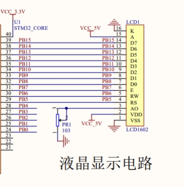
LCD display is divided into field display and character display. The field display is similar to the LED display, which can be displayed as long as the corresponding signal is sent to the corresponding pin. Character display is to display basic characters as needed. This design adopts character display. In the system, LCD1602 is used as the display device to output information. Compared with the traditional LED digital tube display device, the liquid crystal display module has the advantages of small volume, low power consumption and rich display content, and does not need additional driving circuit. Now the liquid crystal display module is the most commonly used display device in the application design of single chip microcomputer. LCD1602 can display 2 lines of 16 Chinese characters.
2.5. 2. Circuit design of ADXL345 inclination sensor module
This design selects ADXL345 module of inclination sensor to detect relevant state information in real time. ADXL345 is a small and thin ultra-low power 3-axis accelerometer with high resolution (13 bits) and a measurement range of ± 16g. The digital output data is in 16 bit binary complement format and can be accessed through SPI(3-wire or 4-wire) or I2C digital interface. ADXL345 is ideal for mobile device applications. It can measure static gravity acceleration in tilt detection applications, as well as dynamic acceleration caused by motion or impact. Its high resolution (3.9mg/LSB) can measure tilt angle changes of less than 1.0 °. The device provides a variety of special detection functions. The active and inactive detection functions detect the occurrence of motion by comparing the acceleration on any axis with the threshold set by the user. The knock detection function can detect single vibration and double vibration in any direction. The free fall detection function can detect whether the device is falling. These functions can be independently mapped to one of the two interrupt output pins. The patent pending integrated memory management system adopts a 32 level first in first out (FIFO) buffer, which can be used to store data, so as to minimize the host processor load and reduce the overall system power consumption. Low power mode supports motion based intelligent power management, so as to carry out threshold sensing and motion acceleration measurement with very low power consumption.
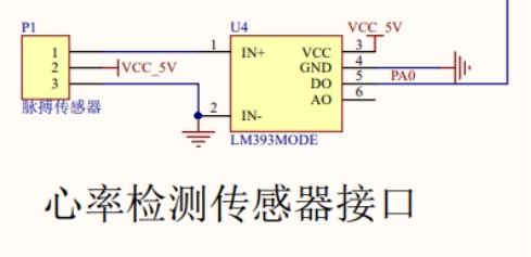
2.5. 3. Circuit design of Pulsesensor pulse and heart rate sensor module
Pulse heart rate sensor is a sensor used to test heart rate. In essence, it is an optical heart rate sensor integrating amplification circuit and noise elimination circuit. This sensor can be used to develop interactive works related to heart rate. Sensors can be worn on fingers or earlobes. The photoelectric sensor converts the pulse signal into an electrical signal. The device needs to place the finger on the sensor dial. The photoelectric sensor is an optical heart rate sensor integrating an amplification circuit and a noise elimination circuit. The light-emitting diode on one side of the photoelectric sensor emits light. When the pulse beats, the arterial blood volume of the fingertip or earlobe changes periodically, The light intensity through the fingertips changes simultaneously. The photoelectric triode on the other side converts the received infrared light signal into an electrical signal.
2.5. 4. Circuit design of DS18B20 temperature sensor module
DS18B20 is a commonly used digital temperature sensor. Its output is digital signal. It has the characteristics of small volume, low hardware overhead, strong anti-interference ability and high precision. DS18B20 digital temperature sensor has convenient wiring and can be applied to a variety of occasions after packaging, such as pipeline type, threaded type, magnet adsorption type, stainless steel packaging type. There are a variety of models, including LTM8877, LTM8874 and so on. The appearance is mainly changed according to different applications. The packaged DS18B20 can be used for various non limit temperature occasions, such as cable trench temperature measurement, blast furnace water circulation temperature measurement, boiler temperature measurement, machine room temperature measurement, agricultural greenhouse temperature measurement, clean room temperature measurement, ammunition depot temperature measurement and so on. The utility model has the advantages of wear resistance, collision resistance, small volume, convenient use and various packaging forms, and is suitable for the field of digital temperature measurement and control of various narrow space equipment.
3. STM32 performance introduction and hardware design
3.1 performance introduction of STM32 single chip microcomputer
STM32 has resources including 48KB SRAM, 256KB FLASH, 2 basic timers, 4 general timers, 2 advanced timers, 2 DMA controllers (12 channels in total), 3 SPI s, 2 IIC S, 5 serial ports, 1 USB, 1 CAN, 3 12 bit ADC s, 1 12 bit DAC, 1 SDIO interface and 51 general IO ports. The chip has high cost performance.
The description of each pin is as follows:
-
PA0 function 1, press KEY_UP 2 can be used as standby wake-up pin (WKUP) 3, and can be connected to DS18B20 sensor interface (P2 setting)
-
PA1 function 1, NRF24L01 interface IRQ signal 2, connected to HS0038 infrared receiver (P2 setting)
-
PA2 acts as the chip selection signal of W25Q64
-
PA3 acts as the chip selection pin of SD card interface
-
PA4 acts as CE signal of NRF24L01 interface
-
PA5 acts as SCK signal of W25Q64, SD card and NRF24L01 interface
-
PA6 acts as MISO signal of W25Q64, SD card and NRF24L01 interface
-
PA7 acts as MOSI signal of W25Q64, SD card and NRF24L01 interface
-
PA8 is used to connect DS0 LED lamp (red)
-
PA9 acts as TX pin of serial port 1, and is connected to RX of CH340 by default (P4 setting)
-
PA10 acts as RX pin of serial port 1, and is connected to TX(P4 setting) of CH340 by default
-
PA11 acts as a USB D-pin
-
PA12 acts as a USB D + pin
-
PA13 acts as JTAG/SWD simulation interface without any peripherals
-
PA14 acts as JTAG/SWD simulation interface without any peripherals
-
PA15 acts as 1, JTAG simulation port (JTDI) 2, CLK signal 3 of PS/2 interface, and connected to key 1
3.2 hardware design of intelligent Bracelet system
The main circuit diagram, temperature detection module circuit diagram, step counting module circuit diagram, heart rate sensor module circuit diagram and LCD external wiring diagram required by the program are shown in the following figure in turn:


4. System program
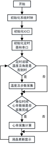
4.1 main program design flow chart
4.2 main program content
#include "led.h"
#include "delay.h"
#include "sys.h"
#include "usart.h"
#include <stdio.h>
#include "timer.h"
#include "key.h"
#include "exti.h"
#include "adxl345.h"
#include "lcd1602.h"
#include "ds18b20.h"

unsigned char ReadAdxl345;	   //Read adxl345 data regularly
unsigned char ErrorNum=0;   //Record the number of errors
unsigned char CheckNum=0;   //Detection times

char dis0[16];//LCD array display temporary storage
char dis1[35];

unsigned int xlTab[5];//Heart rate array
unsigned char count=0;	//Heart rate filter count
unsigned int xinLater=0;//	Heart rate delay processing
unsigned int xinLv =0;    //Heart rate value

unsigned int BuShu=0;//Number of steps
unsigned int Normal_num=0;			//Normal times
unsigned int Error_num=0;			//Tilt times

unsigned int disBuShu = 0;  //Show steps
float disJuLi = 0;//Display distance
float temperature;  //temperature
unsigned char readTemp = 0;	//Read temperature flag

int main(void)
{
    delay_init();	    	 //Delay function initialization
    uart_init(9600);	 	//The serial port is initialized to 9600
    TIM3_Int_Init(49,7199);//50ms
    EXTIX_Init();		// Initialize external interrupt
    LED_Init();		  		//Initialize the hardware interface to the LED
    KEY_Init();			//Initialization key
    Lcd_GPIO_init();  //Initialize lcd pin
    Lcd_Init();		  //Initialize lcd screen
    delay_ms(200);

    Init_ADXL345();
    if(Single_Read_ADXL345(0X00)==0xe5)
    {
        delay_ms(5);
    }
    else
    {
        delay_ms(3);
    }
    while(1)
    {
        if(ReadAdxl345== 1)   //Read adxl345 data regularly
        {
            ReadAdxl345= 0;
            ReadData_x();  						//Triaxial detection function
            CheckNum++;
            if((temp_Y>450)||(temp_Y<-450)) //View normal times
            {
                Normal_num++;  //Normal times++
            }
            else
            {
                Error_num++;//Tilt times
            }
            if((Error_num!=0)&&(Normal_num!=0))//Steps detected
            {
                BuShu++;   //Step pulse++
                Error_num=0;    //Clear one cycle detection
                Normal_num=0;
            }
        }
        if(disFlag==1)	   //Display flag
        {
            disFlag = 0;
            readTemp++;  //Timing count
            if(readTemp >= 8)//Primary data processing temperature of about 800ms
            {
                readTemp =0;//Re count
                temperature=(float)DS18B20_Get_Temp()/10;	//Reduce 10 times to actual value
            }
            disBuShu = BuShu/2;  //Show steps
            disJuLi = disBuShu*0.45;//Display distance
            sprintf(dis0,"X:%03d/min %4.1f C",xinLv,temperature);//Print
            Lcd_Puts(0,0,(unsigned char *)dis0);	//display
            Lcd_1Put(14,0,0xdf);//display symbols
            sprintf(dis1,"BS:%03d JL:%4.1fm  ",disBuShu,disJuLi);//Print
            Lcd_Puts(0,1,(unsigned char *)dis1);	//display

        }
    }
}
4.3 ADXL345 inclination sensor
#include "stm32f10x.h"
#include "delay.h"
#include "adxl345.h"

#define SDA_RCC			RCC_APB2Periph_GPIOA
#define SDA_GPIO		GPIOA
#define SDA_GPIO_PIN	GPIO_Pin_5

#define SCL_RCC			RCC_APB2Periph_GPIOA
#define SCL_GPIO		GPIOA
#define SCL_GPIO_PIN	GPIO_Pin_4

#define SCL_OUT() SCL_Set_Output() / / set scl
#define SET_SCL() GPIO_SetBits(SCL_GPIO, SCL_GPIO_PIN) / / set SCL
#define CLE_SCL() GPIO_ResetBits(SCL_GPIO, SCL_GPIO_PIN) / / clear SCL

#define SDA_OUT() SDA_Set_Output()
#define SDA_INT() SDA_Set_Input()
#define SET_SDA() GPIO_SetBits(SDA_GPIO, SDA_GPIO_PIN) / / set SDA
#define CLE_SDA() GPIO_ResetBits(SDA_GPIO, SDA_GPIO_PIN) / / clear SDA
#define SDA_VAL() GPIO_ReadInputDataBit(SDA_GPIO, SDA_GPIO_PIN)

#define 	 Slaveaddress 0xA6 / / defines the slave address of the device in the IIC bus. It is modified according to the ALT address pin / / the address of the ALT address pin is 0xA6 when it is grounded and 0x3A when it is connected to the power supply

unsigned char BUF[8];                         //Receive data buffer
unsigned char ge,shi,bai,qian,wan;           //Display variables
unsigned char err;
float temp_X,temp_Y,temp_Z;

void SCL_Set_Output(void)
{
	GPIO_InitTypeDef  GPIO_InitStructure;
	GPIO_InitStructure.GPIO_Pin = SCL_GPIO_PIN;
	GPIO_InitStructure.GPIO_Mode = GPIO_Mode_Out_PP;
	GPIO_InitStructure.GPIO_Speed = GPIO_Speed_50MHz;
	GPIO_Init(SCL_GPIO, &GPIO_InitStructure);
}

void SDA_Set_Output(void)
{
	GPIO_InitTypeDef  GPIO_InitStructure;
	GPIO_InitStructure.GPIO_Pin = SDA_GPIO_PIN;
	GPIO_InitStructure.GPIO_Mode = GPIO_Mode_Out_PP;
	GPIO_InitStructure.GPIO_Speed = GPIO_Speed_50MHz;
	GPIO_Init(SDA_GPIO, &GPIO_InitStructure);
}

void SDA_Set_Input(void)
{
	GPIO_InitTypeDef  GPIO_InitStructure;
	GPIO_InitStructure.GPIO_Pin = SDA_GPIO_PIN;
	GPIO_InitStructure.GPIO_Mode = GPIO_Mode_IPU;
	GPIO_InitStructure.GPIO_Speed = GPIO_Speed_50MHz;
	GPIO_Init(SDA_GPIO, &GPIO_InitStructure);
}

/**************************************
Start signal
**************************************/
void ADXL345_Start(void)
{
    SCL_OUT();
    SDA_OUT();
    SET_SDA();//SDA = 1;                    // Pull up the data cable
    SET_SCL();//SCL = 1;                    // Pull up the clock line
    delay_us(2);//Delay5us();                 // delayed
    CLE_SDA();//SDA = 0;                    // Produce falling edge
    delay_us(2);//Delay5us();                 // delayed
    CLE_SCL();//SCL = 0;                    // Pull down the clock line
}

/**************************************
Stop signal
**************************************/
void ADXL345_Stop(void)
{
    SCL_OUT();
    SDA_OUT();
    CLE_SDA();//SDA = 0;                    // Pull down the data cable
    SET_SCL();//SCL = 1;                    // Pull up the clock line
    delay_us(2);//Delay5us();                 // delayed
    SET_SDA();//SDA = 1;                    // Produce rising edge
    delay_us(2);//Delay5us();                 // delayed
    CLE_SCL();
}

/**************************************
Send response signal
 Entry parameter: ack (0:ACK 1:NAK)
**************************************/
void ADXL345_SendACK(uchar ack)
{
    SCL_OUT();
    SDA_OUT();
    if(ack==0)//SDA = ack;                  // Write reply signal
    {
      CLE_SDA();
    }
    else
    {
      SET_SDA();
    }
    SET_SCL();//SCL = 1;                    // Pull up the clock line
    delay_us(2);//Delay5us();                 // delayed
    CLE_SCL();//SCL = 0;                    // Pull down the clock line
    delay_us(5);//Delay5us();                 // delayed
}
/**************************************
Receive response signal
**************************************/
uchar ADXL345_RecvACK(void)
{
    SDA_INT();
    SCL_OUT();
    SET_SCL();//SCL = 1;                    // Pull up the clock line
    delay_us(2);//    Delay5us();                 // delayed
    SET_SCL();
    if(SDA_VAL()== Bit_SET)   //CY = SDA;                   // Read response signal
    {
        err = 1;
    }
    else
    {
        err = 0;
    }
    CLE_SCL() ;//SCL = 0;                    // Pull down the clock line
    delay_us(5);//    Delay5us();                 // delayed
    SDA_OUT();
    return err;
}

/**************************************
Sends a byte of data to the IIC bus
**************************************/
void ADXL345_SendByte(unsigned char dat)
{
    unsigned char i;
    SCL_OUT();
    SDA_OUT();
    for (i=0; i<8; i++)         //8-bit counter
    {
        delay_us(5);             //delayed
        if(dat&0x80)  //SDA = CY;               // Data transmission port
        {SET_SDA();}
        else
        {CLE_SDA();}
        delay_us(5);             //delayed
        SET_SCL();//SCL = 1;                // Pull up the clock line
        delay_us(5);             //delayed
        CLE_SCL();//SCL = 0;                // Pull down the clock line
        dat <<= 1;              //Remove the highest bit of data
    }
    ADXL345_RecvACK();
}
/**************************************
Receives a byte of data from the IIC bus
**************************************/
unsigned char ADXL345_RecvByte(void)
{
    unsigned char i;
    unsigned char Mid;
    unsigned char dat = 0;
    SDA_INT();
    SCL_OUT();

    for (i=0; i<8; i++)         //8-bit counter
    {
        dat <<= 1;
        delay_us(5);            //delayed
        SET_SCL();

        if(SDA_VAL()== Bit_SET)   //CY = SDA;                   // Read response signal
        {
            Mid = 1;
        }
        else
        {
            Mid = 0;
        }
        if(Mid) dat++;
        delay_us(5);
        CLE_SCL();//SCL = 0;                // Pull down the clock line
    }
    return dat;
}

//******Single byte write*******************************************

void Single_Write_ADXL345(uchar REG_Address,uchar REG_data)
{
    ADXL345_Start();                  //Start signal
    ADXL345_SendByte(SlaveAddress);   //Sending device address + write signal
    ADXL345_SendByte(REG_Address);    //Internal register address
    ADXL345_SendByte(REG_data);       //Internal register data
    ADXL345_Stop();                   //Send stop signal
}

//********Single byte read*****************************************
uchar Single_Read_ADXL345(uchar REG_Address)
{
    uchar REG_data;
    ADXL345_Start();                          //Start signal
    ADXL345_SendByte(SlaveAddress);           //Sending device address + write signal
    ADXL345_SendByte(REG_Address);            //Send storage unit address, starting from 0
    ADXL345_Start();                          //Start signal
    ADXL345_SendByte(SlaveAddress+1);         //Sending device address + read signal
    REG_data=ADXL345_RecvByte();              //Read register data
    ADXL345_SendACK(1);
    ADXL345_Stop();                           //Stop signal
    return REG_data;
}
//Continuously read ADXL345 internal acceleration data, address range 0x32~0x37
void Multiple_Read_ADXL345(void)
{
    uchar i;
    ADXL345_Start();                          //Start signal
    ADXL345_SendByte(SlaveAddress);           //Sending device address + write signal
    ADXL345_SendByte(0x32);                   //Send storage unit address, starting from 0x32
    ADXL345_Start();                          //Start signal
    ADXL345_SendByte(SlaveAddress+1);         //Sending device address + read signal
    for (i=0; i<6; i++)                      //Continuously read 6 address data and store BUF in
    {
        BUF[i] = ADXL345_RecvByte();          //BUF[0] stores data in 0x32 address
        if (i == 5)
        {
            ADXL345_SendACK(1);                //The last data needs to be returned to NOACK
        }
        else
        {
            ADXL345_SendACK(0);                //Respond to ACK
        }
    }
    ADXL345_Stop();                          //Stop signal
    delay_ms(5);
}
//Initialize ADXL345
void Init_ADXL345(void)
{
    Single_Write_ADXL345(0x31,0x0B);   //Measurement range, plus or minus 16g, 13 bit mode
    Single_Write_ADXL345(0x2C,0x08);   //The rate is set to 12.5
    Single_Write_ADXL345(0x2D,0x08);   //Select power mode
    Single_Write_ADXL345(0x2E,0x80);   //Enable DATA_READY interrupt
    Single_Write_ADXL345(0x1E,0x00);   //The X offset is written according to the status of the test sensor
    Single_Write_ADXL345(0x1F,0x00);   //The Y offset is written according to the status of the test sensor
    Single_Write_ADXL345(0x20,0x05);   //The Z offset is written according to the status of the test sensor
}
//Show x axis
void ReadData_x(void)
{
    int  dis_data;                       //variable
    Multiple_Read_ADXL345();       	//Data is read out continuously and stored in BUF
    dis_data=(BUF[1]<<8)+BUF[0];  //Synthetic data
    temp_X=(float)dis_data*3.9;  //Calculation data and display
    dis_data=(BUF[3]<<8)+BUF[2];  //Synthetic data
    temp_Y=(float)dis_data*3.9;  //Calculation data and display
    dis_data=(BUF[5]<<8)+BUF[4];    //Synthetic data
    temp_Z=(float)dis_data*3.9;  //Calculation data and display
}
4.4 LCD1602 display screen
#include "lcd1602.h"

/************************Port initialization*******************************/
void Lcd_GPIO_init(void)
{
     GPIO_InitTypeDef GPIO_InitStructure;   //Declaration structure

    /********Data Port settings*************/
	 RCC_APB2PeriphClockCmd(RCC_GPIO_DATA, ENABLE);  //Open port B clock
     GPIO_InitStructure.GPIO_Pin  = GPIO_DATA_0_PIN|GPIO_DATA_1_PIN|GPIO_DATA_2_PIN|GPIO_DATA_3_PIN|GPIO_DATA_4_PIN|GPIO_DATA_5_PIN|GPIO_DATA_6_PIN|GPIO_DATA_7_PIN; //  DB8~DB15
     GPIO_InitStructure.GPIO_Mode = GPIO_Mode_Out_PP;  //Standard output mode
     GPIO_InitStructure.GPIO_Speed = GPIO_Speed_50MHz; //50M clock speed
     GPIO_Init(GPIO_DATA_0, &GPIO_InitStructure);      //Initialize port

	 /********Enable port settings**********/
	 RCC_APB2PeriphClockCmd(RCC_GPIO_EN, ENABLE);    	//Open port clock
     GPIO_InitStructure.GPIO_Pin =  GPIO_EN_PIN;     	// Enable port
     GPIO_InitStructure.GPIO_Mode = GPIO_Mode_Out_PP;  //Standard output mode
     GPIO_InitStructure.GPIO_Speed = GPIO_Speed_50MHz; //50M clock speed
     GPIO_Init(GPIO_EN, &GPIO_InitStructure);

	 /********Read / write port settings**********/
	 RCC_APB2PeriphClockCmd(RCC_GPIO_RW, ENABLE);    //Open port clock
     GPIO_InitStructure.GPIO_Pin =  GPIO_RW_PIN;     // Enable port
     GPIO_InitStructure.GPIO_Mode = GPIO_Mode_Out_PP;  //Standard output mode
     GPIO_InitStructure.GPIO_Speed = GPIO_Speed_50MHz; //50M clock speed
     GPIO_Init(GPIO_RW, &GPIO_InitStructure);

	 /********Command / data port settings**********/
	 RCC_APB2PeriphClockCmd(RCC_GPIO_RS, ENABLE);    //Open port clock
     GPIO_InitStructure.GPIO_Pin =  GPIO_RS_PIN;     // Enable port
     GPIO_InitStructure.GPIO_Mode = GPIO_Mode_Out_PP; //Push pull multiplex output
     GPIO_InitStructure.GPIO_Speed = GPIO_Speed_50MHz; //50M clock speed
     GPIO_Init(GPIO_RS, &GPIO_InitStructure);


}
/******************************************************************/


void Lcd_Init( void )  //initialization
{
    Lcd_GPIO_init();
    delay_us(1500);                     //Delay 15ms
    Lcd_Write_Command( 0x38,0);       // The write instruction 38H does not detect the busy signal
    delay_us(500);				      //Delay 5ms
    Lcd_Write_Command( 0x38,0);       // The write instruction 38H does not detect the busy signal
    delay_us(500);					  //Delay 5ms
    Lcd_Write_Command( 0x38,0);       // The write instruction 38H does not detect the busy signal
    //After that, the busy signal shall be detected before each write instruction and read / write data operation
    Lcd_Write_Command( 0x38,1);       //Display mode settings
    Lcd_Write_Command( 0x08,1);		  //Display off
    Lcd_Write_Command( 0x01,1);       //Display clear screen
    Lcd_Write_Command( 0x06,1);       //Display cursor movement settings
    Lcd_Write_Command( 0x0C,1); 	  //Display on, cursor not displayed
}
/******************************************************/

void Lcd_En_Toggle(void) //Enable pulse
{
	SET_EN;        //Enable 1
	delay_us(5);   //Delay 160us
	CLE_EN;
}


void Lcd_Busy(void)//Judgment busy
{
    unsigned int later0=0;
    GPIO_InitTypeDef GPIO_InitStructure;
    RCC_APB2PeriphClockCmd(RCC_GPIO_DATA, ENABLE);    //Open DATA port clock

    GPIO_InitStructure.GPIO_Pin  = 	GPIO_DATA_0_PIN|GPIO_DATA_1_PIN|GPIO_DATA_2_PIN|GPIO_DATA_3_PIN|GPIO_DATA_4_PIN|GPIO_DATA_5_PIN|GPIO_DATA_6_PIN|GPIO_DATA_7_PIN; //  DB8~DB15
    GPIO_InitStructure.GPIO_Mode = GPIO_Mode_IPU; //Input mode = pull up input
    GPIO_InitStructure.GPIO_Speed = GPIO_Speed_50MHz; //50M clock speed
    GPIO_Init(GPIO_DATA_7, &GPIO_InitStructure);      //Open busy detection port

    CLE_RS; //RS = 0
    //delay_us(1);   // Delay 10us
    SET_RW; //RW = 1
    //delay_us(1);   // Delay 10us
    SET_EN; //EN = 1
    //delay_us(2);   // Delay 20us
    while ((GPIO_ReadInputDataBit(GPIO_DATA_7,GPIO_DATA_7_PIN))&&(later0<20000)) //Circular waiting busy detection port = 0
    {
        delay_us(5);
        later0++;
    }
    CLE_EN; //EN = 0

    //Restore port to output state
    RCC_APB2PeriphClockCmd(RCC_GPIO_DATA, ENABLE);    //Open DATA port clock
    GPIO_InitStructure.GPIO_Pin  = GPIO_DATA_0_PIN|GPIO_DATA_1_PIN|GPIO_DATA_2_PIN|GPIO_DATA_3_PIN|GPIO_DATA_4_PIN|GPIO_DATA_5_PIN|GPIO_DATA_6_PIN|GPIO_DATA_7_PIN; //  DB8~DB15
    GPIO_InitStructure.GPIO_Mode = GPIO_Mode_Out_PP; //Push pull output
    GPIO_InitStructure.GPIO_Speed = GPIO_Speed_50MHz; //50M clock speed
    GPIO_Init(GPIO_DATA_7, &GPIO_InitStructure);

}

void Gpio_data(unsigned char x)  //Port placement data
{
    GPIO_ResetBits(GPIO_DATA_0, GPIO_DATA_0_PIN);  //DB0
    GPIO_ResetBits(GPIO_DATA_0, GPIO_DATA_1_PIN);  //DB1
    GPIO_ResetBits(GPIO_DATA_0, GPIO_DATA_2_PIN);  //DB2
    GPIO_ResetBits(GPIO_DATA_0, GPIO_DATA_3_PIN);  //DB3
    GPIO_ResetBits(GPIO_DATA_0, GPIO_DATA_4_PIN);  //DB4
    GPIO_ResetBits(GPIO_DATA_0, GPIO_DATA_5_PIN);  //DB5
    GPIO_ResetBits(GPIO_DATA_0, GPIO_DATA_6_PIN);  //DB6
    GPIO_ResetBits(GPIO_DATA_0, GPIO_DATA_7_PIN);  //DB7
    if(x&0X01)GPIO_SetBits(GPIO_DATA_0, GPIO_DATA_0_PIN);//DB0
    if(x&0X02)GPIO_SetBits(GPIO_DATA_0, GPIO_DATA_1_PIN);//DB1
    if(x&0X04)GPIO_SetBits(GPIO_DATA_0, GPIO_DATA_2_PIN);//DB2
    if(x&0X08)GPIO_SetBits(GPIO_DATA_0, GPIO_DATA_3_PIN);//DB3
    if(x&0X10)GPIO_SetBits(GPIO_DATA_0, GPIO_DATA_4_PIN);//DB4
    if(x&0X20)GPIO_SetBits(GPIO_DATA_0, GPIO_DATA_5_PIN);//DB5
    if(x&0X40)GPIO_SetBits(GPIO_DATA_0, GPIO_DATA_6_PIN);//DB6
    if(x&0X80)GPIO_SetBits(GPIO_DATA_0, GPIO_DATA_7_PIN);//DB7
}

//Write instruction sequence to LCD: RS=L,RW=L,Data0-Data7 = instruction code, E = high pulse
void Lcd_Write_Command(unsigned char x,char Busy)
{
    if(Busy) Lcd_Busy();
    //delay_us(1);   // Delay 10us
	CLE_RS;  //RS = 0
    //delay_us(1);   // Delay 10us
	CLE_RW;  //RW = 0
    //delay_us(4);   // Delay 40us
    Gpio_data(x);  //Port placement data
    //delay_us(4);   // Delay 40us
	Lcd_En_Toggle();  //Enable pulse
    //delay_us(1);   // Delay 100us
	Lcd_Busy(); //Busy measurement

}
//Time sequence for writing data into LCD: RS=H,RW=L,Data0-Data7 = instruction code, E = high pulse
void Lcd_Write_Data( unsigned char x) //Write data to the LCD
{
	Lcd_Busy(); //Busy measurement
    //delay_us(1);   // Delay 10us
	SET_RS;   //RS = 1
    //delay_us(1);   // Delay 10us
    CLE_RW;   //RW = 0
    //delay_us(4);   // Delay 40us
    Gpio_data(x);
    //delay_us(4);   // Delay 40us
	Lcd_En_Toggle();  //Enable pulse
    //delay_us(1);   // Delay 100us
	Lcd_Busy(); //Busy measurement

}
void Lcd_SetXY(unsigned char x,unsigned char y)   //Character initial position setting, x represents column and y represents row
{
    unsigned char addr;
    if(y==0)
        addr=0x80+x;
    else if(y==1)
        addr=0xC0+x;
    Lcd_Write_Command(addr,1) ;
}
void Lcd_Puts(unsigned char x,unsigned char y, unsigned char *string) //Write a string to 1602
{
    Lcd_SetXY(x,y);
    while(*string)
    {
        Lcd_Write_Data(*string);
        string++;
    }
}
void Lcd_1Put(unsigned char x,unsigned char y, unsigned char Data0)
{
   	Lcd_SetXY(x,y);
	Lcd_Write_Data(Data0);
}
4.5. DS18B20 temperature sensor
#include "ds18b20.h"
#include "delay.h"

	//IO direction setting
//#define DS18B20_IO_IN()  {GPIOA->CRL&=0XFFFFFFF0;GPIOA->CRL|=8<<0;}
//#define DS18B20_IO_OUT() {GPIOA->CRL&=0XFFFFFFF0;GPIOA->CRL|=3<<0;}

void DS18B20_IO_IN(void)
{
	GPIO_InitTypeDef GPIO_InitStructure;

 	RCC_APB2PeriphClockCmd(RCC_GPIO_DQ,ENABLE);//Enable PORTA,PORTC clock

	GPIO_InitStructure.GPIO_Pin  = GPIO_DQ_PIN;
	GPIO_InitStructure.GPIO_Mode = GPIO_Mode_IPU; //Set as pull-up input
 	GPIO_Init(GPIO_DQ, &GPIO_InitStructure);//initialization
}

void DS18B20_IO_OUT(void)
{
 GPIO_InitTypeDef  GPIO_InitStructure;

 RCC_APB2PeriphClockCmd(RCC_GPIO_DQ, ENABLE);	 //Enable

 GPIO_InitStructure.GPIO_Pin = GPIO_DQ_PIN;
 GPIO_InitStructure.GPIO_Mode = GPIO_Mode_Out_PP; 		 //Push pull output
 GPIO_InitStructure.GPIO_Speed = GPIO_Speed_50MHz;		 //The speed of IO port is 50MHz
 GPIO_Init(GPIO_DQ, &GPIO_InitStructure);					 //Initialize according to the set parameters
}
//Initialize the IO port DQ of DS18B20 and detect the existence of DS at the same time
//Return 1: does not exist
//Return 0: exists
u8 DS18B20_Init(void)
{
 	GPIO_InitTypeDef  GPIO_InitStructure;

 	RCC_APB2PeriphClockCmd(RCC_GPIO_DQ, ENABLE);	 //Enable PORTA port clock

 	GPIO_InitStructure.GPIO_Pin = GPIO_DQ_PIN;				//PORTA0 push pull output
 	GPIO_InitStructure.GPIO_Mode = GPIO_Mode_Out_PP;
 	GPIO_InitStructure.GPIO_Speed = GPIO_Speed_50MHz;
 	GPIO_Init(GPIO_DQ, &GPIO_InitStructure);

 	GPIO_SetBits(GPIO_DQ,GPIO_DQ_PIN);    //Output 1

	DS18B20_Rst();

	return DS18B20_Check();
}


//Reset DS18B20
void DS18B20_Rst(void)
{
	DS18B20_IO_OUT(); //SET PA0 OUTPUT
    DS18B20_DQ_OUT=0; //Pull down DQ
    delay_us(750);    //Pull down 750us
    DS18B20_DQ_OUT=1; //DQ=1
	delay_us(15);     //15US
}
//Waiting for a response from DS18B20
//Return 1: the existence of DS18B20 is not detected
//Return 0: exists
u8 DS18B20_Check(void)
{
	u8 retry=0;
	DS18B20_IO_IN();//SET PA0 INPUT
    while (DS18B20_DQ_IN&&retry<200)
	{
		retry++;
		delay_us(1);
	};
	if(retry>=200)return 1;
	else retry=0;
    while (!DS18B20_DQ_IN&&retry<240)
	{
		retry++;
		delay_us(1);
	};
	if(retry>=240)return 1;
	return 0;
}
//Read a bit from DS18B20
//Return value: 1 / 0
u8 DS18B20_Read_Bit(void) 			 // read one bit
{
    u8 data;
	DS18B20_IO_OUT();//SET PA0 OUTPUT
    DS18B20_DQ_OUT=0;
	delay_us(2);
    DS18B20_DQ_OUT=1;
	DS18B20_IO_IN();//SET PA0 INPUT
	delay_us(12);
	if(DS18B20_DQ_IN)data=1;
    else data=0;
    delay_us(50);
    return data;
}
//Read a byte from DS18B20
//Return value: read data
u8 DS18B20_Read_Byte(void)    // read one byte
{
    u8 i,j,dat;
    dat=0;
	for (i=1;i<=8;i++)
	{
        j=DS18B20_Read_Bit();
        dat=(j<<7)|(dat>>1);
    }
    return dat;
}
//Write a byte to DS18B20
//dat: bytes to write
void DS18B20_Write_Byte(u8 dat)
 {
    u8 j;
    u8 testb;
	DS18B20_IO_OUT();//SET PA0 OUTPUT;
    for (j=1;j<=8;j++)
	{
        testb=dat&0x01;
        dat=dat>>1;
        if (testb)
        {
            DS18B20_DQ_OUT=0;// Write 1
            delay_us(2);
            DS18B20_DQ_OUT=1;
            delay_us(60);
        }
        else
        {
            DS18B20_DQ_OUT=0;// Write 0
            delay_us(60);
            DS18B20_DQ_OUT=1;
            delay_us(2);
        }
    }
}
//Start temperature conversion
void DS18B20_Start(void)// ds1820 start convert
{
    DS18B20_Rst();
	DS18B20_Check();
    DS18B20_Write_Byte(0xcc);// skip rom
    DS18B20_Write_Byte(0x44);// convert
}

//Get the temperature value from ds18b20
//Accuracy: 0.1C
//Return value: temperature value (- 550 ~ 1250)
short DS18B20_Get_Temp(void)
{
    u8 temp;
    u8 TL,TH;
	short tem;
    DS18B20_Start ();                    // ds1820 start convert
    DS18B20_Rst();
    DS18B20_Check();
    DS18B20_Write_Byte(0xcc);// skip rom
    DS18B20_Write_Byte(0xbe);// convert
    TL=DS18B20_Read_Byte(); // LSB
    TH=DS18B20_Read_Byte(); // MSB

    if(TH>7)
    {
        TH=~TH;
        TL=~TL;
        temp=0;//The temperature is negative
    }else temp=1;//The temperature is positive
    tem=TH; //Get the top eight
    tem<<=8;
    tem+=TL;//Get the bottom eight
    tem=(float)tem*0.625;//transformation
	if(temp)return tem; //Return temperature value
	else return -tem;
}
5. System debugging and analysis
5.1 system commissioning
Before the power on commissioning of the overall system, observe that there are still problems in the welded system, such as obvious fracture, reverse connection of positive and negative electrodes, connection, false welding, etc., and then use a multimeter to detect whether there are serious power supply problems such as short circuit between the positive and negative electrodes of the power supply, so as to finally ensure that there is no problem in the welding of the system. After setting up the debugging platform, the software program needs to be debugged. If there is no problem with the program debugging, then start to verify whether the system function meets the requirements. If there is a problem with the function, continue to debug the program and repeat it until all functions are met.
5.2 commissioning phenomenon and analysis
After entering the debugging state, breakpoints should be set at key places, and then run step by step. At the same time, observe the changes of parameters, judge the process of program operation through changes, and then find out the chaotic parts in the program and correct them. This requires a good grasp of the software and a good understanding of the language program. After the experimental board is built successfully, We entered the stage of program design and debugging. We started to write the program smoothly, but later there were many errors in the debugging process, such as the setting of timer accuracy and the call of subroutines. The most difficult thing is the analysis of the execution sequence of the program without steps. Due to the wrong understanding of some statements in the program and the wrong judgment of the execution sequence, Let me fall into a misunderstanding and delay for a long time. Finally, with the help of my classmates, I finally found the wrong key point and corrected it successfully. It seems that I still need to strengthen the debugging ability of the program. The debugging of the program requires patience and proficiency in some functions of the software.
5.3 test results
The system functions normally and can realize the contents specified in the design requirements and purposes. The following is the result diagram:
