Full tutorial download address: http://www.armbbs.cn/forum.php?mod=viewthread&tid=86980
Chapter 93 driving ADS1256 for SPI bus application of STM32H7 (8-channel 24bit ADC, gain programmable)
This chapter explains the implementation of 8-channel 24bit ADC chip driver.
93.1 important tips for beginners
93.2 ADC structure classification
93.3 ADS1256 hardware design
93.4 arrangement of key knowledge points of ADS1256 (important)
93.5 ADS1256 drive design
93.6 ADS1256 board level support package (bsp_spi_ads1256)
93.7 actual test effect of ADS1256 (10uV jitter)
93.8 ADS1256 driver transplantation and use
93.9 experimental routine design framework
93.10 experimental routine description (MDK)
93.11 experimental routine description (IAR)
93.12 summary
93.1 important tips for beginners
- The analog part of ADS1256 is powered by 5V, and the SPI digital interface level is 3.3V.
- PGA programmable gain support of ADS1256: 1, 2, 4, 8, 16, 32 and 64.
- ADS1256 supports automatic calibration (self calibration will be started when PGA,BUF enable and data sampling rate are set).
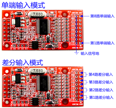
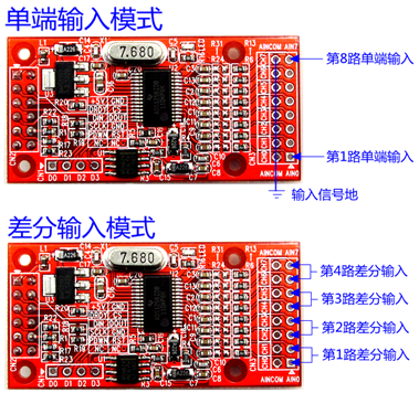
- ADS1256 supports 8-channel single ended ADC acquisition or 4-channel differential acquisition.
- ADS1256 supports positive and negative 5V differential acquisition, but does not support negative pressure. Pay attention when using.
- ADS1256 timing operation is a little special, so this chapter adopts analog SPI control.
- ADS1256 data manual, module schematic diagram (general version) and wiring diagram have been placed in the Doc file of the tutorial configuration example in this chapter.
- ADC's technical term interpretation document is recommended for you to see: http://www.armbbs.cn/forum.php?mod=viewthread&tid=89414 .
- When testing, be sure to use an external power supply to power the development board, because ADS1256 requires 5V power supply voltage. Pay attention to alignment when inserting ADS1256 module into the board.
93.2 ADC structure classification
Here we will popularize the six DAC structures. Note, these knowledge are translated from the English technical manuals of Meixin and TI.
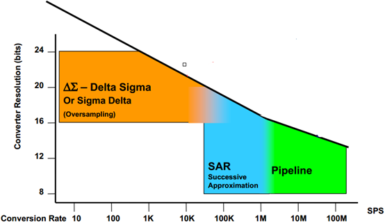
93.2.1 SAR ADC (successive approximation type)
Successive approximation ADC is usually the preferred architecture for medium and high resolution, and the sampling rate is usually lower than 5Msps. The most common resolution range of SAR ADC is 8-20 bits, and it has the characteristics of low power consumption and small size. This combination makes it very suitable for various applications, such as automatic test equipment, battery powered equipment, data acquisition system, medical instruments, motor and process control, and industry Automation, telecommunications, testing and measurement, portable systems, high-speed closed-loop systems and narrowband receivers.
93.2.2 Sigma-Delta ADC
Sigma delta ADC is mainly used in low-speed applications, which need to weigh speed and resolution through oversampling, and then filter to reduce noise. 24 bit sigma delta converter is used in automatic test equipment, high-precision portable sensors, medical and scientific instruments, seismic data acquisition and other applications.
93.2.3 Integrating ADC
Integrated ADC s provide high resolution and can provide good line frequency and noise suppression. The integrated architecture provides a novel and direct method to convert low bandwidth analog signals into digital representation. These types of converters usually include built-in drivers for LCD or LED displays and can be found in many portable instrument applications, including digital Panel meter and digital multimeter.
93.2.4 FLASH ADC
Flash ADC s are the fastest way to convert analog signals into digital signals. They are suitable for applications that require very large bandwidth. However, flash converters have high power, relatively low resolution, and can be very expensive. This limits them to high-frequency applications that cannot usually be solved in any other way. Examples include data acquisition, satellite communication, radar processing, Oscilloscope and high density disk drive.
93.2.5 Pipelined ADC
Pipelined ADCs have become the most popular ADC architecture, with sampling rates ranging from a few megabits per second (MS / s) to up to 100MS / s +, and resolutions of 8 to 16 bits. They provide resolution and sampling rates that can cover a variety of applications, including CCD imaging, ultrasonic medical imaging, digital receivers, base stations, and digital video (such as HDTV) , xDSL, cable modem and fast Ethernet.
93.2.6 Two Step ADC
Two step ADC is also called sub range converter, sometimes called multi-step or half flash (slower than Flash Architecture). This is the intersection of Flash ADC and pipelined ADC. Compared with Flash ADC, it can achieve higher resolution or smaller bare chip size.
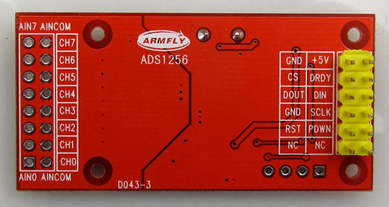
93.3 ADS1256 hardware design
Here, the ADS1256 hardware interface and ADS1256 module on the development board will be described for you.
ADS1256 schematic Forum Download:
http://www.armbbs.cn/forum.php?mod=viewthread&tid=97547 .
93.3.1 ADS1256 hardware interface
The schematic diagram of ADS1256 module socket on V7 board is as follows:
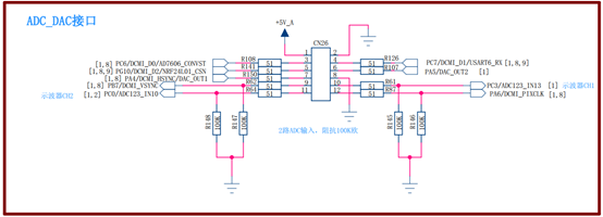
The actual location of the corresponding development board is as follows:

In order to facilitate better understanding of wiring, the following is the block diagram:
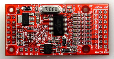
93.3.2 ADS1256 module
Product specification:
1. Single power supply 5.0V DC power supply, providing positive and negative 5V signal sampling function.
2. MCU interface: SPI.
3. Main ADC chip: ADS1256 (new imported original genuine).
4. Voltage reference, LM285-2.5 used before, and REF5025 (new imported original genuine product) used now.
5. The input circuit is equipped with voltage dividing resistor and R-C filter, which is convenient for customers to change the gain range.
6. Programmable gain amplifier in the chip, gain range: 1-64 times.
7. The internal input of the chip has a buffer amplifier, which can be directly connected to the sensor.
positive:
the other side:
Wiring diagram:
93.4 arrangement of key knowledge points of ADS1256 (important)
Driving ADS1256 requires an understanding of the following knowledge points.
93.4.1 ADS1256 basic information
ADS1256 is a micro power, high-precision, 8-Channel, 24 bit △ - ∑ high-performance analog-to-digital converter (ADC) launched by TI company. The device provides noise-free accuracy of up to 23 bits, data rate of up to 30kSPS (sub sampling / s), 0.0010% nonlinear characteristics (maximum) and many on-board peripherals (input analog multiplexer, input buffer, programmable gain amplifier and programmable digital filter, etc.) can bring complete and high-resolution measurement solutions to designers.
- 24 bit no data loss;
- Noise free accuracy up to 23 bits;
- Low nonlinearity: ± 0.0010%;
- The data sampling rate can reach 30kSPS;
- Single cycle conversion mode is adopted;
- With analog multi-channel switch and sensor interface (can be configured as 4-channel differential input or 8-channel monopole input);
- With input buffer (BUF);
- With serial peripheral interface (SPI);
- Low noise programmable gain amplifier (PGA) is included, and all PGAs have self calibration and system calibration;
- When PGA= 1, it can provide an effective resolution of up to 25.3 bits;
- When PGA = 64, it can provide an effective resolution of up to 22.5 bits;
- The analog input voltage is 5V and the digital voltage is 1.8~3.6V;
- The power consumption is as low as 38mW in normal mode and 0.4mW in standby mode.
93.4.2 functions of common pins of ADS1256
Packaging form of ADS1256:
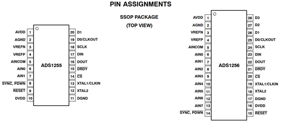
Here are some common pins:
- AVDD
Analog power supply.
- AGND
Simulated.
- VREFN
Negative reference voltage input.
- VREFP
Positive reference voltage input.
- AINCOM
Analog common input.
- AIN0 – AIN7
Analog input channel 0 to channel 7
- SYNC/PDWN
Synchronization, power down input.
- RESET
Reset pin.
- DVDD
Digital power supply.
- DGND
Digitally.
- XTAL1,XTAL2
Crystal oscillator input.
- CS
Chip selection input.
- DRDY
Data ready output signal pin.
- DOUT
Data output.
- DIN
Data entry.
- SCLK
Clock pin.
- D0,D1,D2,D3
General purpose GPIO
93.4.3 ADS1256 output voltage calculation formula
The calculation formula of ADS1256 is as follows:
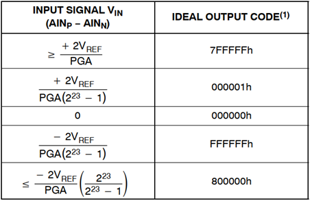
The minimum unit value is 2 * VREF/(PGA * (2^23 − 1))
It is represented by binary complement (in fact, it is a 24bit signed number. We can define the conversion result as int32_t).
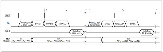
93.4.4 ADS1256 sequence diagram
The ADS1256 is driven mainly by two timing diagrams, which need to be understood, including read-write timing:
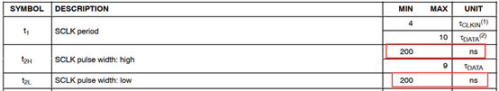
- t1: SPI clock cycle:
External crystal oscillator frequency = 7.68MHz,
Clock frequency tCLK = 1/7.68M = 0.13uS
Output data period Tdata = 1 / 30K = 0.033ms (calculated as 30Ksps)
Clock speed requirements for SPI:
The fastest 4 tCLK = 0.52uS
The slowest 10 tDATA = 0.3mS (calculated by 30Ksps)

- t2H, t2L: pulse high and low level:
The duration of SCL high level and low level shall be at least 200ns.

Data reading process:

- Step 1: ADS1256_ Setchannel (g_tads1256. Channel) switches the analog channel.
- Step 2: send SYNC synchronization command.
- Step 3: wake up.
- Step 4: read data.
In this process, pay special attention to reading the last converted data.
93.4.5 gain and measurement range of ADS1256
The relationship between the gain and measurement range of ADS1256 is as follows:
For example, when the gain is 1, the measurement range is plus or minus 5V, and when the gain is 64, the measurement range is plus or minus 78.125mV.
93.4.6 ADS1256 input buffer
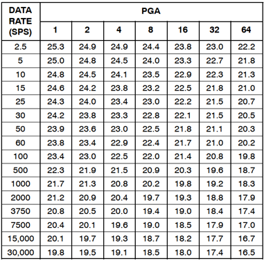
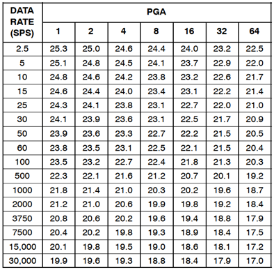
When switching the input buffer, we need to understand several parameters affected.
When buffering is on, input reference noise.
Input reference noise with buffer off:
With buffer on, effective resolution:
Number of significant digits when buffering is turned off:
Input impedance after opening the buffer:
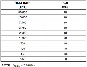
Input impedance after closing buffer:
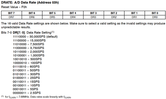
93.4.7 sampling rate supported by ADS1256
The sampling rates supported by ADS1256 are as follows. Pay special attention here because it takes 123 microseconds to switch channels and read data. Therefore, when scanning interrupt mode works, the maximum rate = DRATE_1000SPS.
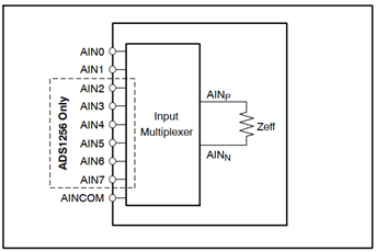
93.4.8 multiplexer for ADS1256, single ended and multi ended inputs
The 8-channel support of ADS1256 is realized through multiplexer. During 8-channel sampling, the corresponding channel is selected for sampling:
The practical effects of 8-channel single ended sampling and 4-channel differential sampling are as follows:
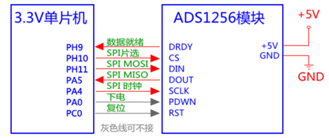
93.5 ADS1256 drive design
The program driver framework of ADS1256 is designed as follows:
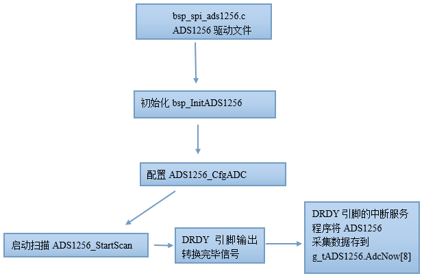
With this block diagram, the program design is easier to understand.
93.5.1 step 1, GPIO configuration involved in ADS1256
Here, you need to configure the GPIO clock and GPIO pin:
/*
    ADS1256 Module STM32-V7 development board (oscilloscope interface)
      +5V   <------  5.0V      5V power supply
      GND   -------  GND       land
      DRDY  ------>  PC6       Ready
      CS    <------  PC7       SPI_CS
      DIN   <------  PG10      SPI_MOSI
      DOUT  ------>  PA5       SPI_MISO
      SCLK  <------  PA4       SPI Clock
      GND   -------  GND       land
      PDWN  <------  PB7       Power down control
      RST   <------  PC3       Reset signal
      NC   Empty foot
      NC   Empty foot
*/

#ifdef SOFT_SPI / * software SPI*/
    /* Define GPIO ports */
    #define SCK_CLK_ENABLE()     __HAL_RCC_GPIOA_CLK_ENABLE()
    #define SCK_GPIO            GPIOA
    #define SCK_PIN            GPIO_PIN_4
    #define SCK_1()            SCK_GPIO->BSRR = SCK_PIN
    #define SCK_0()            SCK_GPIO->BSRR = ((uint32_t)SCK_PIN << 16U)

    #define DIN_CLK_ENABLE()     __HAL_RCC_GPIOG_CLK_ENABLE()
    #define DIN_GPIO            GPIOG
    #define DIN_PIN            GPIO_PIN_10
    #define DIN_1()            DIN_GPIO->BSRR = DIN_PIN
    #define DIN_0()            DIN_GPIO->BSRR = ((uint32_t)DIN_PIN << 16U)

    #define CS_CLK_ENABLE()     __HAL_RCC_GPIOC_CLK_ENABLE()
    #define CS_GPIO            GPIOC
    #define CS_PIN            GPIO_PIN_7
    #define CS_1()            CS_GPIO->BSRR = CS_PIN
    #define CS_0()            CS_GPIO->BSRR = ((uint32_t)CS_PIN << 16U)

    #define DOUT_CLK_ENABLE()     __HAL_RCC_GPIOA_CLK_ENABLE()
    #define DOUT_GPIO            GPIOA
    #define DOUT_PIN            GPIO_PIN_5
    #define DOUT_IS_HIGH()        ((DOUT_GPIO->IDR & DOUT_PIN) != 0)

    #define DRDY_CLK_ENABLE()     __HAL_RCC_GPIOC_CLK_ENABLE()
    #define DRDY_GPIO            GPIOC
    #define DRDY_PIN            GPIO_PIN_6
    #define DRDY_IS_LOW()        ((DRDY_GPIO->IDR & DRDY_PIN) == 0)
    #define DRDY_IRQn             EXTI9_5_IRQn
    #define DRDY_IRQHandler        EXTI9_5_IRQHandler

    /* PDWN  <------  PB7       Power down control */
    #define PWDN_CLK_ENABLE()     __HAL_RCC_GPIOB_CLK_ENABLE()
    #define PWDN_GPIO            GPIOB
    #define PWDN_PIN            GPIO_PIN_7
    #define PWDN_1()            PWDN_GPIO->BSRR = PWDN_PIN
    #define PWDN_0()            PWDN_GPIO->BSRR = ((uint32_t)PWDN_PIN << 16U)

    /*  RST   <------  PC3       Reset signal     */
    #define RST_CLK_ENABLE()     __HAL_RCC_GPIOC_CLK_ENABLE()
    #define RST_GPIO            GPIOC
    #define RST_PIN            GPIO_PIN_3
    #define RST_1()            RST_GPIO->BSRR = RST_PIN
    #define RST_0()            RST_GPIO->BSRR = ((uint32_t)RST_PIN << 16U)
#endif

/*
*********************************************************************************************************
*    Function name: bsp_InitADS1256
*    Function Description: configure the GPIO and SPI interfaces of STM32 to connect ADS1256
*    Formal parameters: None
*    Return value: None
*********************************************************************************************************
*/
void bsp_InitADS1256(void)
{
#ifdef SOFT_SPI
    GPIO_InitTypeDef gpio_init;

    RST_1();
    PWDN_1();
    CS_1();
    SCK_0();        /* SPI When the bus is idle, the clock line is low */
    DIN_1();

    /* Turn on GPIO clock */
    SCK_CLK_ENABLE();
    DIN_CLK_ENABLE();
    CS_CLK_ENABLE();
    DOUT_CLK_ENABLE();
    DRDY_CLK_ENABLE();
    PWDN_CLK_ENABLE();
    RST_CLK_ENABLE();

    /* Configure several push output IO */
    gpio_init.Mode = GPIO_MODE_OUTPUT_PP;        /* Set push-pull output */
    gpio_init.Pull = GPIO_NOPULL;                /* Pull up resistance not enabled */
    gpio_init.Speed = GPIO_SPEED_FREQ_HIGH;      /* GPIO Speed class */

    gpio_init.Pin = SCK_PIN;
    HAL_GPIO_Init(SCK_GPIO, &gpio_init);

    gpio_init.Pin = DIN_PIN;
    HAL_GPIO_Init(DIN_GPIO, &gpio_init);

    gpio_init.Pin = CS_PIN;
    HAL_GPIO_Init(CS_GPIO, &gpio_init);

    gpio_init.Pin = PWDN_PIN;
    HAL_GPIO_Init(PWDN_GPIO, &gpio_init);

    /* DRDY Set as input */
    gpio_init.Mode = GPIO_MODE_INPUT;        /* Set input */
    gpio_init.Pull = GPIO_NOPULL;            /* Pull up resistance not enabled */
    gpio_init.Speed = GPIO_SPEED_FREQ_HIGH;      /* GPIO Speed class */

    gpio_init.Pin = DRDY_PIN;
    HAL_GPIO_Init(DRDY_GPIO, &gpio_init);

    gpio_init.Pin = DOUT_PIN;
    HAL_GPIO_Init(DOUT_GPIO, &gpio_init);
#endif
}
Here, pay attention to the configuration of DRDY conversion ready pin, DRDY_IRQn and DRDY_IRQHandler should not be configured incorrectly.
93.5.2 step 2: implement the 8-bit read / write function of ADS1256
The read-write function is implemented as follows:
/*
*********************************************************************************************************
*    Function name: ADS1256_Send8Bit
*    Function Description: send 8 bit data to SPI bus. Without CS control.
*    Formal parameters:_ data: data
*    Return value: None
*********************************************************************************************************
*/
static void ADS1256_Send8Bit(uint8_t _data)
{
    uint8_t i;

    /* When multiple bytes are sent continuously, it needs to be delayed */
    ADS1256_DelaySCLK();
    ADS1256_DelaySCLK();

    /* ADS1256 SCL high and low level duration is required to be at least 200ns  */
    for(i = 0; i < 8; i++)
    {
        if (_data & 0x80)
        {
            DIN_1();
        }
        else
        {
            DIN_0();
        }
        SCK_1();
        ADS1256_DelaySCLK();
        _data <<= 1;
        SCK_0();            /* <----  ADS1256 Is to sample DIN data at the falling edge of SCK, and the data must be maintained at 50nS */
        ADS1256_DelaySCLK();
    }
}

/*
*********************************************************************************************************
*    Function name: ADS1256_Recive8Bit
*    Function Description: receive 8 bit data from SPI bus. Without CS control.
*    Formal parameters: None
*    Return value: None
*********************************************************************************************************
*/
static uint8_t ADS1256_Recive8Bit(void)
{
    uint8_t i;
    uint8_t read = 0;

    ADS1256_DelaySCLK();
    /* ADS1256 SCL high and low level duration is required to be at least 200ns  */
    for (i = 0; i < 8; i++)
    {
        SCK_1();
        ADS1256_DelaySCLK();
        read = read<<1;
        SCK_0();
        if (DOUT_IS_HIGH())
        {
            read++;
        }
        ADS1256_DelaySCLK();
    }
    return read;
}
Reading and writing are implemented in the following sequence:
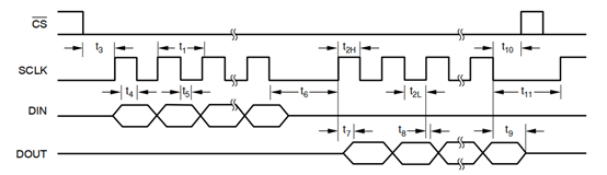
Here, we mainly pay attention to time realization:
t1: SPI clock cycle:
External crystal oscillator frequency = 7.68MHz,
Clock frequency tCLK = 1/7.68M = 0.13uS
Output data period Tdata = 1 / 30K = 0.033ms (calculated as 30Ksps)
Clock speed requirements for SPI:
The fastest 4 tCLK = 0.52uS
The slowest 10 tDATA = 0.3mS (calculated by 30Ksps)

t2H, t2L: pulse high and low level:
The duration of SCL high level and low level shall be at least 200ns.
93.5.3 step 3: read 24bit ADC data of ADS1256
The implementation code is as follows:
/*
*********************************************************************************************************
*    Function name: ADS1256_ReadData
*    Function Description: read ADC data
*    Formal parameters: None
*    Return value: None
*********************************************************************************************************
*/
static int32_t ADS1256_ReadData(void)
{
    uint32_t read = 0;

    CS_0();    /* SPI Film selection = 0 */

    ADS1256_Send8Bit(CMD_RDATA);    /* Command to read data */

    ADS1256_DelayDATA();    /* You must delay to read the data returned by the chip */

    /* Read the sampling result, 3 bytes, with the high byte first */
    read = ADS1256_Recive8Bit() << 16;
    read += ADS1256_Recive8Bit() << 8;
    read += ADS1256_Recive8Bit() << 0;

    CS_1();    /* SPI Film selection = 1 */

    /* Negative numbers are extended. 24 bit signed number extended to 32-bit signed number */
    if (read & 0x800000)
    {
        read += 0xFF000000;
    }

    return (int32_t)read;
}
The key in this code is the complement processing of 24bit data. Negative numbers are extended, and 24 bit signed numbers are extended to 32-bit signed numbers.
93.5.4 step 3, ADS1256 gain and sample rate configuration
The code is as follows:
/*
*********************************************************************************************************
*    Function name: ADS1256_CfgADC
*    Function Description: configure ADC parameters, gain and data output rate
*    Formal parameters:_ Gain: support gain parameters.
*                    ADS1256_GAIN_1
*                    ADS1256_GAIN_2
*                    ADS1256_GAIN_4
*                    ADS1256_GAIN_8
*                    ADS1256_GAIN_16
*                    ADS1256_GAIN_32
*                    ADS1256_GAIN_64
*
*             _drate : The data output rate is not recommended to exceed 1000SPS
*                    ADS1256_30000SPS
*                    ADS1256_15000SPS
*                    ADS1256_7500SPS
*                    ADS1256_3750SPS
*                    ADS1256_2000SPS
*                    ADS1256_1000SPS
*                    ADS1256_500SPS
*                    ADS1256_100SPS
*                    ADS1256_60SPS
*                    ADS1256_50SPS
*                    ADS1256_30SPS
*                    ADS1256_25SPS
*                    ADS1256_15SPS
*                    ADS1256_10SPS
*                    ADS1256_5SPS
*                    ADS1256_2d5SPS
*    Return value: None
*********************************************************************************************************
*/
void ADS1256_CfgADC(ADS1256_GAIN_E _gain, ADS1256_DRATE_E _drate)
{
    g_tADS1256.Gain = _gain;
    g_tADS1256.DataRate = _drate;

    ADS1256_StopScan();            /* Pause CPU interrupt */

    ADS1256_ResetHard();        /* Hardware reset */

    ADS1256_WaitDRDY();

    {
        uint8_t buf[4];        /* Temporarily store ADS1256 register configuration parameters, and then write 4 registers continuously */

        buf[0] = (0 << 3) | (1 << 2) | (1 << 1);

        buf[1] = 0x08;    /* The high four bits 0 indicate that AINP is connected to AIN0, and the low four bits 8 indicate that AINN is fixed to AINCOM */

        buf[2] = (0 << 5) | (0 << 2) | (_gain << 1);

        /* Because it takes 123uS to switch channels and read data, when the scan interrupt mode works, the maximum rate = DRATE_1000SPS */
        buf[3] = s_tabDataRate[_drate];    // DRATE_10SPS;    /*  Select data output rate*/

        CS_0();    /* SPI Film selection = 0 */
        ADS1256_Send8Bit(CMD_WREG | 0);    /* Write register command and send register address */
        ADS1256_Send8Bit(0x03);            /* Number of registers - 1, where 3 means to write 4 registers */

        ADS1256_Send8Bit(buf[0]);    /* Set status register */
        ADS1256_Send8Bit(buf[1]);    /* Set input channel parameters */
        ADS1256_Send8Bit(buf[2]);    /* Set ADCON control register, gain */
        ADS1256_Send8Bit(buf[3]);    /* Set output data rate */

        CS_1();    /* SPI Film selection = 1 */
    }

    bsp_DelayUS(50);
}
This function mainly configures four ADS1256 registers.
- Set status register:
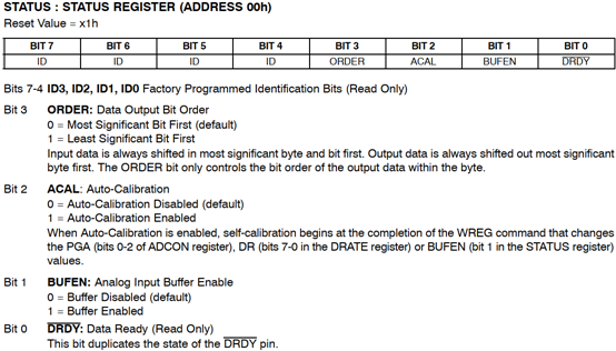
The configuration in the program is: buf [0] = (0 < < 3) | (1 < < 2) | (1 < < 1), which means LSB transmission, automatic calibration and analog input buffer.
- Set input channel parameters
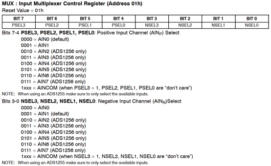
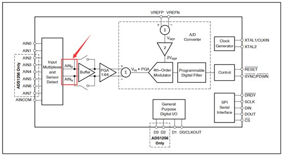
The configuration in the program is: buf[1] = 0x08, the upper four bits 0 represent AIN0 connected by AINp, and the lower four bits 8 represent AINCOM connected by AINn. AINp and AINn represent AIN0 of the current multiplexer gating:
- Set ADCON control register, which is mainly used for gain setting
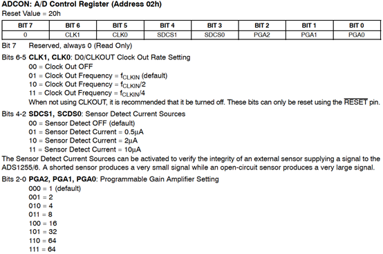
The configuration in the program is: buf [2] = (0 < < 5) | (0 < < 2) | (_gain < < 1), which means to turn off CLKOUT pin output, turn off sensor detection, and set the gain as a formal parameter_ gain.
- Set ADC sampling rate
The configuration in the program is: buf [3] = s_ Tabdatarate [#u drate], used to set baud rate:
static const uint8_t s_tabDataRate[ADS1256_DRATE_MAX] =
{
    0xF0,        /* Default value at reset */
    0xE0,
    0xD0,
    0xC0,
    0xB0,
    0xA1,
    0x92,
    0x82,
    0x72,
    0x63,
    0x53,
    0x43,
    0x33,
    0x20,
    0x13,
    0x03
};
typedef enum
{
    ADS1256_30000SPS = 0,
    ADS1256_15000SPS,
    ADS1256_7500SPS,
    ADS1256_3750SPS,
    ADS1256_2000SPS,
    ADS1256_1000SPS,
    ADS1256_500SPS,
    ADS1256_100SPS,
    ADS1256_60SPS,
    ADS1256_50SPS,
    ADS1256_30SPS,
    ADS1256_25SPS,
    ADS1256_15SPS,
    ADS1256_10SPS,
    ADS1256_5SPS,
    ADS1256_2d5SPS,

    ADS1256_DRATE_MAX
}ADS1256_DRATE_E;
93.5.5 in step 4, ADS1256 starts sampling
The code is implemented as follows
/*
*********************************************************************************************************
*    Function name: ADS1256_StartScan
*    Function Description: configure the DRDY pin (PC6) to the external interrupt trigger mode, and scan the data of 8 channels in the interrupt service program.
*    Formal parameters: None
*    Return value: None
*********************************************************************************************************
*/
void ADS1256_StartScan(void)
{
    /* PC6 External interrupt, BUSY
        Configure BUSY as the interrupt input port, and the falling edge is triggered */
    {
        GPIO_InitTypeDef   GPIO_InitStructure;

        DRDY_CLK_ENABLE();    /* Turn on GPIO clock */

        GPIO_InitStructure.Mode = GPIO_MODE_IT_FALLING;
        GPIO_InitStructure.Pull = GPIO_NOPULL;
        GPIO_InitStructure.Pin = DRDY_PIN;
        HAL_GPIO_Init(DRDY_GPIO, &GPIO_InitStructure);

        HAL_NVIC_SetPriority(DRDY_IRQn, 2, 0);
        HAL_NVIC_EnableIRQ(DRDY_IRQn);
    }

    /* Clear the result buffer before starting the scan */
    {
        uint8_t i;

        g_tADS1256.Channel = 0;

        for (i = 0; i < 8; i++)
        {
            g_tADS1256.AdcNow[i] = 0;
        }
    }
}
The code is relatively simple. It mainly configures the EXTI external interrupt of PC6 and initializes variables.
93.5.6 step 5: interrupt processing of ADS1256 (8-channel data reading)
The code is as follows:
/*
*********************************************************************************************************
*    Function name: EXTI9_5_IRQHandler
*    Function Description: external interrupt service program. The execution time of this program is about 123uS
*    Formal parameters: None
*    Return value: None
*********************************************************************************************************
*/
#ifdef EXTI9_ 5_ ISR_ MOVE_ This line is defined in out / * BSP. H, indicating that this function is moved to stam32f4xx_it.c.   Avoid duplicate definitions*/
void EXTI9_5_IRQHandler(void)
{
    HAL_GPIO_EXTI_IRQHandler(GPIO_PIN_6);
}

/*
*********************************************************************************************************
*    Function name: EXTI9_5_IRQHandler
*    Function Description: external interrupt service program entry. PI6 / AD7606_BUSY falling edge interrupt trigger
*    Formal parameters: None
*    Return value: None
*********************************************************************************************************
*/
void HAL_GPIO_EXTI_Callback(uint16_t GPIO_Pin)
{
    if (GPIO_Pin == GPIO_PIN_6)
    {

        ADS1256_ISR();
    }
}
#endif

/*
*********************************************************************************************************
*    Function name: ADS1256_ISR
*    Function Description: timing acquisition interrupt service program
*    Formal parameters: None
*    Return value: None
*********************************************************************************************************
*/
void ADS1256_ISR(void)
{
    /* Read the collection structure and save it in the global variable */
    ADS1256_SetChannal(g_tADS1256.Channel);    /* Switching analog channels */
    bsp_DelayUS(5);

    ADS1256_WriteCmd(CMD_SYNC);
    bsp_DelayUS(5);

    ADS1256_WriteCmd(CMD_WAKEUP);
    bsp_DelayUS(25);

    if (g_tADS1256.Channel == 0)
    {
        g_tADS1256.AdcNow[7] = ADS1256_ReadData();    /* Note that the data of the previous channel is saved */
    }
    else
    {
        g_tADS1256.AdcNow[g_tADS1256.Channel-1] = ADS1256_ReadData(); /* Note that the data of the previous channel is saved */
    }

    if (++g_tADS1256.Channel >= 8)
    {
        g_tADS1256.Channel = 0;
    }
}
The code of interrupt service program completely follows the following sequence:
- Step 1: ADS1256_ Setchannel (g_tads1256. Channel) switches the analog channel.
- Step 2: send SYNC synchronization command.
- Step 3: wake up.
- Step 4: read data.
In this process, pay special attention to reading the last converted data.
93.6 ADS1256 board level support package (bsp_spi_ads1256.c)
ADS1256 driver file bsp_spi_ads1256.c mainly implements the following API s for users to call:
- bsp_InitADS1256
- ADS1256_CfgADC
- ADS1256_StartScan
- ADS1256_SetChannal
- ADS1256_SetDiffChannal
93.6.1 function bsp_InitADS1256
Function prototype:
void bsp_InitADS1256(void)
Function Description:
It is mainly used for initialization of ADS1256.
93.6.2 function ADS1256_CfgADC
Function prototype:
void ADS1256_CfgADC(ADS1256_GAIN_E _gain, ADS1256_DRATE_E _drate)
Function Description:
Used to configure the gain and sampling rate of ADS1256.
Function parameters:
- The first parameter is used to set the gain. The supported parameters are as follows:
ADS1256_GAIN_1
ADS1256_GAIN_2
ADS1256_GAIN_4
ADS1256_GAIN_8
ADS1256_GAIN_16
ADS1256_GAIN_32
ADS1256_GAIN_64
- The second parameter is used to set the sampling rate. The supported parameters are as follows:
ADS1256_30000SPS
ADS1256_15000SPS
ADS1256_7500SPS
ADS1256_3750SPS
ADS1256_2000SPS
ADS1256_1000SPS
ADS1256_500SPS
ADS1256_100SPS
ADS1256_60SPS
ADS1256_50SPS
ADS1256_30SPS
ADS1256_25SPS
ADS1256_15SPS
ADS1256_10SPS
ADS1256_5SPS
ADS1256_2d5SPS
93.6.3 function ADS1256_StartScan
Function prototype:
void ADS1256_StartScan(void)
Function Description:
This function is used to start the interrupt mode of scanning and sampling.
93.6.4 function ADS1256_SetChannal
Function prototype:
static void ADS1256_SetChannal(uint8_t _ch)
Function Description:
This function sets the channel for single ended sampling.
Function parameters:
- The first parameter supports 0 to 7. 0 represents the sampling channel, 0, 1 represents the sampling channel, 1, and so on. The range is 0-7, a total of 8 channels.
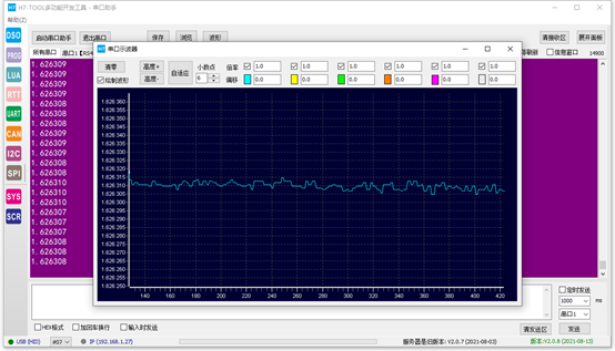
93.7 actual measurement effect of ADS1256 (10uV jitter)
Test LM285-2.5V voltage stabilizing effect, jitter 40uV:

Test the dry battery effect, and the jitter is about 10uV. Note that this level of jitter is easily affected by the ambient temperature, especially when the air conditioner is switched on and off.
93.8 ADS1256 driver transplantation and use
The migration steps are as follows:
- Step 1: copy bsp_spi_ads1256.c and bsp_spi_ads1256.h to your project directory and add it to the project.
- Step 2: modify BSP according to SPI pin, DRDY ready pin and RST reset pin used_ spi_ Macro definition starting with ADS1256. C.
/* Define GPIO ports */
#define SCK_CLK_ENABLE()     __HAL_RCC_GPIOA_CLK_ENABLE()
#define SCK_GPIO            GPIOA
#define SCK_PIN                GPIO_PIN_4
#define SCK_1()                SCK_GPIO->BSRR = SCK_PIN
#define SCK_0()                SCK_GPIO->BSRR = ((uint32_t)SCK_PIN << 16U)

#define DIN_CLK_ENABLE()     __HAL_RCC_GPIOG_CLK_ENABLE()
#define DIN_GPIO            GPIOG
#define DIN_PIN                GPIO_PIN_10
#define DIN_1()                DIN_GPIO->BSRR = DIN_PIN
#define DIN_0()                DIN_GPIO->BSRR = ((uint32_t)DIN_PIN << 16U)

#define CS_CLK_ENABLE()     __HAL_RCC_GPIOC_CLK_ENABLE()
#define CS_GPIO                GPIOC
#define CS_PIN                GPIO_PIN_7
#define CS_1()                CS_GPIO->BSRR = CS_PIN
#define CS_0()                CS_GPIO->BSRR = ((uint32_t)CS_PIN << 16U)

#define DOUT_CLK_ENABLE()     __HAL_RCC_GPIOA_CLK_ENABLE()
#define DOUT_GPIO            GPIOA
#define DOUT_PIN            GPIO_PIN_5
#define DOUT_IS_HIGH()        ((DOUT_GPIO->IDR & DOUT_PIN) != 0)

#define DRDY_CLK_ENABLE()     __HAL_RCC_GPIOC_CLK_ENABLE()
#define DRDY_GPIO            GPIOC
#define DRDY_PIN            GPIO_PIN_6
#define DRDY_IS_LOW()        ((DRDY_GPIO->IDR & DRDY_PIN) == 0)
#define DRDY_IRQn             EXTI9_5_IRQn
#define DRDY_IRQHandler        EXTI9_5_IRQHandler

/* PDWN  <------  PB7       Power down control */
#define PWDN_CLK_ENABLE()     __HAL_RCC_GPIOB_CLK_ENABLE()
#define PWDN_GPIO            GPIOB
#define PWDN_PIN            GPIO_PIN_7
#define PWDN_1()            PWDN_GPIO->BSRR = PWDN_PIN
#define PWDN_0()            PWDN_GPIO->BSRR = ((uint32_t)PWDN_PIN << 16U)

/*  RST   <------  PC3       Reset signal     */
#define RST_CLK_ENABLE()     __HAL_RCC_GPIOC_CLK_ENABLE()
#define RST_GPIO            GPIOC
#define RST_PIN                GPIO_PIN_3
#define RST_1()                RST_GPIO->BSRR = RST_PIN
#define RST_0()                RST_GPIO->BSRR = ((uint32_t)RST_PIN << 16U)
- Step 3: pay special attention that the entry of interrupt service program shall be modified according to the DRDY pin used.
/*
*********************************************************************************************************
*    Function name: EXTI9_5_IRQHandler
*    Function Description: external interrupt service program. The execution time of this program is about 123uS
*    Formal parameters: None
*    Return value: None
*********************************************************************************************************
*/
#ifdef EXTI9_ 5_ ISR_ MOVE_ This line is defined in out / * BSP. H, indicating that this function is moved to stam32f4xx_it.c.   Avoid duplicate definitions*/
void EXTI9_5_IRQHandler(void)
{
    HAL_GPIO_EXTI_IRQHandler(GPIO_PIN_6);
}

/*
*********************************************************************************************************
*    Function name: EXTI9_5_IRQHandler
*    Function Description: external interrupt service program entry. PI6 / AD7606_BUSY falling edge interrupt trigger
*    Formal parameters: None
*    Return value: None
*********************************************************************************************************
*/
void HAL_GPIO_EXTI_Callback(uint16_t GPIO_Pin)
{
    if (GPIO_Pin == GPIO_PIN_6)
    {

        ADS1256_ISR();
    }
}
#endif- Step 4: see the supporting examples in this chapter for the application method.
93.9 experimental routine design framework
Through the programming framework, we can have a comprehensive understanding of the supporting routines first, and then understand the details. The design framework of this experimental routine is as follows:
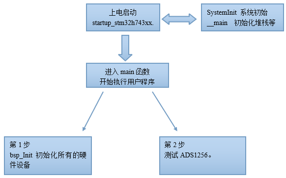
Phase 1, power on start-up phase:
- This part is described in detail in Chapter 14.
In stage 2, enter the main function:
- Part 1, hardware initialization, mainly including MPU, Cache, HAL library, system clock, tick timer and LED.
- Part 2, application design, test ADS1256.
93.10 experimental routine description (MDK)
Supporting examples:
V7-068_ADS1256 (8-channel 24 bit ADC with PGA)
Purpose of the experiment:
- Learn ADS1256, 8-Channel 24bit ADC with PGA.
Important:
- Please use external power supply for the development board.
Experiment content:
- Start an automatic software reinstallation timer and flip LED2 every 100ms.
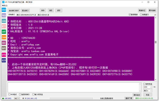
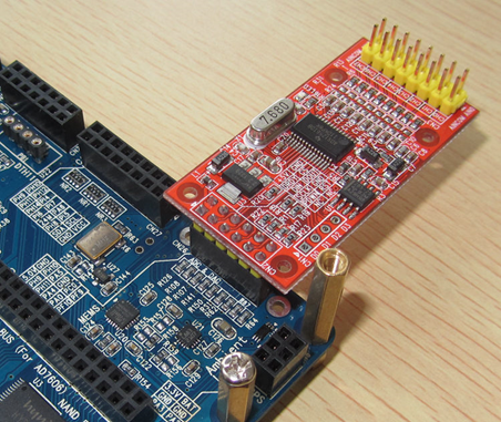
- After power on, insert ADS1256 module into CN26 (2*6P double row bus) in the upper right corner, and the program prints 8-channel sampling data every 1 second.
Information printed by serial port after power on:
Baud rate 115200, data bit 8, parity bit none, stop bit 1.
Module insertion position:

Programming:
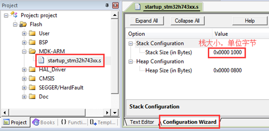
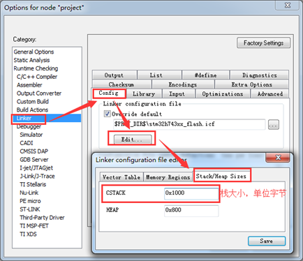
System stack size allocation:
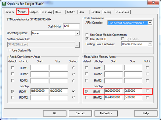
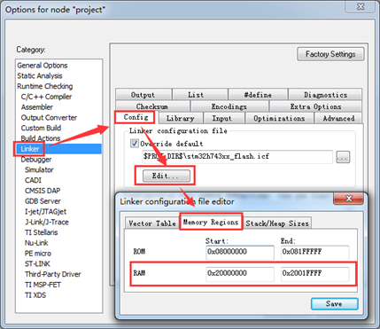
DTCM for RAM space:
Hardware peripheral initialization
The initialization of hardware peripherals is implemented in bsp.c file:
/*
*********************************************************************************************************
*    Function name: bsp_Init
*    Function Description: initialize all hardware devices. This function configures CPU registers and peripheral registers and initializes some global variables. You only need to call it once
*    Formal parameters: None
*    Return value: None
*********************************************************************************************************
*/
void bsp_Init(void)
{
    /* Configure MPU */
    MPU_Config();

    /* Enable L1 Cache */
    CPU_CACHE_Enable();

    /*
       STM32H7xx HAL During library initialization, the system still uses the 64MHz provided by H7. HSI clock:
       - Call function HAL_InitTick, initialize tick clock interrupt for 1ms.
       - Set NVIV priority grouping to 4.
     */
    HAL_Init();

    /*
       Configure the system clock to 400MHz
       - Switch to HSE.
       - This function updates the global variable systemcorelock and reconfigures HAL_InitTick.
    */
    SystemClock_Config();

    /*
       Event Recorder:
       - It can be used for code execution time measurement. It is only supported by MDK5.25 and above, but not IAR.
       - It is not enabled by default. If you want to enable this option, please refer to chapter xx of the V7 development board user manual
    */
#if Enable_EventRecorder == 1
    /* Initialize the EventRecorder and turn it on */
    EventRecorderInitialize(EventRecordAll, 1U);
    EventRecorderStart();
#endif

bsp_InitDWT();      /* Initialize DWT clock cycle counter */
    bsp_InitKey();         /* The key initialization should be placed before the tick timer, because the button detection is scanned by the tick timer */
    bsp_InitTimer();       /* Initialize tick timer */
    bsp_InitLPUart();     /* Initialize serial port */
    bsp_InitExtIO();     /* Initialize FMC bus 74HC574 extension IO. It must be in BSP_ Execute before initled() */
    bsp_InitLed();         /* Initialize LED */
bsp_InitExtSDRAM(); /* Initialize SDRAM */
}
MPU configuration and Cache configuration:
Both data Cache and instruction Cache are enabled. The AXI SRAM area (AXI SRAM is not used in this example) and the extended IO area of FMC are configured.
/*
*********************************************************************************************************
*    Function name: MPU_Config
*    Function Description: configure MPU
*    Formal parameters: None
*    Return value: None
*********************************************************************************************************
*/
static void MPU_Config( void )
{
    MPU_Region_InitTypeDef MPU_InitStruct;

    /* Disable MPU */
    HAL_MPU_Disable();

    /* Configure the MPU attribute of AXI SRAM as Write back, Read allocate, Write allocate */
    MPU_InitStruct.Enable           = MPU_REGION_ENABLE;
    MPU_InitStruct.BaseAddress      = 0x24000000;
    MPU_InitStruct.Size             = MPU_REGION_SIZE_512KB;
    MPU_InitStruct.AccessPermission = MPU_REGION_FULL_ACCESS;
    MPU_InitStruct.IsBufferable     = MPU_ACCESS_BUFFERABLE;
    MPU_InitStruct.IsCacheable      = MPU_ACCESS_CACHEABLE;
    MPU_InitStruct.IsShareable      = MPU_ACCESS_NOT_SHAREABLE;
    MPU_InitStruct.Number           = MPU_REGION_NUMBER0;
    MPU_InitStruct.TypeExtField     = MPU_TEX_LEVEL1;
    MPU_InitStruct.SubRegionDisable = 0x00;
    MPU_InitStruct.DisableExec      = MPU_INSTRUCTION_ACCESS_ENABLE;

    HAL_MPU_ConfigRegion(&MPU_InitStruct);


    /* Configure the MPU attribute of FMC extension IO as Device or Strongly Ordered */
    MPU_InitStruct.Enable           = MPU_REGION_ENABLE;
    MPU_InitStruct.BaseAddress      = 0x60000000;
    MPU_InitStruct.Size             = ARM_MPU_REGION_SIZE_64KB;
    MPU_InitStruct.AccessPermission = MPU_REGION_FULL_ACCESS;
    MPU_InitStruct.IsBufferable     = MPU_ACCESS_BUFFERABLE;
    MPU_InitStruct.IsCacheable      = MPU_ACCESS_NOT_CACHEABLE;
    MPU_InitStruct.IsShareable      = MPU_ACCESS_NOT_SHAREABLE;
    MPU_InitStruct.Number           = MPU_REGION_NUMBER1;
    MPU_InitStruct.TypeExtField     = MPU_TEX_LEVEL0;
    MPU_InitStruct.SubRegionDisable = 0x00;
    MPU_InitStruct.DisableExec      = MPU_INSTRUCTION_ACCESS_ENABLE;

    HAL_MPU_ConfigRegion(&MPU_InitStruct);

    /*Enable MPU */
    HAL_MPU_Enable(MPU_PRIVILEGED_DEFAULT);
}

/*
*********************************************************************************************************
*    Function name: CPU_CACHE_Enable
*    Function Description: enable L1 Cache
*    Formal parameters: None
*    Return value: None
*********************************************************************************************************
*/
static void CPU_CACHE_Enable(void)
{
    /* Enable I-Cache */
    SCB_EnableICache();

    /* Enable D-Cache */
    SCB_EnableDCache();
}
Call key processing every 10ms:
The key processing is realized in the tick timer interrupt, and the detection is performed every 10ms.
/*
*********************************************************************************************************
*    Function name: bsp_RunPer10ms
*    Function Description: this function is called by Systick interrupt every 10ms. See BSP for details_ Timer. C timing interrupt service program. Some processing time requirements
*              Lax tasks can be placed in this function. For example: key scanning, buzzer call control, etc.
*    Formal parameters: None
*    Return value: None
*********************************************************************************************************
*/
void bsp_RunPer10ms(void)
{
    bsp_KeyScan10ms();
}
Main functions:
The main program realizes the following operations:
- Start an automatic software reinstallation timer and flip LED2 every 100ms.
- After power on, insert ADS1256 module into CN26 (2*6P double row bus) in the upper right corner, and the program prints 8-channel sampling data every 1 second.
/*
*********************************************************************************************************
*    Function name: main
*    Function Description: c program entry
*    Formal parameters: None
*    Return value: error code (no processing required)
*********************************************************************************************************
*/
int main(void)
{
    uint8_t i;
    int32_t iTemp;
    float fTemp;


    bsp_Init();        /* Hardware initialization */
    PrintfLogo();    /* Print routine information to serial port 1 */

    PrintfHelp();    /* Print operation prompt information */


    bsp_DelayMS(500);    /* Wait for the power on to stabilize, wait for the reference voltage circuit to stabilize, bsp_InitADS1256() performs internal self calibration */

    bsp_InitADS1256();    /* Initialization configuration ADS1256. PGA = 1, drate = 30ksps, Bufen = 1, input positive and negative 5V */


    /* Print the chip ID (you can judge whether the hardware interface is normal by reading the ID). When it is normal, the high 4bit of the status register = 3 */
#if 0
    {
        uint8_t id;

        id = ADS1256_ReadChipID();

        if (id != 3)
        {
            printf("Error, ASD1256 Chip ID = 0x%X\r\n", id);
        }
        else
        {
            printf("Ok, ASD1256 Chip ID = 0x%X\r\n", id);
        }
    }
#endif

    ADS1256_CfgADC(ADS1256_GAIN_1, ADS1256_30SPS);    /* Configure ADC parameters: gain 1:1, data output rate 30Hz */

/* Start interrupt scanning mode and collect ADC data of 8 channels in turn. Through ADS1256_GetAdc() function to read the data */
    ADS1256_StartScan();

    bsp_StartAutoTimer(0, 1000);    /* Start a 100ms automatic reassembly timer */

    /* Enter the main program loop body */
    while (1)
    {
        bsp_Idle();        /* This function is in the bsp.c file. Users can modify this function to realize CPU sleep and dog feeding */


        if (bsp_CheckTimer(0))    /* Judge timer timeout */
        {
            /* Come in every 1000ms */
            bsp_LedToggle(2);    /* Flip LED status */

            /* Print collected data */
            for (i = 0; i < 8; i++)
            {

                  /*
                    Calculation formula: 2 * VREF/(PGA * (2^23 - 1)), where VREF is 2.5V and PGA = 1
                  */
                   /* Calculate the actual voltage value (approximately estimated), and calibrate it for accuracy */
                iTemp = ((int64_t)g_tADS1256.AdcNow[i] * 2500000) / 4194303;


                fTemp = (float)iTemp / 1000000;

                printf("CH%d=%07d(%fV) ", i, g_tADS1256.AdcNow[i], fTemp);

                if(i == 3)
                {
                    printf("\r\n");
                }
            }

            printf("\r\n\r\n");
        }
    }
}
93.11 experimental routine description (IAR)
Supporting examples:
V7-068_ADS1256 (8-channel 24 bit ADC with PGA)
Purpose of the experiment:
- Learn ADS1256, 8-Channel 24bit ADC with PGA.
Important:
- Please use external power supply for the development board.
Experiment content:
- Start an automatic software reinstallation timer and flip LED2 every 100ms.
- After power on, insert ADS1256 module into CN26 (2*6P double row bus) in the upper right corner, and the program prints 8-channel sampling data every 1 second.
Information printed by serial port after power on:
Baud rate 115200, data bit 8, parity bit none, stop bit 1.

Module insertion position:
Programming:
System stack size allocation:
DTCM for RAM space:
Hardware peripheral initialization
The initialization of hardware peripherals is implemented in bsp.c file:
/*
*********************************************************************************************************
*    Function name: bsp_Init
*    Function Description: initialize all hardware devices. This function configures CPU registers and peripheral registers and initializes some global variables. You only need to call it once
*    Formal parameters: None
*    Return value: None
*********************************************************************************************************
*/
void bsp_Init(void)
{
    /* Configure MPU */
    MPU_Config();

    /* Enable L1 Cache */
    CPU_CACHE_Enable();

    /*
       STM32H7xx HAL During library initialization, the system still uses the 64MHz provided by H7. HSI clock:
       - Call function HAL_InitTick, initialize tick clock interrupt for 1ms.
       - Set NVIV priority grouping to 4.
     */
    HAL_Init();

    /*
       Configure the system clock to 400MHz
       - Switch to HSE.
       - This function updates the global variable systemcorelock and reconfigures HAL_InitTick.
    */
    SystemClock_Config();

    /*
       Event Recorder:
       - It can be used for code execution time measurement. It is only supported by MDK5.25 and above, but not IAR.
       - It is not enabled by default. If you want to enable this option, please refer to chapter xx of the V7 development board user manual
    */
#if Enable_EventRecorder == 1
    /* Initialize the EventRecorder and turn it on */
    EventRecorderInitialize(EventRecordAll, 1U);
    EventRecorderStart();
#endif

bsp_InitDWT();      /* Initialize DWT clock cycle counter */
    bsp_InitKey();         /* The key initialization should be placed before the tick timer, because the button detection is scanned by the tick timer */
    bsp_InitTimer();       /* Initialize tick timer */
    bsp_InitLPUart();     /* Initialize serial port */
    bsp_InitExtIO();     /* Initialize FMC bus 74HC574 extension IO. It must be in BSP_ Execute before initled() */
    bsp_InitLed();         /* Initialize LED */
bsp_InitExtSDRAM(); /* Initialize SDRAM */

    /* For different applications, add the required underlying driver module initialization function */
    bsp_InitAD7606();    /* Configure GPIO for AD7606 */
}
MPU configuration and Cache configuration:
Both data Cache and instruction Cache are enabled. The AXI SRAM area (AXI SRAM is not used in this example) and the extended IO area of FMC are configured.
/*
*********************************************************************************************************
*    Function name: MPU_Config
*    Function Description: configure MPU
*    Formal parameters: None
*    Return value: None
*********************************************************************************************************
*/
static void MPU_Config( void )
{
    MPU_Region_InitTypeDef MPU_InitStruct;

    /* Disable MPU */
    HAL_MPU_Disable();

    /* Configure the MPU attribute of AXI SRAM as Write back, Read allocate, Write allocate */
    MPU_InitStruct.Enable           = MPU_REGION_ENABLE;
    MPU_InitStruct.BaseAddress      = 0x24000000;
    MPU_InitStruct.Size             = MPU_REGION_SIZE_512KB;
    MPU_InitStruct.AccessPermission = MPU_REGION_FULL_ACCESS;
    MPU_InitStruct.IsBufferable     = MPU_ACCESS_BUFFERABLE;
    MPU_InitStruct.IsCacheable      = MPU_ACCESS_CACHEABLE;
    MPU_InitStruct.IsShareable      = MPU_ACCESS_NOT_SHAREABLE;
    MPU_InitStruct.Number           = MPU_REGION_NUMBER0;
    MPU_InitStruct.TypeExtField     = MPU_TEX_LEVEL1;
    MPU_InitStruct.SubRegionDisable = 0x00;
    MPU_InitStruct.DisableExec      = MPU_INSTRUCTION_ACCESS_ENABLE;

    HAL_MPU_ConfigRegion(&MPU_InitStruct);


    /* Configure the MPU attribute of FMC extension IO as Device or Strongly Ordered */
    MPU_InitStruct.Enable           = MPU_REGION_ENABLE;
    MPU_InitStruct.BaseAddress      = 0x60000000;
    MPU_InitStruct.Size             = ARM_MPU_REGION_SIZE_64KB;
    MPU_InitStruct.AccessPermission = MPU_REGION_FULL_ACCESS;
    MPU_InitStruct.IsBufferable     = MPU_ACCESS_BUFFERABLE;
    MPU_InitStruct.IsCacheable      = MPU_ACCESS_NOT_CACHEABLE;
    MPU_InitStruct.IsShareable      = MPU_ACCESS_NOT_SHAREABLE;
    MPU_InitStruct.Number           = MPU_REGION_NUMBER1;
    MPU_InitStruct.TypeExtField     = MPU_TEX_LEVEL0;
    MPU_InitStruct.SubRegionDisable = 0x00;
    MPU_InitStruct.DisableExec      = MPU_INSTRUCTION_ACCESS_ENABLE;

    HAL_MPU_ConfigRegion(&MPU_InitStruct);

    /*Enable MPU */
    HAL_MPU_Enable(MPU_PRIVILEGED_DEFAULT);
}

/*
*********************************************************************************************************
*    Function name: CPU_CACHE_Enable
*    Function Description: enable L1 Cache
*    Formal parameters: None
*    Return value: None
*********************************************************************************************************
*/
static void CPU_CACHE_Enable(void)
{
    /* Enable I-Cache */
    SCB_EnableICache();

    /* Enable D-Cache */
    SCB_EnableDCache();
}
Call key processing every 10ms:
The key processing is realized in the tick timer interrupt, and the detection is performed every 10ms.
/*
*********************************************************************************************************
*    Function name: bsp_RunPer10ms
*    Function Description: this function is called by Systick interrupt every 10ms. See BSP for details_ Timer. C timing interrupt service program. Some processing time requirements
*              Lax tasks can be placed in this function. For example: key scanning, buzzer call control, etc.
*    Formal parameters: None
*    Return value: None
*********************************************************************************************************
*/
void bsp_RunPer10ms(void)
{
    bsp_KeyScan10ms();
}
Main functions:
The main program realizes the following operations:
- Start an automatic software reinstallation timer and flip LED2 every 100ms.
- After power on, insert ADS1256 module into CN26 (2*6P double row bus) in the upper right corner, and the program prints 8-channel sampling data every 1 second.
/*
*********************************************************************************************************
*    Function name: main
*    Function Description: c program entry
*    Formal parameters: None
*    Return value: error code (no processing required)
*********************************************************************************************************
*/
int main(void)
{
    uint8_t i;
    int32_t iTemp;
    float fTemp;


    bsp_Init();        /* Hardware initialization */
    PrintfLogo();    /* Print routine information to serial port 1 */

    PrintfHelp();    /* Print operation prompt information */


    bsp_DelayMS(500);    /* Wait for the power on to stabilize, wait for the reference voltage circuit to stabilize, bsp_InitADS1256() performs internal self calibration */

    bsp_InitADS1256();    /* Initialization configuration ADS1256. PGA = 1, drate = 30ksps, Bufen = 1, input positive and negative 5V */


    /* Print the chip ID (you can judge whether the hardware interface is normal by reading the ID). When it is normal, the high 4bit of the status register = 3 */
#if 0
    {
        uint8_t id;

        id = ADS1256_ReadChipID();

        if (id != 3)
        {
            printf("Error, ASD1256 Chip ID = 0x%X\r\n", id);
        }
        else
        {
            printf("Ok, ASD1256 Chip ID = 0x%X\r\n", id);
        }
    }
#endif

    ADS1256_CfgADC(ADS1256_GAIN_1, ADS1256_30SPS);    /* Configure ADC parameters: gain 1:1, data output rate 30Hz */

/* Start interrupt scanning mode and collect ADC data of 8 channels in turn. Through ADS1256_GetAdc() function to read the data */
    ADS1256_StartScan();

    bsp_StartAutoTimer(0, 1000);    /* Start a 100ms automatic reassembly timer */

    /* Enter the main program loop body */
    while (1)
    {
        bsp_Idle();        /* This function is in the bsp.c file. Users can modify this function to realize CPU sleep and dog feeding */


        if (bsp_CheckTimer(0))    /* Judge timer timeout */
        {
            /* Come in every 1000ms */
            bsp_LedToggle(2);    /* Flip LED status */

            /* Print collected data */
            for (i = 0; i < 8; i++)
            {

                  /*
                    Calculation formula: 2 * VREF/(PGA * (2^23 - 1)), where VREF is 2.5V and PGA = 1
                  */
                   /* Calculate the actual voltage value (approximately estimated), and calibrate it for accuracy */
                iTemp = ((int64_t)g_tADS1256.AdcNow[i] * 2500000) / 4194303;


                fTemp = (float)iTemp / 1000000;

                printf("CH%d=%07d(%fV) ", i, g_tADS1256.AdcNow[i], fTemp);

                if(i == 3)
                {
                    printf("\r\n");
                }
            }

            printf("\r\n\r\n");
        }
    }
}
93.12 summary
This chapter involves a lot of knowledge. It mainly explains the common playing methods of ADS1256. If this chip is used in an actual project, it needs to be skillfully used.