1) Experimental platform: ZYNQ development board of punctual atomic navigator
2) Platform purchase address: https://item.taobao.com/item.htm?&id=606160108761
3) Full set of experimental source code + manual + video download address: http://www.openedv.com/thread-301505-1-1.html
4) Students interested in punctual atomic FPGA can add group discussion: 994244016
5) pay attention to the official account of the dot atom and get updated information.

Chapter 21 HDMI color bar display experiment
HDMI interface has been widely used in consumer electronics industry, such as computers, LCD TVs, projectors and other products. Some professional video devices such as cameras and video switchers also integrate HDMI interfaces. In this chapter, we will learn how to drive the HDMI interface on the pioneer development board.
This chapter includes the following parts:
21.1 introduction
21.2 experimental tasks
21.3 hardware design
21.4 program design
21.5 download verification
21.1 introduction
HDMI is a new generation of multimedia interface standard. Its full English name is high definition multimedia interface, that is, HD multimedia interface. It can transmit video and audio at the same time, simplifying the interface and connection of the equipment; At the same time, it provides higher data transmission bandwidth and can transmit uncompressed digital audio and high-resolution video signals. HDMI version 1.0 was released in 2002, and the maximum data transmission speed is 5Gbps; The theoretical bandwidth of HDMI 2.1 standard released in 2017 can reach 48Gbps.
Before the emergence of HDMI interface, VGA interface was widely used. The full name of VGA is Video Graphics Array, that is, Video Graphics Array. It is a standard for video transmission using analog signals. VGA interface adopts 15 pin structure, which transmits analog signal, color component, synchronization and other signals. It is the interface used by many old graphics cards, notebooks and projectors. Because the VGA interface transmits analog signals, its signals are easy to be disturbed. Therefore, the VGA font is easy to be false under high resolution. If the signal line is long, the image will be tailed. VGA interface is shown in the figure below:
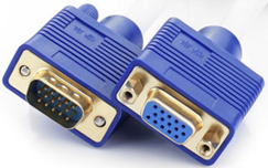
Figure 7.5.13.1 VGA interface
In addition to the signal being easily disturbed, the VGA interface is also large. Therefore, the VGA interface has gradually withdrawn from the stage, and some displays are no longer equipped with VGA interface. Today, with the high development of digital equipment, HDMI interface and DP (Display Port) interface are replaced.
HDMI is downward compatible with DVI, but DVI (digital video interface) can only be used to transmit video, not audio at the same time, which is the main difference between the two. In addition, the size of DVI interface is significantly larger than that of HDMI interface, as shown in the following figure:
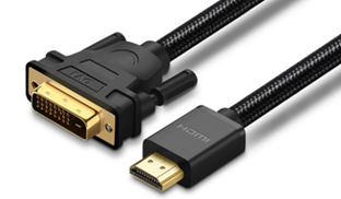
Figure 7.5.13.2 physical diagram of DVI interface (left) and HDMI interface (right)
Figure 7.5.13.2 on the right is the most common type A HDMI interface in life, and its pin definition is shown in the following figure:
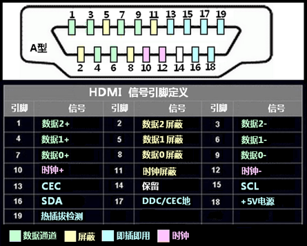
Figure 7.5.13.3 definition of HDMI interface pin
DVI and HDMI interface protocols use TMDS standard to transmit audio and video data in the physical layer. TMDS (Transition Minimized Differential Signaling) is a high-speed data transmission technology developed by Silicon Image company in the United States. Differential signals are used to transmit high-speed serial data in DVI and HDMI video interfaces. TMDS differential transmission technology uses two pins (such as "data 2 +" and "data 2 -" in figure 7.5.13.3) to transmit a signal. The positive and negative polarity and size of the voltage difference between the two pins are used to determine the value of transmitted data (0 or 1).
Xilnx adds support for TMDS interface standard to devices after Spartan-3A series, which is used to realize DVI and HDMI interfaces within FPGA.
Because this experiment only uses HDMI interface to display images and does not need to transmit audio, we only need to realize the driving logic of DVI interface. However, before that, we need to briefly understand the TMDS video transmission protocol.
Figure 7.5.13.4 is the connection diagram of TMDs transmitting end and receiving end. The TMDS connection used for DVI or HDMI video transmission is realized through four serial channels. For DVI, three channels are used to transmit the red, green and blue color components of each pixel in the video (RGB 4:4:4 format). HDMI also uses three RGB channels by default, but it can also choose to transmit the brightness and chroma information of pixels (YCrCb 4:4:4 or YCrCb 4:2:2 format). The fourth channel is the clock channel, which is used to transmit the pixel clock. The independent TMDs clock channel provides the receiving reference frequency for the receiving end to ensure the correct recovery of data at the receiving end.
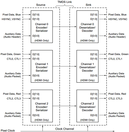
Figure 7.5.13.4 TMDS connection diagram
If the color depth of each pixel is 24 bits, that is, each RGB color component occupies 8 bits, the color data on each channel will be converted into a 10 bit pixel character through an 8B/10B Encoder. Then the 10 bit character is converted into serial data through the Serializer, and finally sent out by the TMDS data channel. The serial data rate generated by this 10:1 parallel to serial process is 10 times the actual pixel clock rate.
In the process of video image transmission, the encoded effective pixel characters are transmitted on the data channel. In the time interval (blanking period) between lines of each frame image and between different frames in the video, the control characters are transmitted on the data channel. Each channel has an input interface of two control signals, corresponding to four different control characters. These control characters provide line synchronization (HSYNC) and frame synchronization (VSYNC) information of video, and can also be used to specify the boundary of transmitted data (for synchronization).
For DVI transmission, the whole blanking period of video is used to transmit control characters. In addition to the control characters, the blanking period of HDMI transmission can also be used to transmit audio or other additional data, such as caption information. This is the main difference between DVI and HDMI protocols. This difference can also be seen from figure 7.5.13.4, that is, the "Auxiliary Data" interface is marked with "HDMI Olny", that is, it is a unique interface of HDMI.
From the previous introduction, we can see that TMDS connection can be logically divided into two stages: encoding and parallel serial conversion. In the encoding stage, the encoder encodes the pixel data in the video source, the audio / additional data of HDMI, and the line synchronization and field synchronization signals into 10 bit character streams respectively. Then, in the parallel serial conversion stage, the above character stream is converted into a serial data stream and sent out from three differential output channels.
The DVI encoder outputs pixel data in the video effective data segment and control data in the blanking period, as shown in figure 7.5.13.5. Where VDE (Video Data Enable) is a high level, indicating that the video data is valid, and it is a low level, indicating that it is currently in the video blanking period.
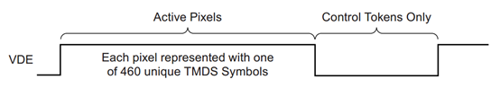
Figure 7.5.13.5 schematic diagram of DVI coding output
Figure 7.5.13.6 shows the schematic diagram of three channel DVI encoder. For the three RGB color channels of pixel data, the logic of the encoder is exactly the same. VDE is used for each channel to select whether to output video pixel data or control data. HSYNC and VSYNC signals are encoded in the blue channel to obtain 10 characters, and then transmitted in the video blanking period. The control signals C0 and C1 of the green and red channels also need to be encoded and output in the blanking period. However, in the DVI specification, the control signals of these two channels are reserved (not used), so they are set to 2'b00.
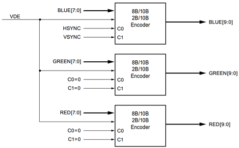
Figure 7.5.13.6 schematic diagram of DVI encoder
The video pixel data input by each channel shall be encoded by TMDS coding algorithm in DVI specification. Each 8-bit data will be converted into one of 460 specific 10 bit characters. This coding mechanism roughly realizes the DC balance in the transmission process, that is, the number of high-level (digital "1") transmitted in a period of time is roughly equal to the number of low-level (digital "0"). At the same time, the number of state jumps ("from 1 to 0" or "from 0 to 1") in each encoded 10 bit character will be limited to five times.
In addition to video data, the state of 2-bit control signal of each channel shall also be encoded. After encoding, it corresponds to four different 10 bit control characters, namely 10 'b1101010100, 10' b00101011, 10 'b01010100, and 10' b1010101011. It can be seen that each control character has more than seven state jumps. The difference in the number of state jumps between video characters and control characters will be used for the synchronization of transmitting and receiving devices.
HDMI protocol and DVI protocol are the same in many aspects, including physical connection (TMDS), effective video coding algorithm and the definition of control characters. However, compared with DVI, HDMI transmits more data during the blanking period of video, including audio data and additional data. 4-bit audio and additional data will be converted into 10 bit TERC4 characters through TERC4 encoding mechanism, and then transmitted on green and red channels.
When HDMI inputs additional data, it also needs to input ADE (Aux/Audio Data Enable) signal. Its function is similar to VDE: when ADE is at high level, it indicates that the additional data or audio data at the input end is valid. If you want to know more about HDMI, please refer to the HDMI interface specification - High Definition Multimedia Interface Specification Version 1.3A in the development board materials (disk a) / software materials. For simplicity, here we drive the HDMI interface as a DVI interface.
After encoding, the 10 bit characters of the three channels will be converted into parallel series, which is realized by using the special hardware resources in the 7-series FPGA. ZYNQ PL part is equivalent to 7 Series FPGA. It provides a special parallel serial converter - OSERDESE2. A single OSERDESE2 module can realize 8:1 parallel serial conversion, and 10:1 and 14:1 conversion rates can be realized through bit width expansion.
21.2 experimental tasks
The experimental task of this chapter is to drive the HDMI interface on the pilot ZYNQ development board to display the color bar pattern on the display.
21.3 hardware design
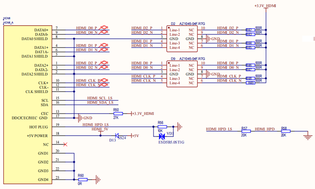
Figure 7.5.13.1 schematic diagram of HDMI interface 1
Figure 7.5.13.1 is a part of the pilot ZYNQ backplane HDMI interface schematic diagram, in which three data channels of HDMI are HDMI_D[2:0] to and one clock channel HDMI_CLK is directly connected to the TMDS differential pin at the PL end of ZYNQ.
HDMI_HPD refers to Hot Plug Detect. When the video device is connected with the receiving device through HDMI, the receiving device sets the HPD to high level and notifies the transmitting device. When the transmitting device detects that the HPD is low, it indicates that the connection is disconnected.
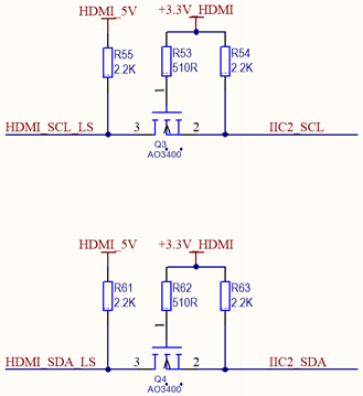
Figure 7.5.13.2 schematic diagram of HDMI interface 2
In figure 7.5.13.2, HDMI_SCL_LS and HDMI_SDA_LS is the Display Data Channel (DDC) of HDMI interface, which is used to exchange some configuration information between HDMI sender and receiver and communicate through I2C protocol. The sending end reads the EDID data saved in the HDMI display EEPROM at the receiving end through the DDC channel, obtains the information of the receiving end, confirms the settings and functions displayed at the receiving end, and determines the format of audio / video data transmission with the receiving end.
Only TMDS data and TMDS clock signal of HDMI interface are used in this experiment. The pin allocation of each port is shown in the table below:
Table 21.3.1 pin allocation of HDMI color bar display experiment
Signal name direction pin port description level standard
sys_clk input U18 system clock, 50M LVCMOS33
sys_rst_n input N16 system reset, low effective LVCMOS33
tmds_data_p[2] output J20 TMDS data channel 2 (positive) TMDs_ thirty-three
tmds_data_p[1] output K19 TMDS data channel 1 (positive) TMDs_ thirty-three
tmds_data_p[0] output G19 TMDS data channel 0 (positive) TMDs_ thirty-three
tmds_clk_p output J18 TMDS clock channel (positive)_ thirty-three
It should be noted that TMDS data and clock signals need to specify the level standard as TMDS in the constraint file_ 33. In addition, for differential signals, we only need to specify the pin position of the positive pole, and the tool will automatically allocate the pin of the negative pole.
The related pin constraints are as follows:
#System clock and reset
set_property -dict {PACKAGE_PIN U18  IOSTANDARD LVCMOS33} [get_ports sys_clk]
set_property -dict {PACKAGE_PIN N16  IOSTANDARD LVCMOS33} [get_ports sys_rst_n]

#HDMI
set_property -dict {PACKAGE_PIN J20  IOSTANDARD TMDS_33 } [get_ports {tmds_data_p[2]}]
set_property -dict {PACKAGE_PIN K19  IOSTANDARD TMDS_33 } [get_ports {tmds_data_p[1]}]
set_property -dict {PACKAGE_PIN G19  IOSTANDARD TMDS_33 } [get_ports {tmds_data_p[0]}]
set_property -dict {PACKAGE_PIN J18  IOSTANDARD TMDS_33 } [get_ports tmds_clk_p]
21.4 program design
Because this experiment only needs to display images through HDMI interface, it is driven as DVI interface. In addition, we only need to realize the image sending function. The system block diagram of this experiment is as follows:
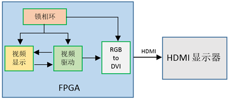
Figure 7.5.13.1 system block diagram
This experiment adds an RGB2DVI module based on the LCD color bar display experiment to convert the video image in RGB888 format into TMDS data output. This chapter focuses on the introduction of RGB2DVI module. For the introduction of other modules, please refer to the LCD color bar display experiment.
The design block diagram of RGB2DVI top-level module is as follows:
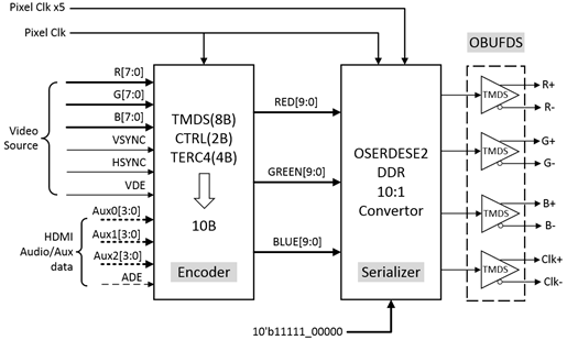
Figure 7.5.13.2 block diagram of rgb2dvi module
In figure 7.5.13.2, the Encoder module is responsible for encoding the data, and the Serializer module performs parallel serial conversion on the encoded data, and finally converts it into TMDS differential signal transmission through OBUFDS.
The whole system needs two input clocks, one is the pixel clock Pixel Clk of the video, and the other clock Pixel Clk x5 has a frequency five times that of the pixel clock. From the previous introduction, we know that the parallel serial conversion process realizes a conversion rate of 10:1. Theoretically, the converter needs a serial clock with a frequency of 10 times the pixel clock frequency. Here we only use a clock frequency of 5 times, because OSERDESE2 module can realize the function of DDR, that is, it realizes double data rate on the basis of 5 times the clock frequency.
The clock channel connected to TMDs is realized by using the same parallel to serial logic as the data channel. Through the 10 bit binary sequence 10'b11111_ If 00000 performs parallel serial conversion at 10 times the pixel clock frequency, the TMDS reference clock at the pixel clock frequency can be obtained.
In addition, it should be noted that the audio / additional data input of HDMI at the lower left foot in the figure is not used in this experiment, so it is represented by a dotted line.
First, let's look at the code of the Encoder module:
1   `timescale 1 ps / 1ps
2
3   module dvi_encoder (
4     input            clkin,    // pixel clock input
5     input            rstin,    // async. reset input (active high)
6     input      [7:0] din,      // data inputs: expect registered
7     input            c0,       // c0 input
8     input            c1,       // c1 input
9     input            de,       // de input
10    output reg [9:0] dout      // data outputs
11  );
12
13
14    // Counting number of 1s and 0s for each incoming pixel
15    // component. Pipe line the result.
16    // Register Data Input so it matches the pipe lined adder
17    // output
18
19    reg [3:0] n1d; //number of 1s in din
20    reg [7:0] din_q;
21
22  //Calculate the number of "1" in pixel data
23    always @ (posedge clkin) begin
24      n1d <=#1 din[0]+din[1]+din[2]+din[3]+din[4]+din[5]+din[6]+din[7];
25
26      din_q <=#1 din;
27    end
28
29    ///
30    // Stage 1: 8 bit -> 9 bit
31    // Refer to DVI 1.0 Specification, page 29, Figure 3-5
32    ///
33    wire decision1;
34
35    assign decision1 = (n1d > 4'h4) | ((n1d == 4'h4) & (din_q[0] == 1'b0));
36
37    wire [8:0] q_m;
38    assign q_m[0] = din_q[0];
39    assign q_m[1] = (decision1) ? (q_m[0] ^~ din_q[1]) : (q_m[0] ^ din_q[1]);
40    assign q_m[2] = (decision1) ? (q_m[1] ^~ din_q[2]) : (q_m[1] ^ din_q[2]);
41    assign q_m[3] = (decision1) ? (q_m[2] ^~ din_q[3]) : (q_m[2] ^ din_q[3]);
42    assign q_m[4] = (decision1) ? (q_m[3] ^~ din_q[4]) : (q_m[3] ^ din_q[4]);
43    assign q_m[5] = (decision1) ? (q_m[4] ^~ din_q[5]) : (q_m[4] ^ din_q[5]);
44    assign q_m[6] = (decision1) ? (q_m[5] ^~ din_q[6]) : (q_m[5] ^ din_q[6]);
45    assign q_m[7] = (decision1) ? (q_m[6] ^~ din_q[7]) : (q_m[6] ^ din_q[7]);
46    assign q_m[8] = (decision1) ? 1'b0 : 1'b1;
47
48    /
49    // Stage 2: 9 bit -> 10 bit
50    // Refer to DVI 1.0 Specification, page 29, Figure 3-5
51    /
52    reg [3:0] n1q_m, n0q_m; // number of 1s and 0s for q_m
53    always @ (posedge clkin) begin
54      n1q_m  <=#1 q_m[0]+q_m[1]+q_m[2]+q_m[3]+q_m[4]+q_m[5]+q_m[6]+q_m[7];
55      n0q_m  <=#1 4'h8 - (q_m[0]+q_m[1]+q_m[2]+q_m[3]+q_m[4]+q_m[5]+q_m[6]+q_m[7]);
56    end
57
58    parameter CTRLTOKEN0 = 10'b1101010100;
59    parameter CTRLTOKEN1 = 10'b0010101011;
60    parameter CTRLTOKEN2 = 10'b0101010100;
61    parameter CTRLTOKEN3 = 10'b1010101011;
62
63    reg [4:0] cnt; //disparity counter, MSB is the sign bit
64    wire decision2, decision3;
65
66    assign decision2 = (cnt == 5'h0) | (n1q_m == n0q_m);
67    /
68    // [(cnt > 0) and (N1q_m > N0q_m)] or [(cnt < 0) and (N0q_m > N1q_m)]
69    /
70    assign decision3 = (~cnt[4] & (n1q_m > n0q_m)) | (cnt[4] & (n0q_m > n1q_m));
71
72
73    // pipe line alignment
74
75    reg       de_q, de_reg;
76    reg       c0_q, c1_q;
77    reg       c0_reg, c1_reg;
78    reg [8:0] q_m_reg;
79
80    always @ (posedge clkin) begin
81      de_q    <=#1 de;
82      de_reg  <=#1 de_q;
83
84      c0_q    <=#1 c0;
85      c0_reg  <=#1 c0_q;
86      c1_q    <=#1 c1;
87      c1_reg  <=#1 c1_q;
88
89      q_m_reg <=#1 q_m;
90    end
91
92    ///
93    // 10-bit out
94    // disparity counter
95    ///
96    always @ (posedge clkin or posedge rstin) begin
97      if(rstin) begin
98        dout <= 10'h0;
99        cnt <= 5'h0;
100     end else begin
101       if (de_reg) begin
102         if(decision2) begin
103           dout[9]   <=#1 ~q_m_reg[8];
104           dout[8]   <=#1 q_m_reg[8];
105           dout[7:0] <=#1 (q_m_reg[8]) ? q_m_reg[7:0] : ~q_m_reg[7:0];
106
107           cnt <=#1 (~q_m_reg[8]) ? (cnt + n0q_m - n1q_m) : (cnt + n1q_m - n0q_m);
108         end else begin
109           if(decision3) begin
110             dout[9]   <=#1 1'b1;
111             dout[8]   <=#1 q_m_reg[8];
112             dout[7:0] <=#1 ~q_m_reg[7:0];
113
114             cnt <=#1 cnt + {q_m_reg[8], 1'b0} + (n0q_m - n1q_m);
115           end else begin
116             dout[9]   <=#1 1'b0;
117             dout[8]   <=#1 q_m_reg[8];
118             dout[7:0] <=#1 q_m_reg[7:0];
119
120             cnt <=#1 cnt - {~q_m_reg[8], 1'b0} + (n1q_m - n0q_m);
121           end
122         end
123       end else begin
124         case ({c1_reg, c0_reg})
125           2'b00:   dout <=#1 CTRLTOKEN0;
126           2'b01:   dout <=#1 CTRLTOKEN1;
127           2'b10:   dout <=#1 CTRLTOKEN2;
128           default: dout <=#1 CTRLTOKEN3;
129         endcase
130
131         cnt <=#1 5'h0;
132       end
133     end
134   end
135
136 endmodule
dvi_ The encoder module encodes the input 8-bit pixel data and 2-bit line field synchronization signal according to the TMDS coding algorithm in the DVI interface specification. This module is the coding module provided in Xilinx application note XAPP460. The specific coding algorithm is shown in the following figure:
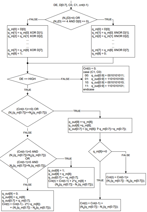
Figure 7.5.13.3 TMDS coding algorithm
TMDS encodes 8-bit character data into 10 bit character data through minimum conversion through logic algorithm. The first 8 bits of data are obtained after operation from the original signal. The 9th bit represents the operation mode, 1 represents XOR and 0 represents XOR and non. After DC balance (bit 10), differential signal is used to transmit data. Bit 10 is actually an inversion flag bit. 1 indicates that inversion has been performed and 0 indicates no inversion, so as to achieve DC balance.
After receiving the signal, the receiving end performs the opposite operation. TMDS has better EMC performance than LVDS and TTL. This algorithm can reduce the overshoot and undershoot in the process of signal transmission, and DC balance can reduce the electromagnetic interference of the signal to the transmission line. It can realize long-distance and high-quality digital signal transmission with low-cost special cable.
The algorithm described in figure 7.5.13.3 is defined by the DVI interface specification. We will not conduct in-depth research. If you are interested, you can also compare it with DVI_ The code in the encoder module to analyze how the whole algorithm process is implemented using Verilog. The meaning of each parameter in the algorithm is shown in the following figure:
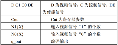
Figure 7.5.13.4 parameters of TMDs coding algorithm
The data encoded by TMDS is subjected to parallel serial conversion by the Serializer module, and the code is as follows:
1   `timescale 1ns / 1ps
2
3   module serializer_10_to_1(
4       input           reset,              // Reset, high effective
5       input           paralell_clk,       // Input parallel data clock
6       input           serial_clk_5x,      // Input serial data clock
7       input   [9:0]   paralell_data,      // Input parallel data
8
9       output          serial_data_out     // Output serial data
10      );
11
12  //wire define
13  wire        cascade1;     //Signals for cascading two OSERDESE2
14  wire        cascade2;
15
16  //*****************************************************
17  //**                    main code
18  //*****************************************************
19
20  //Instantiate OSERDESE2 primitive to realize parallel serial conversion and Master mode
21  OSERDESE2 #(
22      .DATA_RATE_OQ   ("DDR"),        // Set double data rate
23      .DATA_RATE_TQ   ("SDR"),        // DDR, BUF, SDR
24      .DATA_WIDTH     (10),           // The input parallel data width is 10bit
25      .SERDES_MODE    ("MASTER"),     // Set to Master for 10bit width expansion
26      .TBYTE_CTL      ("FALSE"),      // Enable tristate byte operation (FALSE, TRUE)
27      .TBYTE_SRC      ("FALSE"),      // Tristate byte source (FALSE, TRUE)
28      .TRISTATE_WIDTH (1)             // 3-state converter width (1,4)
29  )
30  OSERDESE2_Master (
31      .CLK        (serial_clk_5x),    // Serial data clock, 5x clock frequency
32      .CLKDIV     (paralell_clk),     // Parallel data clock
33      .RST        (reset),            // 1-bit input: Reset
34      .OCE        (1'b1),             // 1-bit input: Output data clock enable
35
36      .OQ         (serial_data_out),  // Serial output data
37
38      .D1         (paralell_data[0]), // D1 - D8: parallel data input
39      .D2         (paralell_data[1]),
40      .D3         (paralell_data[2]),
41      .D4         (paralell_data[3]),
42      .D5         (paralell_data[4]),
43      .D6         (paralell_data[5]),
44      .D7         (paralell_data[6]),
45      .D8         (paralell_data[7]),
46
47      .SHIFTIN1   (cascade1),         // SHIFTIN1 for bit width extension
48      .SHIFTIN2   (cascade2),         // SHIFTIN2
49      .SHIFTOUT1  (),                 // SHIFTOUT1: used for bit width extension
50      .SHIFTOUT2  (),                 // SHIFTOUT2
51
52      .OFB        (),                 // The following are unused signals
53      .T1         (1'b0),
54      .T2         (1'b0),
55      .T3         (1'b0),
56      .T4         (1'b0),
57      .TBYTEIN    (1'b0),
58      .TCE        (1'b0),
59      .TBYTEOUT   (),
60      .TFB        (),
61      .TQ         ()
62  );
63
64  //Instantiate OSERDESE2 primitive to realize parallel serial conversion and Slave mode
65  OSERDESE2 #(
66      .DATA_RATE_OQ   ("DDR"),        // Set double data rate
67      .DATA_RATE_TQ   ("SDR"),        // DDR, BUF, SDR
68      .DATA_WIDTH     (10),           // The input parallel data width is 10bit
69      .SERDES_MODE    ("SLAVE"),      // Set to Slave for 10bit width expansion
70      .TBYTE_CTL      ("FALSE"),      // Enable tristate byte operation (FALSE, TRUE)
71      .TBYTE_SRC      ("FALSE"),      // Tristate byte source (FALSE, TRUE)
72      .TRISTATE_WIDTH (1)             // 3-state converter width (1,4)
73  )
74  OSERDESE2_Slave (
75      .CLK        (serial_clk_5x),    // Serial data clock, 5x clock frequency
76      .CLKDIV     (paralell_clk),     // Parallel data clock
77      .RST        (reset),            // 1-bit input: Reset
78      .OCE        (1'b1),             // 1-bit input: Output data clock enable
79
80      .OQ         (),                 // Serial output data
81
82      .D1         (1'b0),             // D1 - D8: parallel data input
83      .D2         (1'b0),
84      .D3         (paralell_data[8]),
85      .D4         (paralell_data[9]),
86      .D5         (1'b0),
87      .D6         (1'b0),
88      .D7         (1'b0),
89      .D8         (1'b0),
90
91      .SHIFTIN1   (),                 // SHIFTIN1 for bit width extension
92      .SHIFTIN2   (),                 // SHIFTIN2
93      .SHIFTOUT1  (cascade1),         // SHIFTOUT1: used for bit width extension
94      .SHIFTOUT2  (cascade2),         // SHIFTOUT2
95
96      .OFB        (),                 // The following are unused signals
97      .T1         (1'b0),
98      .T2         (1'b0),
99      .T3         (1'b0),
100     .T4         (1'b0),
101     .TBYTEIN    (1'b0),
102     .TCE        (1'b0),
103     .TBYTEOUT   (),
104     .TFB        (),
105     .TQ         ()
106 );
107
108 endmodule
serdes_10_to_1 module realizes 10:1 parallel serial conversion by calling OSERDESE2 primitive. Primitives are functional modules in the underlying hardware of Xilinx devices, which use dedicated resources to realize a series of functions. Compared with IP core, the calling method of primitive is simpler, but it is generally only used to realize some simple functions.
It should be noted that an OSERDESE2 can only achieve a conversion rate of 8:1 at most. Here, we realize 10:1 parallel serial conversion through bit width expansion, as shown in the figure below:
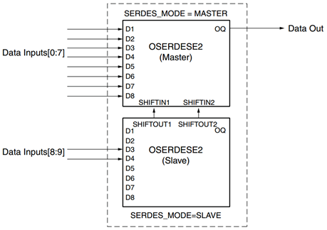
Figure 7.5.13.5 oserde2 bit width extension
As shown in figure 7.5.13.5, OSERDESE2 bit width expansion is realized through two OSERDESE2 modules, one as Master and the other as Slave. In this way, 14:1 parallel serial conversion can be realized at most. It should be noted that only D3 to D8 can be used at the data input of the Slave module during bit width expansion.
Finally, we call the above two modules in the RGB2DVI top-level module, which is shown in the following code:
1   module dvi_transmitter_top(
2       input        pclk,           // pixel clock
3       input        pclk_x5,        // pixel clock x5
4       input        reset_n,        // reset
5
6       input [23:0] video_din,      // RGB888 video in
7       input        video_hsync,    // hsync data
8       input        video_vsync,    // vsync data
9       input        video_de,       // data enable
10
11      output       tmds_clk_p,     // TMDS clock channel
12      output       tmds_clk_n,
13      output [2:0] tmds_data_p,    // TMDS data channel
14      output [2:0] tmds_data_n,
15      output       tmds_oen        // TMDS output enable
16      );
17
18  //wire define
19  wire        reset;
20
21  //parallel data
22  wire [9:0]  red_10bit;
23  wire [9:0]  green_10bit;
24  wire [9:0]  blue_10bit;
25  wire [9:0]  clk_10bit;
26
27  //serial data
28  wire [2:0]  tmds_data_serial;
29  wire        tmds_clk_serial;
30
31  //*****************************************************
32  //**                    main code
33  //*****************************************************
34  assign tmds_oen = 1'b1;
35  assign clk_10bit = 10'b1111100000;
36
37  //Asynchronous reset, synchronous release
38  asyn_rst_syn reset_syn(
39      .reset_n    (reset_n),
40      .clk        (pclk),
41
42      .syn_reset  (reset)    //Highly effective
43      );
44
45  //Encodes three color channels
46  dvi_encoder encoder_b (
47      .clkin      (pclk),
48      .rstin      (reset),
49
50      .din        (video_din[7:0]),
51      .c0         (video_hsync),
52      .c1         (video_vsync),
53      .de         (video_de),
54      .dout       (blue_10bit)
55      ) ;
56
57  dvi_encoder encoder_g (
58      .clkin      (pclk),
59      .rstin      (reset),
60
61      .din        (video_din[15:8]),
62      .c0         (1'b0),
63      .c1         (1'b0),
64      .de         (video_de),
65      .dout       (green_10bit)
66      ) ;
67
68  dvi_encoder encoder_r (
69      .clkin      (pclk),
70      .rstin      (reset),
71
72      .din        (video_din[23:16]),
73      .c0         (1'b0),
74      .c1         (1'b0),
75      .de         (video_de),
76      .dout       (red_10bit)
77      ) ;
78
79  //Parallel serial conversion of encoded data
80  serializer_10_to_1 serializer_b(
81      .reset              (reset),                // Reset, high effective
82      .paralell_clk       (pclk),                 // Input parallel data clock
83      .serial_clk_5x      (pclk_x5),              // Input serial data clock
84      .paralell_data      (blue_10bit),           // Input parallel data
85
86      .serial_data_out    (tmds_data_serial[0])   // Output serial data
87      );
88
89  serializer_10_to_1 serializer_g(
90      .reset              (reset),
91      .paralell_clk       (pclk),
92      .serial_clk_5x      (pclk_x5),
93      .paralell_data      (green_10bit),
94
95      .serial_data_out    (tmds_data_serial[1])
96      );
97
98  serializer_10_to_1 serializer_r(
99      .reset              (reset),
100     .paralell_clk       (pclk),
101     .serial_clk_5x      (pclk_x5),
102     .paralell_data      (red_10bit),
103
104     .serial_data_out    (tmds_data_serial[2])
105     );
106
107 serializer_10_to_1 serializer_clk(
108     .reset              (reset),
109     .paralell_clk       (pclk),
110     .serial_clk_5x      (pclk_x5),
111     .paralell_data      (clk_10bit),
112
113     .serial_data_out    (tmds_clk_serial)
114     );
115
116 //Convert differential signal
117 OBUFDS #(
118     .IOSTANDARD         ("TMDS_33")    // The I/O level standard is TMDS
119 ) TMDS0 (
120     .I                  (tmds_data_serial[0]),
121     .O                  (tmds_data_p[0]),
122     .OB                 (tmds_data_n[0])
123     );
124
125 OBUFDS #(
126     .IOSTANDARD         ("TMDS_33")    // The I/O level standard is TMDS
127 ) TMDS1 (
128     .I                  (tmds_data_serial[1]),
129     .O                  (tmds_data_p[1]),
130     .OB                 (tmds_data_n[1])
131     );
132
133 OBUFDS #(
134     .IOSTANDARD         ("TMDS_33")    // The I/O level standard is TMDS
135 ) TMDS2 (
136     .I                  (tmds_data_serial[2]),
137     .O                  (tmds_data_p[2]),
138     .OB                 (tmds_data_n[2])
139     );
140
141 OBUFDS #(
142     .IOSTANDARD         ("TMDS_33")    // The I/O level standard is TMDS
143 ) TMDS3 (
144     .I                  (tmds_clk_serial),
145     .O                  (tmds_clk_p),
146     .OB                 (tmds_clk_n)
147     );
148
149 endmodule
On DVI_ transmitter_ In the top module, not only the coding module and parallel to serial module are instantiated, but also four OBUFDS primitives are instantiated to convert three channels of data and one channel of clock signal into differential signal output, as shown in lines 116 to 147 of the program.
OBUFDS is a differential output buffer, which is used to convert signals from FPGA internal logic into differential signal output, and supports TMDS level standard. The schematic diagram of OBUFDS primitive is as follows:
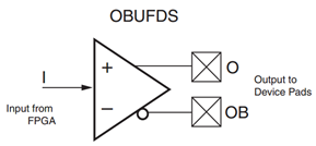
Figure 7.5.13.6 schematic diagram of obufds primitive
In lines 37 to 43 of the program, asyn is instantiated_ rst_ Syn module. The OSERDESE2 module requires that the high level of the reset signal is valid, and the asynchronous reset signal needs to be synchronized to the serial clock domain. So we're at asyn_ rst_ The syn module converts the low-level effective asynchronous reset signal into high-level effective, and carries out asynchronous reset and synchronous release processing at the same time.
asyn_ rst_ The code of syn module is as follows:
1  module asyn_rst_syn(
2      input clk,          //Destination clock domain
3      input reset_n,      //Asynchronous reset, low effective
4
5      output syn_reset    //Highly effective
6      );
7
8  //reg define
9  reg reset_1;
10 reg reset_2;
11
12 //*****************************************************
13 //**                    main code
14 //*****************************************************
15 assign syn_reset  = reset_2;
16
17 //Synchronously release the asynchronous reset signal and convert it to high effective
18 always @ (posedge clk or negedge reset_n) begin
19     if(!reset_n) begin
20         reset_1 <= 1'b1;
21         reset_2 <= 1'b1;
22     end
23     else begin
24         reset_1 <= 1'b0;
25         reset_2 <= reset_1;
26     end
27 end
28
29 endmodule
It can be seen that the code of this module is very simple, which is equivalent to registering the input asynchronous reset signal connection twice in the clock domain requiring synchronization. This is a very common method for synchronizing asynchronous signals. It should be noted that in the always block on line 18 of the program, the function of converting a low-level effective reset signal into a high-level effective reset signal is also realized.
Here, the program design of RGB2DVI module is introduced. The schematic diagram of the whole module is as follows:
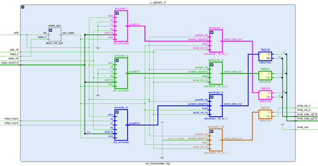
Figure 7.5.13.7 schematic diagram of rgb2dvi module
In figure 7.5.13.2, we use red / Green / blue to identify the input video data video respectively_ There are three different color channels in din. It can also be seen from the figure that the processing process of each color channel is the same, all of which go through DVI first_ Encoder, and then serializer_ 10_ to_ Module 1 performs parallel serial conversion, and finally converts it into TMDS differential signal through OBUFDS primitive.
Next, we call the RGB2DVI module in the top-level module of the whole system and export the color bar pattern through the HDMI interface.
The top module of the system is hdmi_colorbar_top, the code is as follows:
1  module  hdmi_colorbar_top(
2      input        sys_clk,
3      input        sys_rst_n,
4
5      output       tmds_clk_p,    // TMDS clock channel
6      output       tmds_clk_n,
7      output [2:0] tmds_data_p,   // TMDS data channel
8      output [2:0] tmds_data_n
9  );
10
11 //wire define
12 wire          pixel_clk;
13 wire          pixel_clk_5x;
14 wire          clk_locked;
15
16 wire  [10:0]  pixel_xpos_w;
17 wire  [10:0]  pixel_ypos_w;
18 wire  [23:0]  pixel_data_w;
19
20 wire          video_hs;
21 wire          video_vs;
22 wire          video_de;
23 wire  [23:0]  video_rgb;
24
25 //*****************************************************
26 //**                    main code
27 //*****************************************************
28
29 //Instantiated MMCM/PLL IP core
30 clk_wiz_0  clk_wiz_0(
31     .clk_in1        (sys_clk),
32     .clk_out1       (pixel_clk),        //Pixel clock
33     .clk_out2       (pixel_clk_5x),     //5x pixel clock
34
35     .reset          (~sys_rst_n),
36     .locked         (clk_locked)
37 );
38
39 //Example video display driver module
40 video_driver u_video_driver(
41     .pixel_clk      (pixel_clk),
42     .sys_rst_n      (sys_rst_n),
43
44     .video_hs       (video_hs),
45     .video_vs       (video_vs),
46     .video_de       (video_de),
47     .video_rgb      (video_rgb),
48
49     .pixel_xpos     (pixel_xpos_w),
50     .pixel_ypos     (pixel_ypos_w),
51     .pixel_data     (pixel_data_w)
52     );
53
54 //Example video display module
55 video_display  u_video_display(
56     .pixel_clk      (pixel_clk),
57     .sys_rst_n      (sys_rst_n),
58
59     .pixel_xpos     (pixel_xpos_w),
60     .pixel_ypos     (pixel_ypos_w),
61     .pixel_data     (pixel_data_w)
62     );
63
64 //Exemplary HDMI driver module
65 dvi_transmitter_top u_rgb2dvi_0(
66     .pclk           (pixel_clk),
67     .pclk_x5        (pixel_clk_5x),
68     .reset_n        (sys_rst_n & clk_locked),
69
70     .video_din      (video_rgb),
71     .video_hsync    (video_hs),
72     .video_vsync    (video_vs),
73     .video_de       (video_de),
74
75     .tmds_clk_p     (tmds_clk_p),
76     .tmds_clk_n     (tmds_clk_n),
77     .tmds_data_p    (tmds_data_p),
78     .tmds_data_n    (tmds_data_n),
79     .tmds_oen       ()                        //The reserved port is not used in this experiment
80     );
81
82 endmodule
In lines 30 to 37 of the code, we generate two clocks by calling the clock IP core, including pixel_clk is the pixel clock, while pixel_clk_5x is the serial data clock required by the parallel serial conversion module, and its frequency is pixel_ Five times CLK.
In the top-level module, video_ The display module (line 55) is responsible for generating color bar patterns in RGB888 format, and then displaying them in video_ Driven by the driver module (line 40), the video signal, line field synchronization signal and video effective signal are output according to the VGA display timing of the industrial standard. These signals are used as the input of RGB2DVI module (line 65), and finally converted into TMDS serial data of DVI/HDMI interface standard and output to HDMI interface.
Video in the above code_ Display module and video_driver module and LCD in the implementation of LCD color bar display_ Driver and LCD_ The display module is almost identical. If you are not familiar with these two modules, please refer to LCD color bar display experiment.
Top level module HDMI_ colorbar_ The schematic diagram of top is as follows:
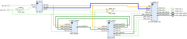
Figure 7.5.13.8 schematic diagram of top-level module
In figure 7.5.13.8, the orange line is the pixel clock pixel_clk, the clock signal is connected to all other modules. The blue line is the serial data clock pixel_clk_5x, the clock signal is only connected to the RGB2DVI module.
21.5 download verification
First, we connect the downloader to the JTAG interface on the navigator's backplane, and the other end of the Downloader is connected to the computer. Then use the HDMI cable to connect the HDMI display to the HDMI connector on the pilot backplane. Finally, connect the power supply of the development board and turn on the power switch, as shown in the figure below:

Figure 7.5.13.1 connection diagram of pilot development board
Then we download the BIT file generated in this experiment to the development board. After downloading, the color bar pattern is displayed on the HDMI display, indicating that the experiment is successfully downloaded and verified on the pilot ZYNQ development board.
The experimental results are shown in the figure below:
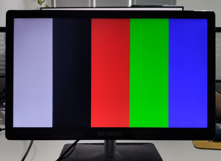
Fig. 7.5.13.2 experimental results