Reference: use based on STM32 OLED (IIC)
Author: struggling little Yin
Release time: 2021-05-07 13:09:26
website: https://blog.csdn.net/boybs/article/details/116465668
IIC introduction
IIC protocol introduction
IIC communication protocol (inter integrated circuit) is developed by Phiips Philips. Due to its few pins, simple hardware implementation and strong scalability, it does not need UASRT (ch340 is required for level conversion at serial port) and external transceiver of CAN communication protocol, Now it is widely used in the communication between multiple integrated circuit ICs (chips) in the system (chip level communication generally uses IIC communication).
IIC is half duplex communication mode (SPI is full duplex, with faster speed, but more lines)
SDA: data cable
SCL: clock line
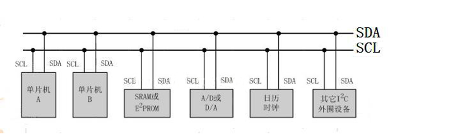
IIC bus system structure
-
The project is a bus that supports multiple devices. " "Bus" refers to the signal line shared by multiple devices. In an IIC communication bus, multiple IIC communication devices (127 at most) can be connected at the same time, supporting multiple communication hosts and multiple communication slaves.
-
An IIC bus of the project only uses two bus lines, one bidirectional serial data line (SDA) and one serial clock line (SCL). The data line is used to represent data, and the clock line is used for data transceiver synchronization.
-
Each device connected to the bus has an independent address, which can be used by the host for direct access to different devices.
Characteristics of IIC bus physical layer
-
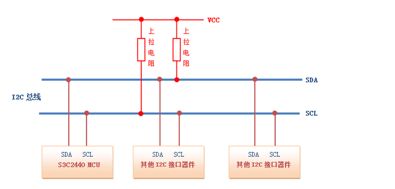
The bus is connected to the power supply through a pull-up resistor. When the IIC device is idle, it will output the high resistance state (the resistance is very large, which is equivalent to disconnection, as mentioned in the four output modes of GPIO earlier). When all devices are idle, they will output the high resistance state, and the pull-up resistance will pull the bus to high level.
-
When multiple hosts use the bus at the same time, in order to prevent data conflict, arbitration mode (CAN bus is similar to MCU interrupt priority) will be used to determine which device occupies the bus.
-
There are three transmission modes: the standard mode has a transmission rate of 100kbit/s, the fast mode is 400kbit/s, and the high-speed mode can reach 3.4M/s. However, most IIC devices do not support the high-speed mode at present.
Hardware IIC, software IIC
Hardware IIC: the IIC peripherals on the corresponding chip have corresponding IIC drive circuits, and the IIC pins used are also special (similar PA9 and PA10 are specially used for receiving and transmitting serial ports)
Software IIC: generally, ordinary GPIO pins are used to control pin status and simulate IIC communication waveform to realize the function of IIC
difference:
The efficiency of hardware IIC is much higher than that of software (special hardware driver circuits are integrated), while software IIC is not limited by pins (which pin you want to use for IIC communication), and the interface is more flexible.
Software IIC simulates the working mode of registers through GPIO, while hardware IIC directly calls internal registers for configuration. If you want to look at the specific hardware, you can go to the chip manual. Because the port of firmware IIC is fixed, it will be different.
How to distinguish?
1. The usage of hardware IIC is complex, and the simulation IIC process is clearer
2. Hardware IIC is faster than simulation, and DMA can be used (DMA is a channel, so you don't need to know much at present)
3. The analog iic can be on any pin, and the hardware IIC is on the fixed pin
IIC communication protocol layer
IIC protocol layer
IIC protocol defines the start and stop signals, data validity, response, arbitration, clock synchronization and address broadcasting of communication.
The host (single chip microcomputer) writes data to the slave (peripheral)
The shaded part represents the signal sent by the host to the slave
The white part represents the signal sent from the slave to the host
-
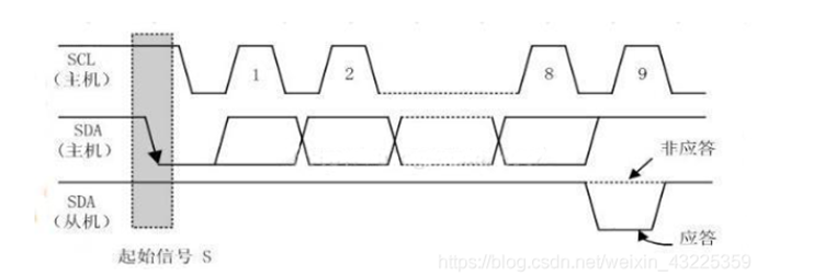
S: Data is transmitted from the master to the slave (a start signal)
-
SLAVE ADDRESS: after the start signal is generated, all slaves begin to broadcast the SLAVE ADDRESS signal immediately after the start signal. IIC bus, the address of each device is unique. When the address broadcast by the host is the same as that of a device, the device is selected, and the unselected device will ignore the subsequent data signal. According to the IIC protocol, the SLAVE ADDRESS can be 7 bits or 10 bits.
-
R/W (read / write) transmission direction selection bit, 0: indicates that the data transmission direction is transmitted from the host to the slave, that is, the host writes data to the slave. Is 1: the opposite is true.
-
P: End of data transmission
-
After the slave receives the transmission direction selection bit, the host or slave returns a reply (ACK a above) or non reply (NACK A / a above) signal. Only after receiving the reply signal can the host continue to send or receive data.
Write data from the slave (peripheral) to the host (single chip microcomputer)
The shaded part represents the signal sent by the host to the slave
The white part represents the signal sent from the slave to the host
Host reads slave data:
The configuration direction transmission bit is "read data" direction (host read). After broadcasting the address and receiving the response signal, the slave starts to return data (DATA) to the host. The packet size is also 8 bits. Each time the slave sends a number, it will wait for the response signal (ACK) of the host. Repeat this process to return n data. N has no size limit. When the host wants to stop receiving data, it returns a non response signal (NCAK) to the slave, and the slave automatically stops data transmission.
Communication composite format
The shaded part represents the signal sent by the host to the slave
The white part represents the signal sent from the slave to the host
In the composite format, there are two start signals (S) in the transmission process. In the first transmission process, the host passes slave_ After address finds the slave device, it sends a section of "data", which is usually used to represent the internal register or memory address of the slave device; In the second transmission, the contents of the address are read or written. In other words, the first communication is to tell the slave to read and write the address, and the second is to read and write the actual content.
IIC communication process
① Idle state
② Start signal
③ Stop signal
④ Response signal
⑤ Validity of data
⑥ Data transmission
① Idle state
SDA and SCL signal lines of IIC bus are at high level at the same time, and the idle state of bit bus is specified. At this time, the output stage FET of each device is in the cut-off state, that is, the bus is released, and the level is raised by the respective pull-up resistors of the two signal lines.
② Start signal ③ stop signal
Start signal: when SCL is high level, SDA has high to low jump; The start signal is a level jump timing signal, not a level signal.
Stop signal: when SCL is high, SDA jumps from low to high; The stop signal is also a high-level jump timing signal, not a level signal.
The serial port also has a start signal and a stop signal, but the serial port is not synchronized
The start signal and stop signal are generally generated by the host
④ Response signal
Every time the transmitter sends a byte (a byte is 8 bits), the data line is released during clock pulse 9 (as shown in the figure below), and a reply signal is fed back by the receiver. The reply signal is at low level and is specified as effective reply bit (ACK bit for short), indicating that the receiver has successfully received the byte; The reply signal is high level and is specified as non reply bit (NACK), which generally indicates that the receiver failed to receive the byte.
The requirement for feedback effective answer bit ACK is that the receiver pulls the SDA line low during the low level before the ninth clock pulse and ensures a stable low level during the high level of the clock.
If the receiver is the master, after it receives the last byte, it sends a NACK signal to notify the controlled transmitter of data transmission, and releases the SDA line so that the master receiver sends a stop signal P.
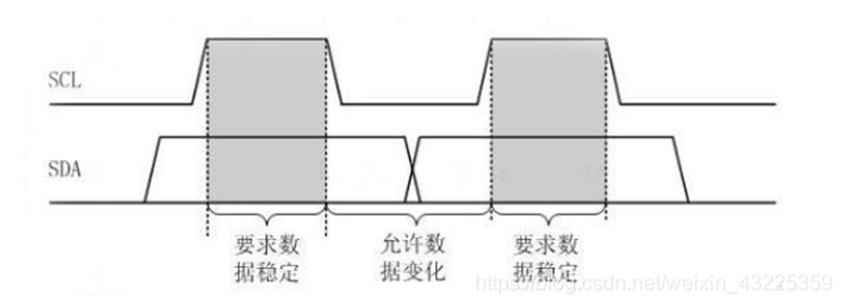
⑤ Validity of data
When the IIC bus transmits data, the data on the data line must remain stable during the period when the clock signal is high level. Only during the period when the signal on the clock line is low level, the high level or low level state on the data line is allowed to change. The SDA data line transmits one bit of data in each clock cycle of SCL.
That is, the data should be ready before the rising edge of SCL. And must stabilize before the falling edge
⑥ Data transmission
Each bit of data transmitted on IIC bus has a clock pulse corresponding (or synchronous control), that is, with the cooperation of SCL serial clock, each bit of data is transmitted bit by bit on SDA. The transmission of data bits is edge triggered.
IIC characteristics and architecture of STM32
① Software simulation protocol: use CPU to directly control the level of communication pin to generate logic that meets the communication protocol standard. It has strong portability and is used most.
② Hardware implementation protocol: the IIC on-chip peripheral of STM32 is specially responsible for implementing the IIC communication protocol (). As long as the peripheral is configured, it will automatically generate communication signals according to the protocol requirements, send and receive data and cache it. As long as the CPU detects the status of the peripheral and accesses the data register, it can complete data sending and receiving. This way of processing IIC protocol by hardware peripherals reduces the work of CPU and makes the software design simpler (it feels very similar to timer / counter).
In any case, the chip will always need some external devices to implement a certain system. In order to distinguish from those peripherals, it will be integrated into the chip, but it does not belong to the chip itself (such as DSP, which is a microprocessor, so the parts of the chip that do not belong to the microprocessor are peripherals)
The IIC peripheral of STM32 can be used as the master and slave of communication, supports the rates of 100Kbit/s and 400Kbits/s, supports 7-bit and 10 bit device addresses, supports DMA data transmission, and has the function of data verification.
Among them, SMBA: data transmission mode, starting from high or low.
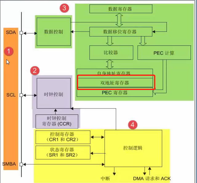
1. Communication pin
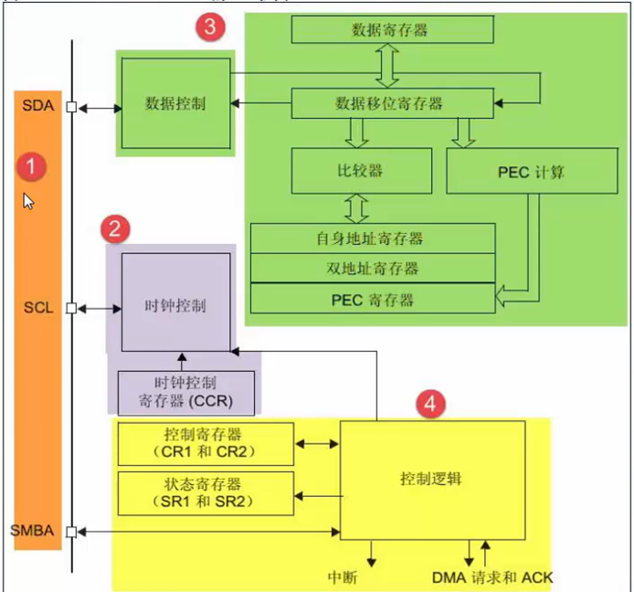
STM32 chip has multiple IIC peripherals, and their IIC communication signals are led out to different GPIO pins. These specified pins (hardware IIC) must be configured when using. There are three groups of peripheral IIC pins in the figure below. If we use software mode, any IO port can be used as IIC communication interface.
2. Clock control logic
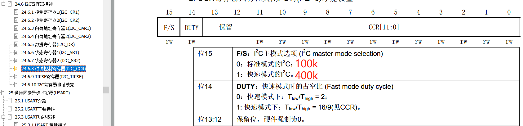
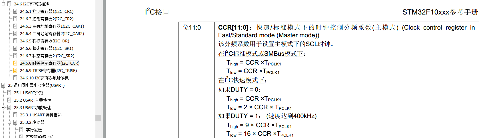
The clock signal of the SCL line is controlled by the IIC interface according to the clock control register (CCR), and the controlled parameter is the main bit clock frequency.
-
The "standard / fast" mode of IIC communication can be selected, and the two modes correspond to the communication rate of 100/400Kbits/s respectively.
-
In the fast mode, the duty cycle of SCL clock can be selected, and T(low)/T(high) = 2 or T(low)/T(high)=16/9 mode can be selected (as shown in the figure below).
-
The 12 bit configuration factor CCR in the CCR register shares the function with the input clock source of IIC peripheral to generate SCL clock. IIC peripheral input clock source bit PCKL1 of STM32
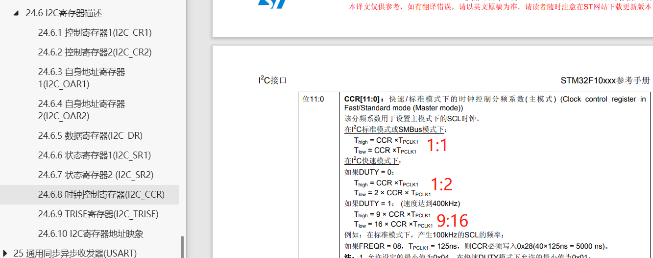
Calculate clock frequency (value of CCR)
-
Standard mode
T high = CCR* Tpckl1
T low= CCR* Tpclk1 -
When TLOW / thingh = 2 in fast mode:
Thigh = CCR* Tpckl1
Tlow = 2* low* Tpckl1 -
When Tlow/Thigh =16/9 in fast mode:
Thigh = 9* CCR* Tpckl1
Tlow = 16* low* Tpckl1
For example (when Tlow/Thigh =2 in fast mode): PCLK1 = 36MHz (the frequency of AHB1 bus is a dichotomy). To configure 400Kbits/s method:
PCLK clock cycle: TPCLK1 = 1/36 000 000
Target SCL clock cycle: TSCL = 1/400 000
High level time in SCL clock cycle: Thigh = TSCL/3
Low level time in SCL clock cycle: Tlow = 2*TSCL/3
Calculate the value of CCR: CCR = height / tpclk1 = 30
The calculated value can be written to the register
3. Data control logic
The SDA signal of IIC is mainly connected to the data shift register. The data source and target of the data shift register are data register (DR), address register (OAR), PEC register and SDA data line.
When sending data outward, the data shift register takes the "data register" as the data source and sends the data bit by bit through the SDA signal line (the SMBA mentioned above controls the transmission sequence and starts from the high bit).
When receiving data from the outside, the data shift register stores the data sampled by the SDA signal line bit by bit in the "data register".
When IIC peripheral is used for communication, it will write parameters to different data bits of "status register (SR1 and SR2)" at different stages of communication, and understand the communication status by reading these register flags.
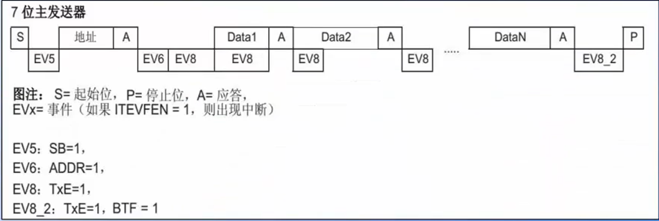
Main transmitter
-
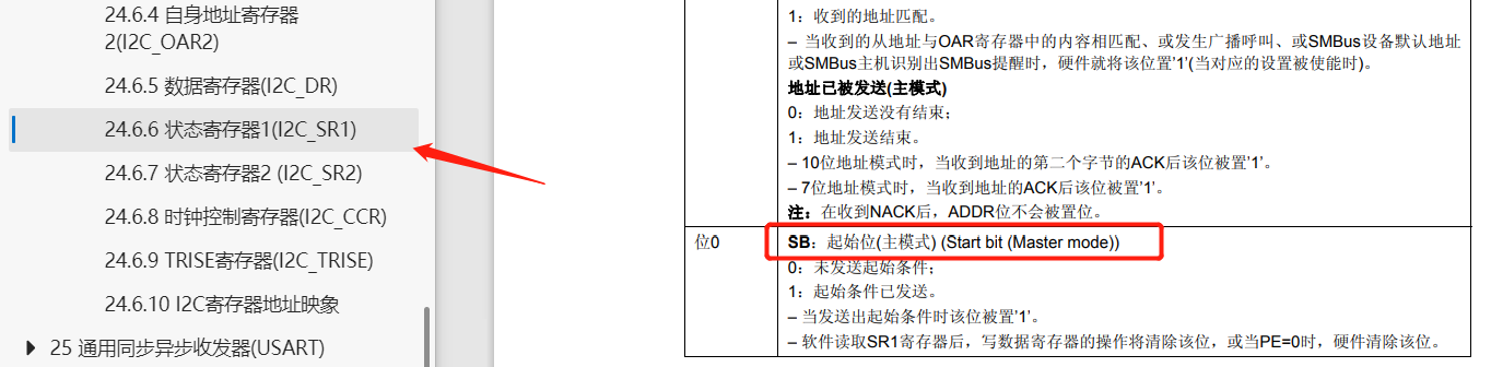
The control generates the start signal (S). When the start signal occurs, it generates the event "EV5" (Event5), and will the SB position 1 of the SR1 register (as shown in the figure below), indicating that the start signal has occurred.
-
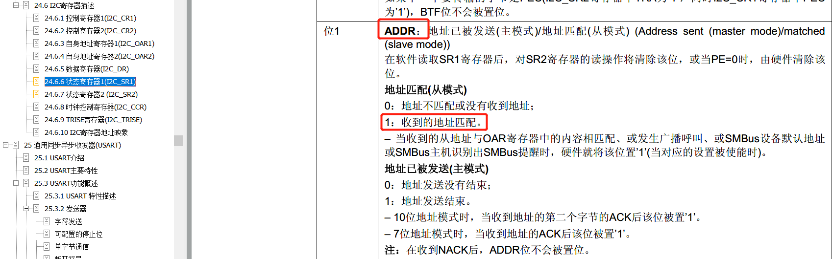
Generate the device address and wait for the response signal. If there is a slave response, the time EV6 and EV8 will be generated. At this time, the ADDR bit and TXE bit of SR1 register are set to 1 (as shown in the figure below). ADDR bit 1 indicates that the address has been sent, and TEX indicates that the data register is empty.
-
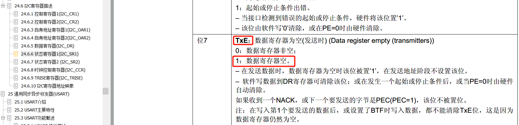
Write the data to be sent to the IIC data register DR. at this time, the TXE bit will be reset to 0, indicating that the data register is not empty. After the IIC peripheral sends the data through one bit of the SDA signal line, an EV8 event will be generated, that is, the TXE is set to 1. Repeat this process to send multiple bytes.
-
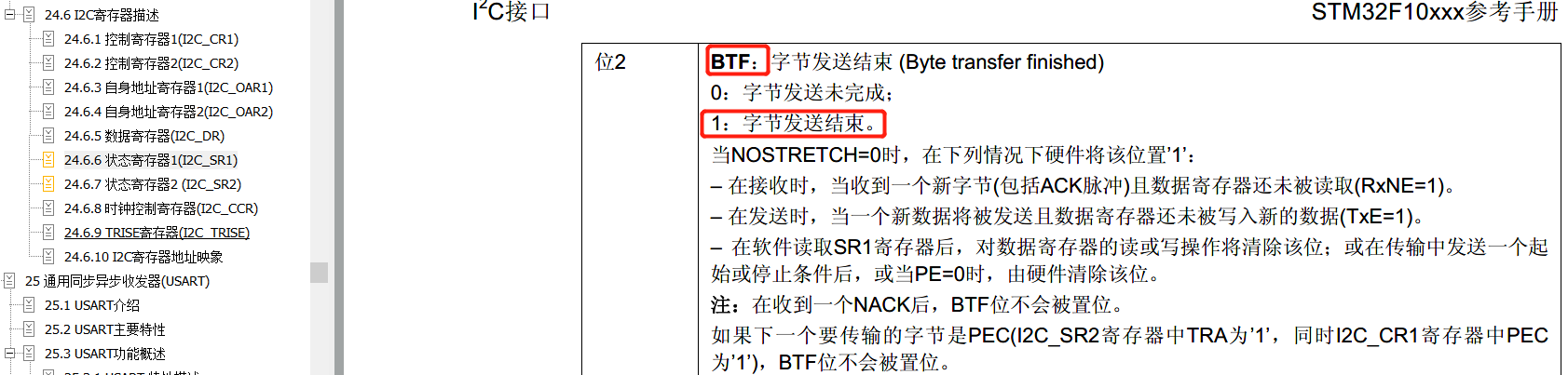
After sending data, control IIC equipment to generate a stop signal P. at this time, EV2 event is generated. TEX bit and BTF bit of SR1 are set to 1 (as shown in the figure below), indicating the end of communication.
IIC structure and library function of STM32
IIC structure of STM32
In firmware package I2C H inside
typedef struct
{
  uint32_t I2C_ClockSpeed;     //Set the SCL clock frequency, which should be lower than 400 000
  uint16_t I2C_Mode;           //Specify the working mode and select IIC mode and SMBUS mode
  uint16_t I2C_DutyCycle;      //Clock duty cycle, optional low/high = 2:0 or 16:9
  uint16_t I2C_OwnAddress1;  //Own IIC device address
  uint16_t I2C_Ack;           //Enable or close the response, usually enable
  uint16_t I2C_AcknowledgedAddress; //Specify the address length, which can be 7 or 10
}I2C_InitTypeDef;
-
I2C_ClockSpeed
Set the transmission rate of IIC. When calling the initialization function, the function will write the clock factor into the clock control register CCR of IIC after operation according to the value we input. The parameter value we write should not be higher than 400Khz (as shown in the figure below).
In fact, because the CCR register cannot write the clock factor of decimal type, the actual frequency affecting SCL may be lower than the parameter value set by this member. At this time, except that the communication will be a little slower, it will not have any other impact on the standard communication of IIC.
-
I2C_Mode
Select IIC mode (IIC_Mode_IIC) and SMBus master and slave modes (IIC_Mode_SMBusHost, IIC_Mode_SMBusDevice)
IIC does not need to distinguish the master-slave mode here. Set IIC directly_ Mode_ Iicj is enough -
I2C_DutyCycle
Set the duty cycle of SCL line clock of IIC. There are two options for this configuration: the low-level time is 2:1(IIC_DutyCycle_2) and the high-level time is 16:9 (IIC_DutyCycle_16_9)
In fact, the proportion difference between the two modes is not big, and the general requirements will not be so strict. Just choose it here.
-
I2C_OwnAddress1
Configure the IIC device of STM32 with its own address. Each device connected to the IIC bus has its own address, and the host is no exception. The address can be set to 7 or 10 bits (determined by the iic_knowledgeaddress member below), as long as the address is unique on the IIC bus.
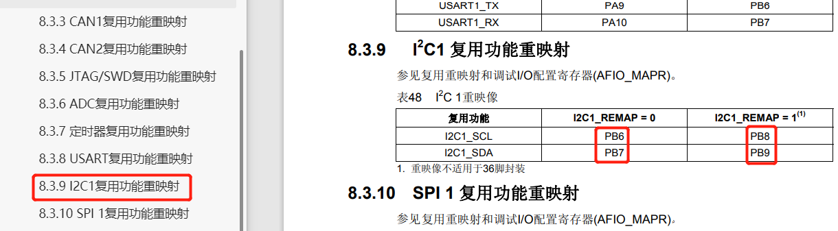
The IIC peripheral of STM32 can use two addresses at the same time (as shown in the figure below), that is, respond to two addresses at the same time (very flexible). This structure member IIC_OwnAddress1 is configured as the default address stored in the OAR1 register. If you need to set the second address register OAR2, you can use IIC_ Owmaddress 2conig function to configure. OAR2 does not support 10 bit addresses.
-
I2C_Ack
Configure whether the IIC response is enabled. If the bit is enabled, the response signal can be sent. Generally, the configuration bit allows the response (IIC_Ack_Enable), which is the communication requirement of most devices that follow the IIC standard. Changing to IIC_Ack_Disable will often lead to communication errors. -
I2C_AcknowledgedAddress
The addressing mode of IIC is 7-bit or 10 bit address, which needs to be selected according to the address of the device actually connected to the IIC bus. The configuration of this member also affects the IIC_OwnAddress member, IIC only when it is set to 10 bit mode here_ Ownaddress1 only supports 10 bit addresses
After configuring the values of these structure members, call the library function IIC_Init can write the configuration of the structure into the corresponding register.
IIC library function of STM32
Firmware package h documents are given, only some are listed.
//Configure own device address 2
void I2C_OwnAddress2Config(I2C_TypeDef* I2Cx, uint8_t Address);

//Sending device address
void I2C_Send7bitAddress(I2C_TypeDef* I2Cx, uint8_t Address, uint8_t I2C_Direction);

//receive data
uint8_t I2C_ReceiveData(I2C_TypeDef* I2Cx);

//Stop receiving
void I2C_AcknowledgeConfig(I2C_TypeDef* I2Cx, FunctionalState NewState);

 //IIC peripherals begin to work normally
void I2C_Cmd(I2C_TypeDef* I2Cx, FunctionalState NewState);
OLED screen introduction
OLED is organic light emitting diode (OLED). OLED display technology has some advantages, such as self luminescence, wide viewing angle, almost infinite high contrast, low power consumption, very high reaction speed, can be used for curved panels, wide temperature range, simple structure and process, etc. it is considered to be a new application technology of the next generation of flat display screen.
OLED display is different from traditional LCD display. It can emit light by itself, so there is no need for backlight, which makes OLED display thinner than LCD display and better display effect.
Commonly used OLED screens are blue, yellow, white and so on. The size of the screen is 0.96 inches and the pixel points are
128 * 64, so we call it 0.96 OLED screen or 12864 screen.
OLED screen features
1. Module size: 23.7 *23.8mm
2. Power supply voltage: 3.3-5.5V
3. Driver chip: SSD1306
4. Test platform: provide k60/k10,9s12XS128,51,stm32, stm8 and other MCU
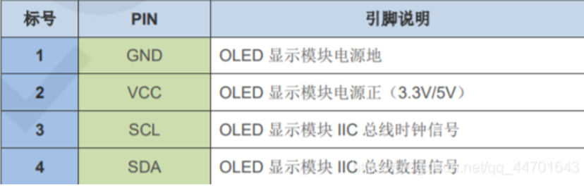
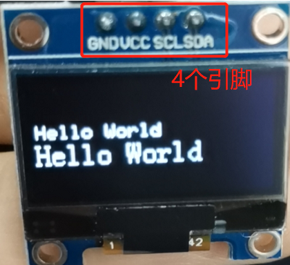
OLED screen wiring instructions
OLED screen memory
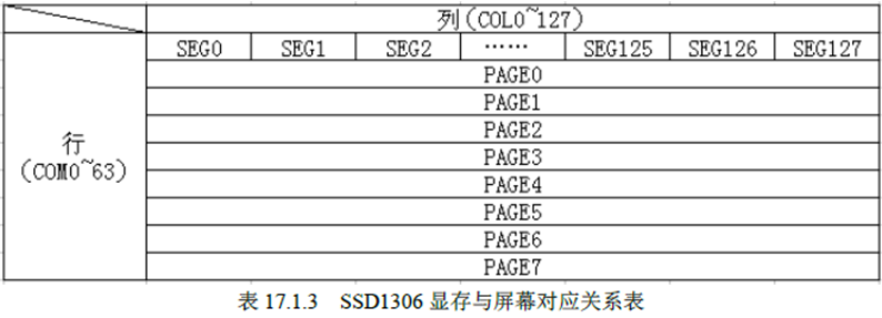
OLED itself has no video memory. Its video memory depends on SSD1306 (driver chip), which provides a piece of video memory.
The SSD1306 video memory has a total size of 128*64bit. SSD1306 divides these video memories into 8 pages. Each page contains 128 bytes.
OLED screen principle
A cache (128 * 8 bytes in total) is built in STM32. Each time it is modified, only the cache on STM32 (actually SRAM) is modified. After modification, the cache data on STM32 is written to OLED GRAM at one time.
This method also has disadvantages. It is troublesome for a very small single chip microcomputer (51 Series) of SRAM.
Common instructions for OLED screen
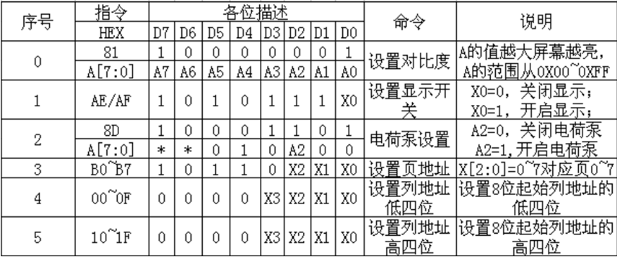
The second column in the figure above: use of instructions
- Instruction 0X81: set contrast. It contains two bytes. The first 0X81 is the command, and then the method is to set the contrast. The larger the value, the brighter the screen.
- Instruction 0XAE/0XAF: 0XAE is the command to turn off display, and 0XAF is the command to turn on display
- Instruction 0X8D: contains two bytes. The first is the command word, the second is the setting value, and BIT2 in the second byte indicates the switching state of the charge pump. This bit is 1 to start the charge pump, and 0 to close it. When the module is initialized, this must be turned on, otherwise the screen display cannot be seen.
- Instructions 0XB0~B7: used to set the page address (as mentioned earlier, it is divided into 8 pages in total), and the value of the lower three bits corresponds to the GRAM page address (it is well understood that binary three bits can represent 0 – 8).
- Instruction 0X00~0X0F: used to set the lower four digits of the starting column address during display.
- Instructions 0X10~0X1F: used to set the upper four digits of the starting column address during display.
Use of OLED screen font software
OLED dot mode (64 * 128 dot matrix)
The lighting mode of OLED dot matrix, for example, shows "P", the leftmost bit and the highest bit P7.
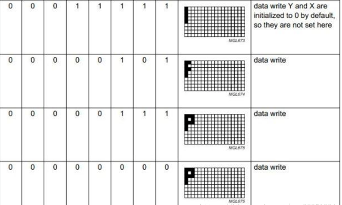
The numbers on the left are written from bottom to top in the dot matrix on the right
-
1. It can be seen that if you want to display "P", first write 0x1f, a vertical bar will be displayed, and then the controller will automatically move horizontally to the next column.
-
2. If 0X05 is written again, two small cross bars will appear, which are the positions of two 1 in 0000 0101 in 0X05. After writing the second column, the controller will automatically jump to the third column
-
3. After writing 0X07 and 0X00 in the fourth column, P will be displayed. This also shows that even if you only want to display a small dot at the top of the column, that is, write 0X01
-
4. One dot matrix cannot be controlled at one time, only eight bit dot matrix can be controlled at one time, that is, one column of dot matrix. This also determines that the mode of font selection is "column type".
OLED display string
Display effect:
oled.c
#include "stm32f10x.h"
#include "oled.h"
#include "delay.h"
#include "OLED_Codetab.h" / / font is given below


//The OLED storage format is divided into 8 pages, each of which is 8 * 128 (as shown below)
//[0]0 1 2 3 ... 127
//[1]0 1 2 3 ... 127
//[2]0 1 2 3 ... 127
//[3]0 1 2 3 ... 127
//[4]0 1 2 3 ... 127
//[5]0 1 2 3 ... 127
//[6]0 1 2 3 ... 127
//[7]0 1 2 3 ... 127


void I2C_Configuration(void)
{
	I2C_InitTypeDef   I2C_InitStructure;   //I2C structure configuration H inside
	GPIO_InitTypeDef  GPIO_InitStructure;  //GPIO structure configuration
    RCC_APB2PeriphClockCmd(RCC_APB2Periph_GPIOB, ENABLE); //Clock enable RCC H inside
    RCC_APB1PeriphClockCmd(RCC_APB1Periph_I2C1, ENABLE);

	//PB6 - > SCL pb7 - > SDA wiring mode
	GPIO_InitStructure.GPIO_Mode   =  GPIO_Mode_AF_OD;//IIC select multiplex open drain
	GPIO_InitStructure.GPIO_Pin    =  GPIO_Pin_7 | GPIO_Pin_6;
	GPIO_InitStructure.GPIO_Speed  =  GPIO_Speed_50MHz;
    GPIO_Init(GPIOB,&GPIO_InitStructure);


	//I2C
    I2C_DeInit(I2C1);//Initialize using it
	I2C_InitStructure.I2C_Ack                   =  I2C_Ack_Enable;//Reply enable
	I2C_InitStructure.I2C_AcknowledgedAddress   =  I2C_AcknowledgedAddress_7bit;//Select 7 bits for the address
	I2C_InitStructure.I2C_ClockSpeed            =  400000;//Clock speed 400K
	I2C_InitStructure.I2C_DutyCycle             =  I2C_DutyCycle_2;//2: 1:16:9 is OK
	I2C_InitStructure.I2C_Mode                  =  I2C_Mode_I2C;//I2C mode
	I2C_InitStructure.I2C_OwnAddress1           =  0X10;//Write the host address casually
    I2C_Init( I2C1, &I2C_InitStructure);//initialization
    I2C_Cmd( I2C1,  ENABLE); //Enable I2C1

}


//Hardware IIC configuration
//Compare with the above: IIC feature and architecture of STM32 3 Data control logic diagram
void I2C_WriteByte(uint8_t addr , uint8_t data)
{
	while(I2C_GetFlagStatus(I2C1,  I2C_FLAG_BUSY));  //Check whether the I2C bus is busy and wait for the busy end
    I2C_GenerateSTART(I2C1,  ENABLE);               //Open IIC1
    while(!I2C_CheckEvent(I2C1,  I2C_EVENT_MASTER_MODE_SELECT)); //EV5 main mode check whether to answer
    I2C_Send7bitAddress(I2C1, OLED_ADDRESS,  I2C_Direction_Transmitter);  //Generator address (7 bits) OLED_ The value of address is in OLED H defines the direction: send broadcast status (find the slave address)
	while(!I2C_CheckEvent(I2C1 ,I2C_EVENT_MASTER_RECEIVER_MODE_SELECTED));  //EV6

    I2C_SendData( I2C1,  addr); //Send register address parameter
	while(!I2C_CheckEvent(I2C1,  I2C_EVENT_MASTER_BYTE_TRANSMITTING)); //EV8 main mode needs a response every time it is sent. It needs to detect the response
    I2C_SendData( I2C1 , data);  //Send data parameters
	while(!I2C_CheckEvent(I2C1,  I2C_EVENT_MASTER_BYTE_TRANSMITTING)); //EV8 Ö÷ģʽ

    I2C_GenerateSTOP(I2C1,ENABLE  );  //Turn off I2C bus

}


//To OLED
//Write command
void WriteCmd(unsigned char I2C_Cmd)
{
	I2C_WriteByte(0X00,I2C_Cmd);//The firmware library function is written in the 0X00 address (ROM)
}


//Write data
void  WriteData(unsigned char I2C_Data)
{
	I2C_WriteByte(0X40 , I2C_Data);
}


//OELD screen initialization
void OLED_Init(void)
{
   //below 	 This part of the code is provided by the manufacturer and copied
    delay_ms(100);
	WriteCmd(0xAE); //display off
	WriteCmd(0x20);	//Set Memory Addressing Mode
	WriteCmd(0x10);	//00,Horizontal Addressing Mode;01,Vertical Addressing Mode;10,Page Addressing Mode (RESET);11,Invalid
	WriteCmd(0xb0);	//Set Page Start Address for Page Addressing Mode,0-7
	WriteCmd(0xc8);	//Set COM Output Scan Direction
	WriteCmd(0x00); //---set low column address
	WriteCmd(0x10); //---set high column address
	WriteCmd(0x40); //--set start line address
	WriteCmd(0x81); //--set contrast control register
	WriteCmd(0xff); //ÁÁ¶Èµ÷½Ú 0x00~0xff
	WriteCmd(0xa1); //--set segment re-map 0 to 127
	WriteCmd(0xa6); //--set normal display
	WriteCmd(0xa8); //--set multiplex ratio(1 to 64)
	WriteCmd(0x3F); //
	WriteCmd(0xa4); //0xa4,Output follows RAM content;0xa5,Output ignores RAM content
	WriteCmd(0xd3); //-set display offset
	WriteCmd(0x00); //-not offset
	WriteCmd(0xd5); //--set display clock divide ratio/oscillator frequency
	WriteCmd(0xf0); //--set divide ratio
	WriteCmd(0xd9); //--set pre-charge period
	WriteCmd(0x22); //
	WriteCmd(0xda); //--set com pins hardware configuration
	WriteCmd(0x12);
	WriteCmd(0xdb); //--set vcomh
	WriteCmd(0x20); //0x20,0.77xVcc
	WriteCmd(0x8d); //--set DC-DC enable
	WriteCmd(0x14); //
	WriteCmd(0xaf); //--turn on oled panel
}


//Set start coordinates
void OLED_SetPos(unsigned char x, unsigned char y)
{
	WriteCmd(0xb0 + y);    //These are fixed, but also look at the instruction table above
	WriteCmd((x & 0xf0) >> 4 | 0x10); //Take high position
	WriteCmd((x & 0x0f ) | 0x01);     //Take low position
}


//Full screen fill black dot
void OLED_Full(unsigned char Full_Data)
{
	unsigned char n, m ;//As mentioned earlier, the screen is divided into 8 pages, each of which needs to be processed
	for( m = 0 ; m < 8 ; m++)
		{
			WriteCmd(0xb0 + m);//0xb0 is above the starting point coordinate of column
			WriteCmd(0x00);
			WriteCmd(0x10);

			for( n = 0 ; n < 128 ; n++)//128 columns
			{
				WriteData(Full_Data);
			}
		}
}


//The screen clearing function makes the screen display nothing
void OLED_Clear(void)
{
	OLED_Full(0x00);
}


//oled turns on the pump
void OLED_Open(void)
{
	WriteCmd(0x8D); //Set charge pump command (available on the command table)
	WriteCmd(0x14);  //Turn on the charge pump
	WriteCmd(0xaf);  //The case of OLED wake-up instruction can be consistent with the instruction table

}


//oled off
void OLED_Close(void)
{
	WriteCmd(0x8D);
	WriteCmd(0x10);  //Turn off the charge pump
	WriteCmd(0xAE);  //Turn off oled
}


//Display string coordinates 								 The content format to be displayed is 6 * 8 * 16
void OLED_ShowStr(unsigned char x, unsigned char y , unsigned char ch[] , unsigned TestSize)
{
	unsigned char c = 0 , i = 0, j = 0;
	switch(TestSize)
	{
		case 1://6*8
		{
			while(ch[j] != '\0')//String end tag
			{
				c = ch[j] - 32;//Case conversion
				if(x > 126)//X is out of bounds. Put it in the first position
				{
					x = 0 ;
					y ++;
				}
				OLED_SetPos(x , y);
				for( i = 0 ; i< 6 ; i++)
					WriteData(F6X8[c][i]);//Displayed on the screen, F6X8 is in the header file
					x+= 6;//Format: 6 * 8 jump to the next character (6 characters in the header file)
					j++;
			}
		}break;

		case 2://8*16
		{
				while(ch[j] != '\0'){
					c = ch[j] - 32;
					if( x > 120)
					{
						x = 0;
						y++;
					}
					OLED_SetPos(x , y);
					for( i = 0 ; i < 8 ; i++)//The 16 is divided into two parts, and the screen is divided into 8 pages to display up and down (not quite understood at present)
					WriteData(F8X16[c*16 + i]);
					OLED_SetPos(x , y+1);
					for( i = 0 ; i < 8 ; i++)
					WriteData(F8X16[c*16+i+8]);
					x+=8;//Go to next character
					j++;
				}
			}break;
	}
}


//display text
void OLED_ShowCn(unsigned char x, unsigned char y , unsigned char N)
{
	unsigned char wn = 0;
	unsigned  int addr = 32*N;//A word is represented by 32 hexadecimals
	OLED_SetPos(x , y);

	for( wn = 0 ; wn < 16 ; wn++)//A word is represented by 32 hexadecimals and is divided into two parts
	{
		WriteData(F16X16[addr]);
		addr+= 1;
	}
	OLED_SetPos(x , y+1);//y+1 on the next page
	for( wn = 0 ; wn < 16 ; wn++)
	{
		WriteData(F16X16[addr]);
		addr+= 1;
	}

}


//Displays the start and end diagonals of the image
void OLED_ShowBMP(unsigned char x0 , unsigned char y0 , unsigned char x1 , unsigned char y1 , unsigned char BMP[])
{
	unsigned int j = 0;
	unsigned char x , y;
	if(y1 % 8 == 0)
	{
		y = y1/8;
	}
	else
	{
		y = y1/8 +1;
	}
	for(y = y0 ; y< y1 ; y++)//y is equivalent to the number of pages. Each page has 8 lines
	{
		OLED_SetPos(x0 ,y);
		for( x= x0 ; x < x1 ; x++)
		{
			WriteData(BMP[j++]);
		}
	}
}
oled.h
#ifndef _OLED_H_
#define _OLED_H_// Conditional compilation performs the following operations

#include "stm32f10x.h"
#define  OLED_ADDRESS 0x78 / / definition without semicolon!!
void I2C_Configuration(void);
void I2C_WriteByte(uint8_t addr , uint8_t data);
void WriteCmd(unsigned char I2C_Cmd);
void WriteData(unsigned char I2C_Data);
void OLED_Init(void);
void OLED_SetPos(unsigned char x, unsigned char y);
void OLED_Full(unsigned char Full_Data);
void OLED_Clear(void);
void OLED_Open(void);
void OLED_Close(void);
void OLED_ShowStr(unsigned char x, unsigned char y , unsigned char ch[] , unsigned TestSize);
void OLED_ShowCn(unsigned char x, unsigned char y , unsigned char N);

#endif
OLED_Codetab.h
//Character header file
const unsigned char F16X16[] =
{
	0x00,0x00,0x00,0xE0,0x00,0x00,0x00,0xFF,0x00,0x00,0x00,0x20,0x40,0x80,0x00,0x00,
	0x08,0x04,0x03,0x00,0x00,0x40,0x80,0x7F,0x00,0x00,0x00,0x00,0x00,0x01,0x0E,0x00,Small",0*/
	0x00,0x00,0xFE,0xAA,0xAA,0xA9,0xF9,0x00,0xA0,0x9E,0x82,0x82,0x9E,0xA0,0x20,0x00,
	0x40,0x30,0x0F,0x02,0x22,0x42,0x3E,0x80,0x80,0x43,0x2C,0x10,0x2C,0x43,0x80,0x00,/*Yin ", 1*/
	0x00,0x00,0xFE,0x02,0x12,0x92,0x92,0x92,0x92,0x92,0x92,0x12,0x02,0xFE,0x00,0x00,
	0x00,0x00,0xFF,0x00,0x00,0x1F,0x08,0x08,0x08,0x08,0x1F,0x40,0x80,0x7F,0x00,0x00,/*"Same as ", 2*/
	0x40,0x30,0x11,0x96,0x90,0x90,0x91,0x96,0x90,0x90,0x98,0x14,0x13,0x50,0x30,0x00,
	0x04,0x04,0x04,0x04,0x04,0x44,0x84,0x7E,0x06,0x05,0x04,0x04,0x04,0x04,0x04,0x00,/*""Learning", 3*/

};

//The above Chinese character code is generated according to the font software


//Continue placing image fonts


const unsigned char F6X8[][6] =
{
	0x00, 0x00, 0x00, 0x00, 0x00, 0x00,// sp
	0x00, 0x00, 0x00, 0x2f, 0x00, 0x00,// !
	0x00, 0x00, 0x07, 0x00, 0x07, 0x00,// "
	0x00, 0x14, 0x7f, 0x14, 0x7f, 0x14,// #
	0x00, 0x24, 0x2a, 0x7f, 0x2a, 0x12,// $
	0x00, 0x62, 0x64, 0x08, 0x13, 0x23,// %
	0x00, 0x36, 0x49, 0x55, 0x22, 0x50,// &
	0x00, 0x00, 0x05, 0x03, 0x00, 0x00,// '
	0x00, 0x00, 0x1c, 0x22, 0x41, 0x00,// (
	0x00, 0x00, 0x41, 0x22, 0x1c, 0x00,// )
	0x00, 0x14, 0x08, 0x3E, 0x08, 0x14,// *
	0x00, 0x08, 0x08, 0x3E, 0x08, 0x08,// +
	0x00, 0x00, 0x00, 0xA0, 0x60, 0x00,// ,
	0x00, 0x08, 0x08, 0x08, 0x08, 0x08,// -
	0x00, 0x00, 0x60, 0x60, 0x00, 0x00,// .
	0x00, 0x20, 0x10, 0x08, 0x04, 0x02,// /
	0x00, 0x3E, 0x51, 0x49, 0x45, 0x3E,// 0
	0x00, 0x00, 0x42, 0x7F, 0x40, 0x00,// 1
	0x00, 0x42, 0x61, 0x51, 0x49, 0x46,// 2
	0x00, 0x21, 0x41, 0x45, 0x4B, 0x31,// 3
	0x00, 0x18, 0x14, 0x12, 0x7F, 0x10,// 4
	0x00, 0x27, 0x45, 0x45, 0x45, 0x39,// 5
	0x00, 0x3C, 0x4A, 0x49, 0x49, 0x30,// 6
	0x00, 0x01, 0x71, 0x09, 0x05, 0x03,// 7
	0x00, 0x36, 0x49, 0x49, 0x49, 0x36,// 8
	0x00, 0x06, 0x49, 0x49, 0x29, 0x1E,// 9
	0x00, 0x00, 0x36, 0x36, 0x00, 0x00,// :
	0x00, 0x00, 0x56, 0x36, 0x00, 0x00,// ;
	0x00, 0x08, 0x14, 0x22, 0x41, 0x00,// <
	0x00, 0x14, 0x14, 0x14, 0x14, 0x14,// =
	0x00, 0x00, 0x41, 0x22, 0x14, 0x08,// >
	0x00, 0x02, 0x01, 0x51, 0x09, 0x06,// ?
	0x00, 0x32, 0x49, 0x59, 0x51, 0x3E,// @
	0x00, 0x7C, 0x12, 0x11, 0x12, 0x7C,// A
	0x00, 0x7F, 0x49, 0x49, 0x49, 0x36,// B
	0x00, 0x3E, 0x41, 0x41, 0x41, 0x22,// C
	0x00, 0x7F, 0x41, 0x41, 0x22, 0x1C,// D
	0x00, 0x7F, 0x49, 0x49, 0x49, 0x41,// E
	0x00, 0x7F, 0x09, 0x09, 0x09, 0x01,// F
	0x00, 0x3E, 0x41, 0x49, 0x49, 0x7A,// G
	0x00, 0x7F, 0x08, 0x08, 0x08, 0x7F,// H
	0x00, 0x00, 0x41, 0x7F, 0x41, 0x00,// I
	0x00, 0x20, 0x40, 0x41, 0x3F, 0x01,// J
	0x00, 0x7F, 0x08, 0x14, 0x22, 0x41,// K
	0x00, 0x7F, 0x40, 0x40, 0x40, 0x40,// L
	0x00, 0x7F, 0x02, 0x0C, 0x02, 0x7F,// M
	0x00, 0x7F, 0x04, 0x08, 0x10, 0x7F,// N
	0x00, 0x3E, 0x41, 0x41, 0x41, 0x3E,// O
	0x00, 0x7F, 0x09, 0x09, 0x09, 0x06,// P
	0x00, 0x3E, 0x41, 0x51, 0x21, 0x5E,// Q
	0x00, 0x7F, 0x09, 0x19, 0x29, 0x46,// R
	0x00, 0x46, 0x49, 0x49, 0x49, 0x31,// S
	0x00, 0x01, 0x01, 0x7F, 0x01, 0x01,// T
	0x00, 0x3F, 0x40, 0x40, 0x40, 0x3F,// U
	0x00, 0x1F, 0x20, 0x40, 0x20, 0x1F,// V
	0x00, 0x3F, 0x40, 0x38, 0x40, 0x3F,// W
	0x00, 0x63, 0x14, 0x08, 0x14, 0x63,// X
	0x00, 0x07, 0x08, 0x70, 0x08, 0x07,// Y
	0x00, 0x61, 0x51, 0x49, 0x45, 0x43,// Z
	0x00, 0x00, 0x7F, 0x41, 0x41, 0x00,// [
	0x00, 0x55, 0x2A, 0x55, 0x2A, 0x55,// 55
	0x00, 0x00, 0x41, 0x41, 0x7F, 0x00,// ]
	0x00, 0x04, 0x02, 0x01, 0x02, 0x04,// ^
	0x00, 0x40, 0x40, 0x40, 0x40, 0x40,// _
	0x00, 0x00, 0x01, 0x02, 0x04, 0x00,// '
	0x00, 0x20, 0x54, 0x54, 0x54, 0x78,// a
	0x00, 0x7F, 0x48, 0x44, 0x44, 0x38,// b
	0x00, 0x38, 0x44, 0x44, 0x44, 0x20,// c
	0x00, 0x38, 0x44, 0x44, 0x48, 0x7F,// d
	0x00, 0x38, 0x54, 0x54, 0x54, 0x18,// e
	0x00, 0x08, 0x7E, 0x09, 0x01, 0x02,// f
	0x00, 0x18, 0xA4, 0xA4, 0xA4, 0x7C,// g
	0x00, 0x7F, 0x08, 0x04, 0x04, 0x78,// h
	0x00, 0x00, 0x44, 0x7D, 0x40, 0x00,// i
	0x00, 0x40, 0x80, 0x84, 0x7D, 0x00,// j
	0x00, 0x7F, 0x10, 0x28, 0x44, 0x00,// k
	0x00, 0x00, 0x41, 0x7F, 0x40, 0x00,// l
	0x00, 0x7C, 0x04, 0x18, 0x04, 0x78,// m
	0x00, 0x7C, 0x08, 0x04, 0x04, 0x78,// n
	0x00, 0x38, 0x44, 0x44, 0x44, 0x38,// o
	0x00, 0xFC, 0x24, 0x24, 0x24, 0x18,// p
	0x00, 0x18, 0x24, 0x24, 0x18, 0xFC,// q
	0x00, 0x7C, 0x08, 0x04, 0x04, 0x08,// r
	0x00, 0x48, 0x54, 0x54, 0x54, 0x20,// s
	0x00, 0x04, 0x3F, 0x44, 0x40, 0x20,// t
	0x00, 0x3C, 0x40, 0x40, 0x20, 0x7C,// u
	0x00, 0x1C, 0x20, 0x40, 0x20, 0x1C,// v
	0x00, 0x3C, 0x40, 0x30, 0x40, 0x3C,// w
	0x00, 0x44, 0x28, 0x10, 0x28, 0x44,// x
	0x00, 0x1C, 0xA0, 0xA0, 0xA0, 0x7C,// y
	0x00, 0x44, 0x64, 0x54, 0x4C, 0x44,// z
	0x14, 0x14, 0x14, 0x14, 0x14, 0x14,// horiz lines
};
const unsigned char F8X16[]=
{
  0x00,0x00,0x00,0x00,0x00,0x00,0x00,0x00,0x00,0x00,0x00,0x00,0x00,0x00,0x00,0x00,// 0
  0x00,0x00,0x00,0xF8,0x00,0x00,0x00,0x00,0x00,0x00,0x00,0x33,0x30,0x00,0x00,0x00,//! 1
  0x00,0x10,0x0C,0x06,0x10,0x0C,0x06,0x00,0x00,0x00,0x00,0x00,0x00,0x00,0x00,0x00,//" 2
  0x40,0xC0,0x78,0x40,0xC0,0x78,0x40,0x00,0x04,0x3F,0x04,0x04,0x3F,0x04,0x04,0x00,//# 3
  0x00,0x70,0x88,0xFC,0x08,0x30,0x00,0x00,0x00,0x18,0x20,0xFF,0x21,0x1E,0x00,0x00,//$ 4
  0xF0,0x08,0xF0,0x00,0xE0,0x18,0x00,0x00,0x00,0x21,0x1C,0x03,0x1E,0x21,0x1E,0x00,//% 5
  0x00,0xF0,0x08,0x88,0x70,0x00,0x00,0x00,0x1E,0x21,0x23,0x24,0x19,0x27,0x21,0x10,//& 6
  0x10,0x16,0x0E,0x00,0x00,0x00,0x00,0x00,0x00,0x00,0x00,0x00,0x00,0x00,0x00,0x00,//' 7
  0x00,0x00,0x00,0xE0,0x18,0x04,0x02,0x00,0x00,0x00,0x00,0x07,0x18,0x20,0x40,0x00,//( 8
  0x00,0x02,0x04,0x18,0xE0,0x00,0x00,0x00,0x00,0x40,0x20,0x18,0x07,0x00,0x00,0x00,//) 9
  0x40,0x40,0x80,0xF0,0x80,0x40,0x40,0x00,0x02,0x02,0x01,0x0F,0x01,0x02,0x02,0x00,//* 10
  0x00,0x00,0x00,0xF0,0x00,0x00,0x00,0x00,0x01,0x01,0x01,0x1F,0x01,0x01,0x01,0x00,//+ 11
  0x00,0x00,0x00,0x00,0x00,0x00,0x00,0x00,0x80,0xB0,0x70,0x00,0x00,0x00,0x00,0x00,//, 12
  0x00,0x00,0x00,0x00,0x00,0x00,0x00,0x00,0x00,0x01,0x01,0x01,0x01,0x01,0x01,0x01,//- 13
  0x00,0x00,0x00,0x00,0x00,0x00,0x00,0x00,0x00,0x30,0x30,0x00,0x00,0x00,0x00,0x00,//. 14
  0x00,0x00,0x00,0x00,0x80,0x60,0x18,0x04,0x00,0x60,0x18,0x06,0x01,0x00,0x00,0x00,/// 15
  0x00,0xE0,0x10,0x08,0x08,0x10,0xE0,0x00,0x00,0x0F,0x10,0x20,0x20,0x10,0x0F,0x00,//0 16
  0x00,0x10,0x10,0xF8,0x00,0x00,0x00,0x00,0x00,0x20,0x20,0x3F,0x20,0x20,0x00,0x00,//1 17
  0x00,0x70,0x08,0x08,0x08,0x88,0x70,0x00,0x00,0x30,0x28,0x24,0x22,0x21,0x30,0x00,//2 18
  0x00,0x30,0x08,0x88,0x88,0x48,0x30,0x00,0x00,0x18,0x20,0x20,0x20,0x11,0x0E,0x00,//3 19
  0x00,0x00,0xC0,0x20,0x10,0xF8,0x00,0x00,0x00,0x07,0x04,0x24,0x24,0x3F,0x24,0x00,//4 20
  0x00,0xF8,0x08,0x88,0x88,0x08,0x08,0x00,0x00,0x19,0x21,0x20,0x20,0x11,0x0E,0x00,//5 21
  0x00,0xE0,0x10,0x88,0x88,0x18,0x00,0x00,0x00,0x0F,0x11,0x20,0x20,0x11,0x0E,0x00,//6 22
  0x00,0x38,0x08,0x08,0xC8,0x38,0x08,0x00,0x00,0x00,0x00,0x3F,0x00,0x00,0x00,0x00,//7 23
  0x00,0x70,0x88,0x08,0x08,0x88,0x70,0x00,0x00,0x1C,0x22,0x21,0x21,0x22,0x1C,0x00,//8 24
  0x00,0xE0,0x10,0x08,0x08,0x10,0xE0,0x00,0x00,0x00,0x31,0x22,0x22,0x11,0x0F,0x00,//9 25
  0x00,0x00,0x00,0xC0,0xC0,0x00,0x00,0x00,0x00,0x00,0x00,0x30,0x30,0x00,0x00,0x00,//: 26
  0x00,0x00,0x00,0x80,0x00,0x00,0x00,0x00,0x00,0x00,0x80,0x60,0x00,0x00,0x00,0x00,//; 27
  0x00,0x00,0x80,0x40,0x20,0x10,0x08,0x00,0x00,0x01,0x02,0x04,0x08,0x10,0x20,0x00,//< 28
  0x40,0x40,0x40,0x40,0x40,0x40,0x40,0x00,0x04,0x04,0x04,0x04,0x04,0x04,0x04,0x00,//= 29
  0x00,0x08,0x10,0x20,0x40,0x80,0x00,0x00,0x00,0x20,0x10,0x08,0x04,0x02,0x01,0x00,//> 30
  0x00,0x70,0x48,0x08,0x08,0x08,0xF0,0x00,0x00,0x00,0x00,0x30,0x36,0x01,0x00,0x00,//? 31
  0xC0,0x30,0xC8,0x28,0xE8,0x10,0xE0,0x00,0x07,0x18,0x27,0x24,0x23,0x14,0x0B,0x00,//@ 32
  0x00,0x00,0xC0,0x38,0xE0,0x00,0x00,0x00,0x20,0x3C,0x23,0x02,0x02,0x27,0x38,0x20,//A 33
  0x08,0xF8,0x88,0x88,0x88,0x70,0x00,0x00,0x20,0x3F,0x20,0x20,0x20,0x11,0x0E,0x00,//B 34
  0xC0,0x30,0x08,0x08,0x08,0x08,0x38,0x00,0x07,0x18,0x20,0x20,0x20,0x10,0x08,0x00,//C 35
  0x08,0xF8,0x08,0x08,0x08,0x10,0xE0,0x00,0x20,0x3F,0x20,0x20,0x20,0x10,0x0F,0x00,//D 36
  0x08,0xF8,0x88,0x88,0xE8,0x08,0x10,0x00,0x20,0x3F,0x20,0x20,0x23,0x20,0x18,0x00,//E 37
  0x08,0xF8,0x88,0x88,0xE8,0x08,0x10,0x00,0x20,0x3F,0x20,0x00,0x03,0x00,0x00,0x00,//F 38
  0xC0,0x30,0x08,0x08,0x08,0x38,0x00,0x00,0x07,0x18,0x20,0x20,0x22,0x1E,0x02,0x00,//G 39
  0x08,0xF8,0x08,0x00,0x00,0x08,0xF8,0x08,0x20,0x3F,0x21,0x01,0x01,0x21,0x3F,0x20,//H 40
  0x00,0x08,0x08,0xF8,0x08,0x08,0x00,0x00,0x00,0x20,0x20,0x3F,0x20,0x20,0x00,0x00,//I 41
  0x00,0x00,0x08,0x08,0xF8,0x08,0x08,0x00,0xC0,0x80,0x80,0x80,0x7F,0x00,0x00,0x00,//J 42
  0x08,0xF8,0x88,0xC0,0x28,0x18,0x08,0x00,0x20,0x3F,0x20,0x01,0x26,0x38,0x20,0x00,//K 43
  0x08,0xF8,0x08,0x00,0x00,0x00,0x00,0x00,0x20,0x3F,0x20,0x20,0x20,0x20,0x30,0x00,//L 44
  0x08,0xF8,0xF8,0x00,0xF8,0xF8,0x08,0x00,0x20,0x3F,0x00,0x3F,0x00,0x3F,0x20,0x00,//M 45
  0x08,0xF8,0x30,0xC0,0x00,0x08,0xF8,0x08,0x20,0x3F,0x20,0x00,0x07,0x18,0x3F,0x00,//N 46
  0xE0,0x10,0x08,0x08,0x08,0x10,0xE0,0x00,0x0F,0x10,0x20,0x20,0x20,0x10,0x0F,0x00,//O 47
  0x08,0xF8,0x08,0x08,0x08,0x08,0xF0,0x00,0x20,0x3F,0x21,0x01,0x01,0x01,0x00,0x00,//P 48
  0xE0,0x10,0x08,0x08,0x08,0x10,0xE0,0x00,0x0F,0x18,0x24,0x24,0x38,0x50,0x4F,0x00,//Q 49
  0x08,0xF8,0x88,0x88,0x88,0x88,0x70,0x00,0x20,0x3F,0x20,0x00,0x03,0x0C,0x30,0x20,//R 50
  0x00,0x70,0x88,0x08,0x08,0x08,0x38,0x00,0x00,0x38,0x20,0x21,0x21,0x22,0x1C,0x00,//S 51
  0x18,0x08,0x08,0xF8,0x08,0x08,0x18,0x00,0x00,0x00,0x20,0x3F,0x20,0x00,0x00,0x00,//T 52
  0x08,0xF8,0x08,0x00,0x00,0x08,0xF8,0x08,0x00,0x1F,0x20,0x20,0x20,0x20,0x1F,0x00,//U 53
  0x08,0x78,0x88,0x00,0x00,0xC8,0x38,0x08,0x00,0x00,0x07,0x38,0x0E,0x01,0x00,0x00,//V 54
  0xF8,0x08,0x00,0xF8,0x00,0x08,0xF8,0x00,0x03,0x3C,0x07,0x00,0x07,0x3C,0x03,0x00,//W 55
  0x08,0x18,0x68,0x80,0x80,0x68,0x18,0x08,0x20,0x30,0x2C,0x03,0x03,0x2C,0x30,0x20,//X 56
  0x08,0x38,0xC8,0x00,0xC8,0x38,0x08,0x00,0x00,0x00,0x20,0x3F,0x20,0x00,0x00,0x00,//Y 57
  0x10,0x08,0x08,0x08,0xC8,0x38,0x08,0x00,0x20,0x38,0x26,0x21,0x20,0x20,0x18,0x00,//Z 58
  0x00,0x00,0x00,0xFE,0x02,0x02,0x02,0x00,0x00,0x00,0x00,0x7F,0x40,0x40,0x40,0x00,//[ 59
  0x00,0x0C,0x30,0xC0,0x00,0x00,0x00,0x00,0x00,0x00,0x00,0x01,0x06,0x38,0xC0,0x00,//\ 60
  0x00,0x02,0x02,0x02,0xFE,0x00,0x00,0x00,0x00,0x40,0x40,0x40,0x7F,0x00,0x00,0x00,//] 61
  0x00,0x00,0x04,0x02,0x02,0x02,0x04,0x00,0x00,0x00,0x00,0x00,0x00,0x00,0x00,0x00,//^ 62
  0x00,0x00,0x00,0x00,0x00,0x00,0x00,0x00,0x80,0x80,0x80,0x80,0x80,0x80,0x80,0x80,//_ 63
  0x00,0x02,0x02,0x04,0x00,0x00,0x00,0x00,0x00,0x00,0x00,0x00,0x00,0x00,0x00,0x00,//` 64
  0x00,0x00,0x80,0x80,0x80,0x80,0x00,0x00,0x00,0x19,0x24,0x22,0x22,0x22,0x3F,0x20,//a 65
  0x08,0xF8,0x00,0x80,0x80,0x00,0x00,0x00,0x00,0x3F,0x11,0x20,0x20,0x11,0x0E,0x00,//b 66
  0x00,0x00,0x00,0x80,0x80,0x80,0x00,0x00,0x00,0x0E,0x11,0x20,0x20,0x20,0x11,0x00,//c 67
  0x00,0x00,0x00,0x80,0x80,0x88,0xF8,0x00,0x00,0x0E,0x11,0x20,0x20,0x10,0x3F,0x20,//d 68
  0x00,0x00,0x80,0x80,0x80,0x80,0x00,0x00,0x00,0x1F,0x22,0x22,0x22,0x22,0x13,0x00,//e 69
  0x00,0x80,0x80,0xF0,0x88,0x88,0x88,0x18,0x00,0x20,0x20,0x3F,0x20,0x20,0x00,0x00,//f 70
  0x00,0x00,0x80,0x80,0x80,0x80,0x80,0x00,0x00,0x6B,0x94,0x94,0x94,0x93,0x60,0x00,//g 71
  0x08,0xF8,0x00,0x80,0x80,0x80,0x00,0x00,0x20,0x3F,0x21,0x00,0x00,0x20,0x3F,0x20,//h 72
  0x00,0x80,0x98,0x98,0x00,0x00,0x00,0x00,0x00,0x20,0x20,0x3F,0x20,0x20,0x00,0x00,//i 73
  0x00,0x00,0x00,0x80,0x98,0x98,0x00,0x00,0x00,0xC0,0x80,0x80,0x80,0x7F,0x00,0x00,//j 74
  0x08,0xF8,0x00,0x00,0x80,0x80,0x80,0x00,0x20,0x3F,0x24,0x02,0x2D,0x30,0x20,0x00,//k 75
  0x00,0x08,0x08,0xF8,0x00,0x00,0x00,0x00,0x00,0x20,0x20,0x3F,0x20,0x20,0x00,0x00,//l 76
  0x80,0x80,0x80,0x80,0x80,0x80,0x80,0x00,0x20,0x3F,0x20,0x00,0x3F,0x20,0x00,0x3F,//m 77
  0x80,0x80,0x00,0x80,0x80,0x80,0x00,0x00,0x20,0x3F,0x21,0x00,0x00,0x20,0x3F,0x20,//n 78
  0x00,0x00,0x80,0x80,0x80,0x80,0x00,0x00,0x00,0x1F,0x20,0x20,0x20,0x20,0x1F,0x00,//o 79
  0x80,0x80,0x00,0x80,0x80,0x00,0x00,0x00,0x80,0xFF,0xA1,0x20,0x20,0x11,0x0E,0x00,//p 80
  0x00,0x00,0x00,0x80,0x80,0x80,0x80,0x00,0x00,0x0E,0x11,0x20,0x20,0xA0,0xFF,0x80,//q 81
  0x80,0x80,0x80,0x00,0x80,0x80,0x80,0x00,0x20,0x20,0x3F,0x21,0x20,0x00,0x01,0x00,//r 82
  0x00,0x00,0x80,0x80,0x80,0x80,0x80,0x00,0x00,0x33,0x24,0x24,0x24,0x24,0x19,0x00,//s 83
  0x00,0x80,0x80,0xE0,0x80,0x80,0x00,0x00,0x00,0x00,0x00,0x1F,0x20,0x20,0x00,0x00,//t 84
  0x80,0x80,0x00,0x00,0x00,0x80,0x80,0x00,0x00,0x1F,0x20,0x20,0x20,0x10,0x3F,0x20,//u 85
  0x80,0x80,0x80,0x00,0x00,0x80,0x80,0x80,0x00,0x01,0x0E,0x30,0x08,0x06,0x01,0x00,//v 86
  0x80,0x80,0x00,0x80,0x00,0x80,0x80,0x80,0x0F,0x30,0x0C,0x03,0x0C,0x30,0x0F,0x00,//w 87
  0x00,0x80,0x80,0x00,0x80,0x80,0x80,0x00,0x00,0x20,0x31,0x2E,0x0E,0x31,0x20,0x00,//x 88
  0x80,0x80,0x80,0x00,0x00,0x80,0x80,0x80,0x80,0x81,0x8E,0x70,0x18,0x06,0x01,0x00,//y 89
  0x00,0x80,0x80,0x80,0x80,0x80,0x80,0x00,0x00,0x21,0x30,0x2C,0x22,0x21,0x30,0x00,//z 90
  0x00,0x00,0x00,0x00,0x80,0x7C,0x02,0x02,0x00,0x00,0x00,0x00,0x00,0x3F,0x40,0x40,//{ 91
  0x00,0x00,0x00,0x00,0xFF,0x00,0x00,0x00,0x00,0x00,0x00,0x00,0xFF,0x00,0x00,0x00,//| 92
  0x00,0x02,0x02,0x7C,0x80,0x00,0x00,0x00,0x00,0x40,0x40,0x3F,0x00,0x00,0x00,0x00,//} 93
  0x00,0x06,0x01,0x01,0x02,0x02,0x04,0x04,0x00,0x00,0x00,0x00,0x00,0x00,0x00,0x00,//~ 94
};
main.c
#include "stm32f10x.h"
#include "SysTick.h"
#include "oled.h"


 int main(void)
{
	ms_delay(1500);
    I2C_Configuration();
	OLED_Init();  //The screen initialization is given by the manufacturer
	ms_delay(2000);//2s
	OLED_Full(0XFF);//Full screen fill (full screen)
	ms_delay(2000);
	OLED_Full(0X00);//Full screen fill (full screen off)
	ms_delay(2000);

	OLED_ShowStr(0,3,"	Hello world",1);//The format of 6 * 8 is displayed from row 0 to column 3
	OLED_ShowStr(0,4,"Hello world",2);
	while(1)
	{
	//The video tutorial shows two Chinese characters written here

	}
}
OLED displays Chinese characters and pictures
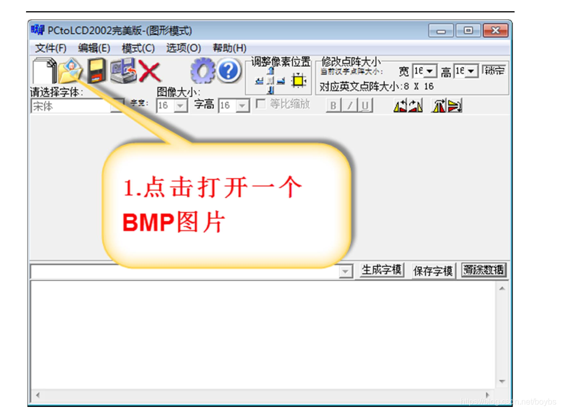
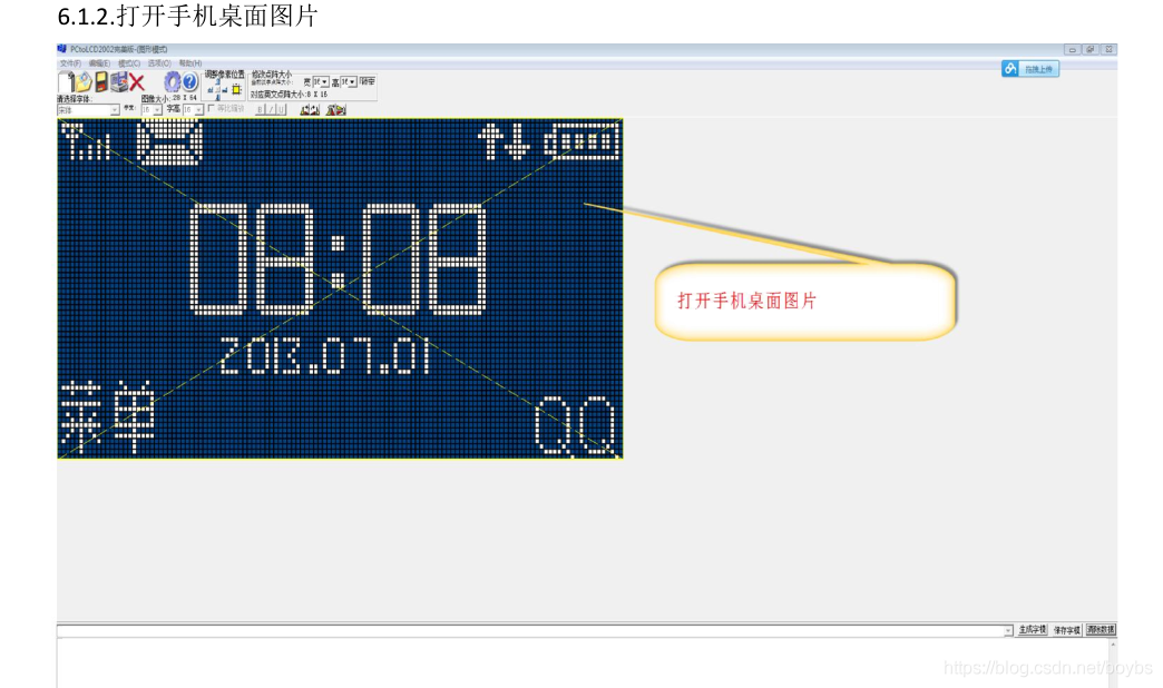
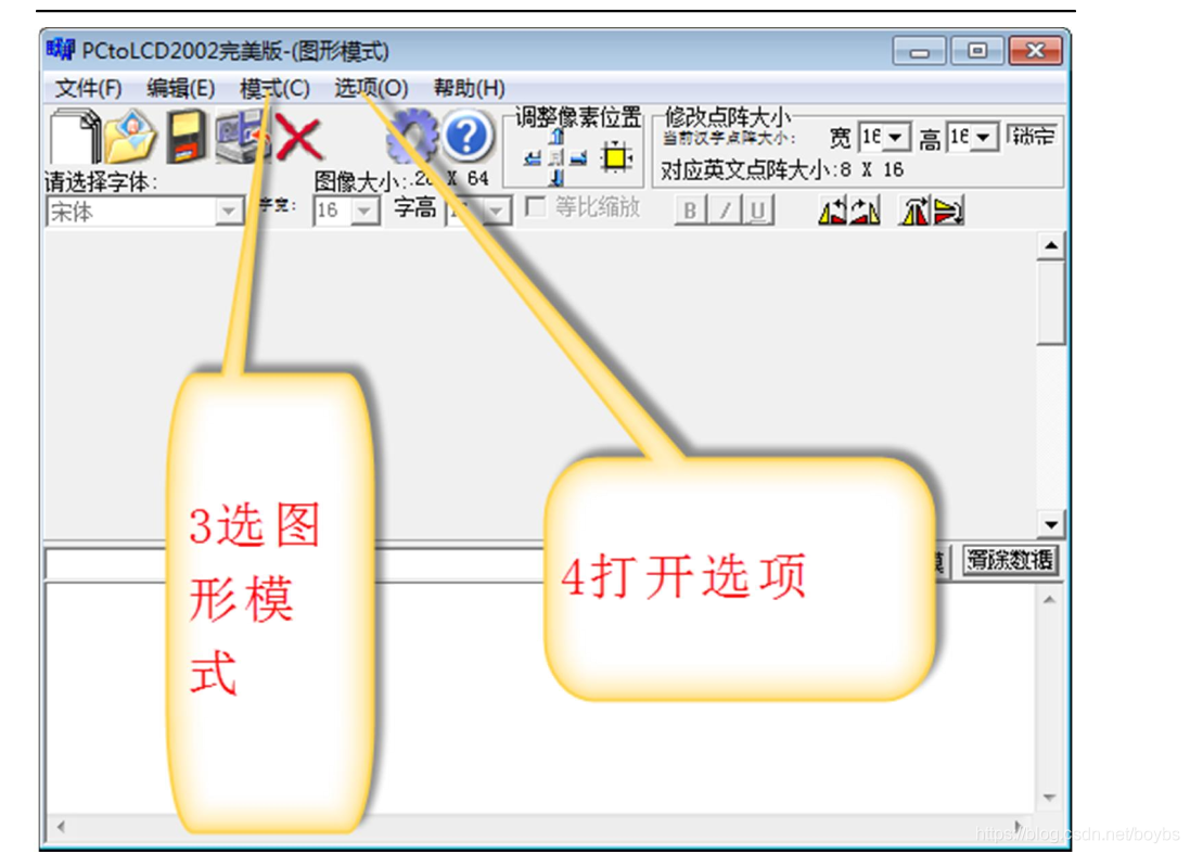
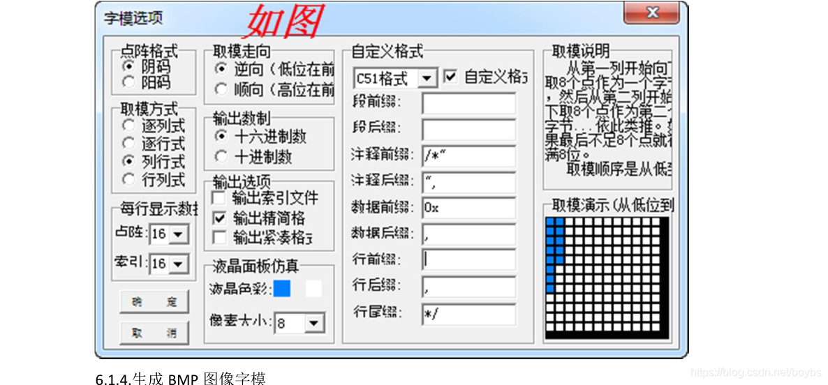
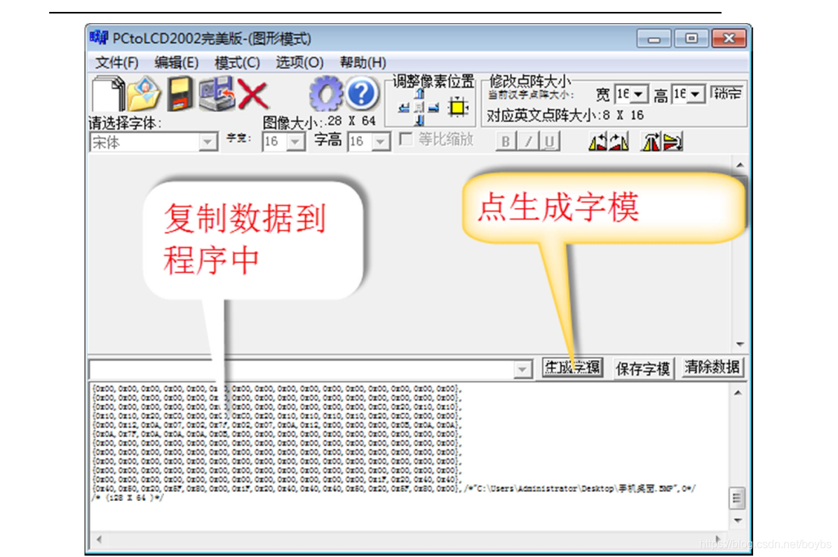
Description of mold taking:
There are three kinds of mold taking. One is picture, character and Chinese character. The principle of mold taking is the same
Open pctolcd2002 for image mold taking Exe software