1) Experimental platform: punctual atom STM32MP157 development board
2) Purchase link: https://item.taobao.com/item.htm?&id=629270721801
3) Full set of experimental source code + manual + video download address: http://www.openedv.com/thread-318813-1-1.html
4) Official station B of punctual atom: https://space.bilibili.com/394620890
5) Punctual atom STM32MP157 technical exchange group: 691905614

Chapter 15 FIFO experiment of IP core
The full English name of FIFO is First In First Out. FIFO used in FPGA generally refers to a buffer with First In First Out characteristics for data storage, which is often used for data cache or high-speed asynchronous data interaction, that is, the so-called cross clock domain signal transmission. The difference between it and the internal RAM and ROM of FPGA is that there is no external read-write address line. It adopts the way of sequentially writing data and sequentially reading data, which is simple and convenient to use. The disadvantage is that it can not be read or written to a specified address by the address line like RAM and ROM. In this chapter, we will read and write test the FIFO IP core generated by Vivado software to introduce the use of Xilinx FIFO IP core.
This chapter includes the following parts:
15.1 introduction to FIFO IP core
15.2 experimental tasks
15.3 hardware design
15.4 program design
15.5 download verification
15.1 introduction to FIFO IP core
According to the clock domain of FIFO, FIFO can be divided into synchronous FIFO and asynchronous FIFO. Synchronous FIFO means that the read clock and write clock are the same clock, and the read and write operations occur temporarily at the edge of the clock. Asynchronous FIFO means that the read-write clocks are inconsistent, and the read-write clocks are independent of each other. The FIFO IP core of Xilinx can be configured as synchronous FIFO or asynchronous FIFO, and its signal block diagram is shown in the figure below. As can be seen from the figure, when it is configured to synchronize FIFO, only WR is used_ CLK, all input and output signals are synchronized with wr_clk signal. When it is configured as asynchronous FIFO, the write port and read port have independent clocks respectively, and all write related signals are synchronized with the write clock wr_clk, all read related signals are synchronized with the read clock rd_clk.
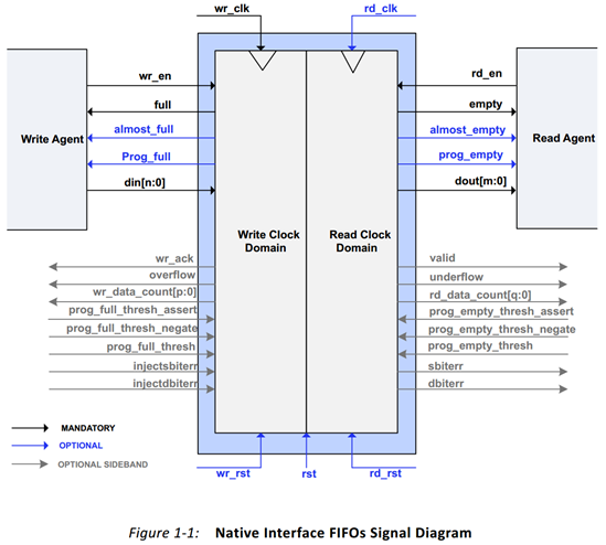
Figure 7.5.13.1 signal block diagram of Xilinx FIFO IP core
For FIFO, you need to know some common parameters:
FIFO width: data bit N of FIFO for one read / write operation.
Depth of FIFO: how many data with width of N bits can be stored in FIFO.
Empty flag: almost_empty. FIFO is about to be read empty.
Empty flag: empty. A signal sent by the FIFO state circuit when the FIFO is empty to prevent the read operation of the FIFO from continuing to read data from the FIFO, resulting in the reading of invalid data.
Full flag: almost_full. FIFO is about to be filled.
Full flag: full. A signal sent by the FIFO status circuit when the FIFO is full or about to be filled to prevent the FIFO write operation from continuing to write data to the FIFO, resulting in overflow.
Read clock: the clock followed when reading FIFO, which is triggered at the rising edge of each clock.
Write clock: the clock followed when writing FIFO, which is triggered at the rising edge of each clock.
Please note here that the "almost_empty" and "almost_full" signals are regarded as "empty" and "full" warning signals respectively. They will be pulled up one clock cycle ahead of the real empty and full.
For the basic knowledge of FIFO, it is enough to understand these first. Some people may wonder why there are synchronous FIFO and asynchronous FIFO, and what are their respective purposes. Synchronous FIFO and asynchronous FIFO have different functions. Synchronous FIFO is often used for data caching of synchronous clock, and asynchronous FIFO is often used for data signal transmission across clock domain. For example, data data1 under clock domain A is transmitted to asynchronous clock domain B. when data1 is A continuous change signal, if it is directly transmitted to clock domain B, it may lead to non reception, That is, there will be A series of problems including metastable problems in the acquisition process. Using asynchronous FIFO can synchronize the data in different clock domains to the required clock domain.
15.2 experimental tasks
The experimental task of this section is to use Vivado to generate FIFO IP core and realize the following functions: when FIFO is empty, write data to FIFO, and the amount of data written is consistent with FIFO depth, that is, FIFO is full; Then read the data from the FIFO until the FIFO is read empty, so as to introduce the use of FIFO IP core in detail.
15.3 hardware design
The experiment in this chapter only uses the input clock signal and key reset signal, and does not use other hardware peripherals.
In this experiment, the pin allocation of each port signal is shown in the table below.
Table 15.3.1 pin allocation of IP test
Signal name direction pin port description level standard
sys_clk input U18 system clock, 50Mhz LVCMOS33
sys_rst_n input N16 system reset, low effective LVCMOS33
The corresponding XDC constraint statements are as follows:
create_clock -period 20.000 -name clk [get_ports sys_clk]
set_property -dict {PACKAGE_PIN U18 IOSTANDARD LVCMOS33} [get_ports sys_clk]
set_property -dict {PACKAGE_PIN N16 IOSTANDARD LVCMOS33} [get_ports sys_rst_n]
15.4 program design
According to the experimental task requirements and the idea of modular design, we need the following four modules: FIFO IP core, write FIFO module, read FIFO module and top-level instantiation module to realize the signal interaction of the first three modules. Because FIFO is mostly used for signal processing across clock domain, in this experiment, we use asynchronous FIFO to introduce the creation and use of dual clock FIFO IP core in detail. In order to facilitate your understanding, here we use the system clock to drive the read / write clock. The functional block diagram of the system is shown in the figure below:
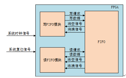
Figure 7.5.13.1 system block diagram
First, create a file called ip_fifo project. Next, we create fifo IP core. Click "IP Catalog" in the "Flow Navigator" column on the left side of Vivado software, and the "IP Catalog" button and the pop-up "IP Catalog" window after clicking are shown in the following figure.
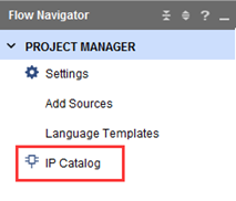
Figure 7.5.13.2 "IP Catalog" button
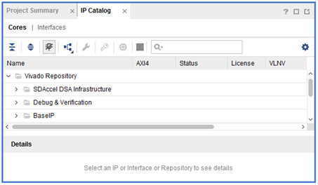
Figure 7.5.13.3 "IP Catalog" window
In the "IP Catalog" window, enter the keyword "fifo" in the search bar. At this time, Vivado will automatically find the IP core name matching the keyword. Double click "FIFO Generator", as shown in the following figure.
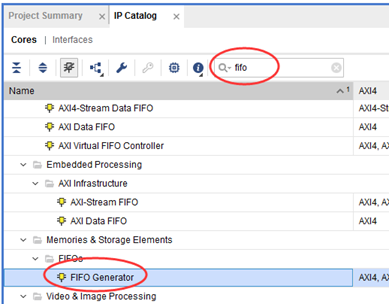
Figure 7.5.13.4 enter keywords in the search bar
The Customize IP window pops up, as shown in the following figure.
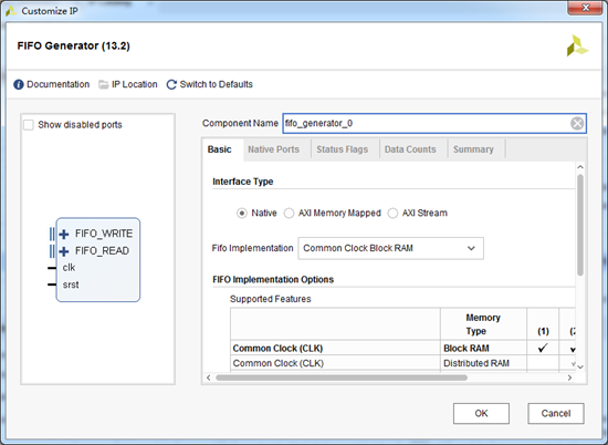
Figure 7.5.13.5 "Customize IP" window
The next step is to configure the clock parameters of the IP core.
Set the name of the IP component in the "Component Name" column at the top, and keep the default here. In the first "Basic" tab, the "Interface Type" option is used to select the type of FIFO interface. Here, we select the default "Native", that is, the traditional FIFO interface. The "Fifo Implementation" option is used to select whether we want to implement synchronous FIFO or asynchronous FIFO and which resources to use to implement FIFO. Here, we select "Independent Clocks Block RAM", that is, asynchronous FIFO implemented using block ram. As shown in the figure below.
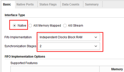
Figure 7.5.13.6 "Basic" tab
Next is the "Native Ports" tab, which is used to set the parameters of FIFO ports. The "Read Mode" option is used to set the Read Mode when reading FIFO. Here, we select the default "Standard FIFO". The column "Data Port Parameters" is used to set the width of the data bus of the read-write port and the depth of the FIFO. The Write Width "Write Width" is set to 8 bits and the Write Depth "Write Depth" is set to 256. Note that at this time, the actual depth that the FIFO IP core can achieve is 255; Although the Read Width "Read Width" can be set to a bit width different from the Write Width, and at this time, the Read Depth "Read Depth" will be passively and automatically set to the corresponding value according to the above three parameters; However, we still set the Read Width "Read Width" to the same bit width as the Write Width "Write Width", which is also the most commonly used case in practical applications. Since we only observe the reading and writing of FIFO, we can uncheck the "Reset Pin" option at the bottom. Other settings can remain the default, as shown in the following figure.
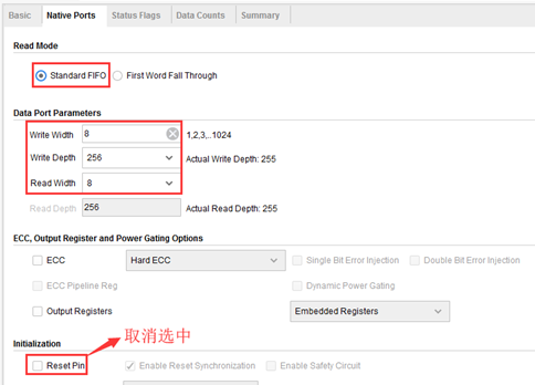
Figure 7.5.13.7 "Native Ports" tab
The "Status Flags" tab is used to set user-defined interfaces or special input ports. Here we use the two signals "about to write full" and "about to read empty", so we check them and keep the others by default, as shown in the figure below.
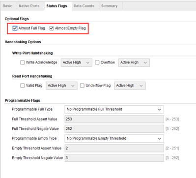
Figure 7.5.13.8 "Status Flags" tab
The "Data Counts" tab is used to set the output signal of data count in FIFO, which indicates how many valid data are currently stored in FIFO. In order to observe the read / write process more conveniently, here we turn on the Data Counts of the read / write port, and set the bit width of the count bus to full bit width, i.e. 8 bits, as shown in the figure below.
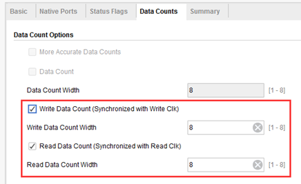
Figure 7.5.13.9 "Data Counts" tab
The final "Summary" tab is a Summary of all the previous configurations. Here, we can directly click "OK", as shown in the figure below.
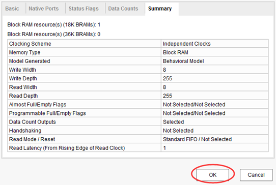
Figure 7.5.13.10 "Summary" tab
Then the "Generate output products" window pops up. We can directly click "Generate", as shown in the figure below.
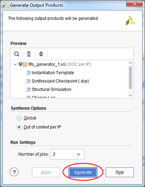
Figure 7.5.13.11 "Genarate Output Products" window
Then we can see the run "fifo_generator_0_synth_1" corresponding to the IP core in the "out of context module runs" column of the "Design Run" window. Its synthesis process is independent of the synthesis of the top-level design, so we can see that it is being synthesized, as shown in the following figure.
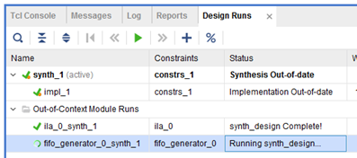
Figure 7.5.13.12 "fifo_generator _0_synth_1" run
In the process of out of context synthesis, we can carry out RTL coding. First, open the IP core instantiation template. In the IP Sources tab of the Source window, click IP - fifo_generator _0 - instantiation template successively, and we can see the file fifo_generator_0.veo, which is a read-only verilog instantiation template file automatically generated by the IP core. Double click to open it, as shown in the following figure.
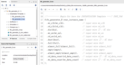
Figure 7.5.13.13 "fifo_generator_0.veo" file
We create a verilog source file named ip_fifo.v. As a top-level module, its code is as follows:
1  module ip_fifo(
2      input    sys_clk ,  // clock signal
3      input    sys_rst_n  // Reset signal
4  );
5
6  //wire define
7  wire         fifo_wr_en         ;  // FIFO write enable signal
8  wire         fifo_rd_en         ;  // FIFO read enable signal
9  wire  [7:0]  fifo_din           ;  // Data written to FIFO
10 wire  [7:0]  fifo_dout          ;  // Data read from FIFO
11 wire         almost_full        ;  // FIFO will be full
12 wire         almost_empty       ;  // FIFO will empty the signal
13 wire         fifo_full          ;  // FIFO full signal
14 wire         fifo_empty         ;  // FIFO null signal
15 wire  [7:0]  fifo_wr_data_count ;  // Data count of FIFO write clock field
16 wire  [7:0]  fifo_rd_data_count ;  // Data count in FIFO read clock field
17
18 //*****************************************************
19 //**                    main code
20 //*****************************************************
21
22 //Instantiated FIFO IP core
23 fifo_generator_0  fifo_generator_0 (
24     .wr_clk        ( sys_clk            ),  // input wire wr_clk
25     .rd_clk        ( sys_clk            ),  // input wire rd_clk
26
27     .wr_en         ( fifo_wr_en         ),  // input wire wr_en
28     .rd_en         ( fifo_rd_en         ),  // input wire rd_en
29
30     .din           ( fifo_din           ),  // input wire [7 : 0] din
31     .dout          ( fifo_dout          ),  // output wire [7 : 0] dout
32
33     .almost_full   (almost_full         ),  // output wire almost_full
34     .almost_empty  (almost_empty        ),  // output wire almost_empty
35     .full          ( fifo_full          ),  // output wire full
36     .empty         ( fifo_empty         ),  // output wire empty
37
38  .wr_data_count ( fifo_wr_data_count ),  // output wire [7 : 0] wr_data_count
39  .rd_data_count ( fifo_rd_data_count )   // output wire [7 : 0] rd_data_count
40 );
41
42 //Example write FIFO module
43 fifo_wr  u_fifo_wr(
44     .clk            ( sys_clk    ),   // Write clock
45     .rst_n          ( sys_rst_n  ),   // Reset signal
46
47     .fifo_wr_en     ( fifo_wr_en )  , // fifo write request
48     .fifo_wr_data   ( fifo_din    ) , // Data written to FIFO
49     .almost_empty   ( almost_empty ), // fifo will empty the signal
50     .almost_full    ( almost_full  )  // fifo will be full
51 );
52
53 //Example reading FIFO module
54 fifo_rd  u_fifo_rd(
55     .clk          ( sys_clk    ),      // Read clock
56     .rst_n        ( sys_rst_n  ),      // Reset signal
57
58     .fifo_rd_en   ( fifo_rd_en ),      // fifo read request
59     .fifo_dout    ( fifo_dout  ),      // Data output from FIFO
60     .almost_empty ( almost_empty ),    // fifo will empty the signal
61     .almost_full  ( almost_full  )     // fifo will be full
62 );
63
64 //Instantiated ILA IP core
65 ila_0  ila_0 (
66  .clk    ( sys_clk            ), // input wire clk
67
68  .probe0 ( fifo_wr_en         ), // input wire [0:0]  probe0
69  .probe1 ( fifo_rd_en         ), // input wire [0:0]  probe1
70  .probe2 ( fifo_din           ), // input wire [7:0]  probe2
71  .probe3 ( fifo_dout          ), // input wire [7:0]  probe3
72  .probe4 ( fifo_empty         ), // input wire [0:0]  probe4
73  .probe5 ( almost_empty       ), // input wire [0:0]  probe5
74  .probe6 ( fifo_full          ), // input wire [0:0]  probe6
75  .probe7 ( almost_full        ), // input wire [0:0]  probe7
76  .probe8 ( fifo_wr_data_count ), // input wire [7:0]  probe8
77  .probe9( fifo_rd_data_count  )  // input wire [7:0]  probe9
78 );
79
80 endmodule
The top-level module mainly instantiates the FIFO IP core, write FIFO module and read FIFO module. In addition, this experiment also generates and instantiates an ILA IP core for online acquisition and observation of the signals of the top-level module.
Write FIFO module FIFO_ wr. The code of V source file is as follows:
1  module fifo_wr(
2      input                  clk    ,          // clock signal
3      input                  rst_n  ,          // Reset signal
4
5      input                  almost_empty,     // FIFO will empty the signal
6      input                  almost_full ,     // FIFO will be full
7      output    reg          fifo_wr_en ,      // FIFO write enable
8      output    reg  [7:0]   fifo_wr_data      // Data written to FIFO
9  );
10
11 //reg define
12 reg  [1:0]  state            ;  //Action state
13 reg         almost_empty_d0  ;  //almost_empty delay one beat
14 reg         almost_empty_syn ;  //almost_empty delay two beats
15 reg  [3:0]  dly_cnt          ;  //Delay counter
16 //*****************************************************
17 //**                    main code
18 //*****************************************************
19
20 //Because almost_empty signal belongs to FIFO clock reading domain
21 //So synchronize it to the write clock field
22 always@( posedge clk ) begin
23  if( !rst_n ) begin
24      almost_empty_d0  <= 1'b0 ;
25      almost_empty_syn <= 1'b0 ;
26  end
27  else begin
28      almost_empty_d0  <= almost_empty ;
29      almost_empty_syn <= almost_empty_d0 ;
30  end
31 end
32
33 //Write data to FIFO
34 always @(posedge clk ) begin
35     if(!rst_n) begin
36         fifo_wr_en   <= 1'b0;
37         fifo_wr_data <= 8'd0;
38         state        <= 2'd0;
39      dly_cnt      <= 4'd0;
40     end
41     else begin
42         case(state)
43             2'd0: begin
44                 if(almost_empty_syn) begin  //If FIFO is detected, it will be read empty (the next shot will be empty)
45                     state <= 2'd1;          //It enters the delay state
46                 end
47                 else
48                     state <= state;
49             end
50          2'd1: begin
51                 if(dly_cnt == 4'd10) begin  //Delay 10 beats
52                                             //The reason is that there is a delay in updating the internal status signal of FIFO IP core
53                                             //Delay 10 beats to wait for the status signal to update
54                     dly_cnt    <= 4'd0;
55                  state      <= 2'd2;        //Start write operation
56                  fifo_wr_en <= 1'b1;        //Turn on write enable
57              end
58              else
59                  dly_cnt <= dly_cnt + 4'd1;
60             end
61          2'd2: begin
62                 if(almost_full) begin      //Wait for the FIFO to be full (the next shot will be full)
63                     fifo_wr_en   <= 1'b0;  //Turn off write enable
64                     fifo_wr_data <= 8'd0;
65                     state        <= 2'd0;  //Return to the first state
66                 end
67                 else begin                 //If FIFO is not full
68                     fifo_wr_en   <= 1'b1;  //The write enable is continuously turned on
69                     fifo_wr_data <= fifo_wr_data + 1'd1;  //And the write data value continues to accumulate
70                 end
71             end
72          default : state <= 2'd0;
73         endcase
74     end
75 end
76
77 endmodule
fifo_ The core part of WR module is a small state machine that continuously circulates the state. If FIFO is detected to be empty, it will be delayed by 10 beats first. Note here that since the update of internal signal of FIFO is delayed compared with the actual data read / write operation, the purpose of delaying 10 beats is to wait for the empty / full state signal of FIFO After updating the data count signal and other signals, the FIFO write operation can be carried out. If it is full, it will return to state 0, that is, wait for the FIFO to be read empty for the next round of write operation.
Read FIFO module FIFO_ The code of the rd.v source file is as follows:
1  module fifo_rd(
2      input               clk          ,   // clock signal
3      input               rst_n        ,   // Reset signal
4
5      input        [7:0]  fifo_dout    ,   // Data read from FIFO
6      input               almost_full  ,   // FIFO will be full
7      input               almost_empty ,   // FIFO will empty the signal
8      output  reg         fifo_rd_en       // FIFO read enable
9  );
10
11 //reg define
12 reg  [1:0]  state           ;  //state
13 reg         almost_full_d0  ;  //almost_full delay one beat
14 reg         almost_full_syn ;  //almost_full delay two beats
15 reg  [3:0]  dly_cnt         ;  //Delay counter
16
17 //*****************************************************
18 //**                    main code
19 //*****************************************************
20
21 //Because FIFO_ The full signal belongs to the FIFO write clock domain
22 //Therefore, it should be synchronized to the read clock domain
23 always@( posedge clk ) begin
24  if( !rst_n ) begin
25      almost_full_d0  <= 1'b0 ;
26      almost_full_syn <= 1'b0 ;
27  end
28  else begin
29      almost_full_d0  <= almost_full ;
30      almost_full_syn <= almost_full_d0 ;
31  end
32 end
33
34 //Read FIFO data
35 always @(posedge clk ) begin
36     if(!rst_n) begin
37         fifo_rd_en <= 1'b0;
38      state      <= 2'd0;
39      dly_cnt    <= 4'd0;
40     end
41     else begin
42         case(state)
43             2'd0: begin
44                 if(almost_full_syn)        //If FIFO is detected to be full
45                     state <= 2'd1;         //It enters the delay state
46                 else
47                     state <= state;
48             end
49          2'd1: begin
50                 if(dly_cnt == 4'd10) begin //Delay 10 beats
51                                            //The reason is that there is a delay in updating the internal status signal of FIFO IP core
52                                            //Delay 10 beats to wait for the status signal to update
53                     dly_cnt <= 4'd0;
54                  state   <= 2'd2;          //Start read operation
55              end
56              else
57                  dly_cnt <= dly_cnt + 4'd1;
58             end
59          2'd2: begin
60                 if(almost_empty) begin     //Wait for the FIFO to be read empty (the next shot will be empty)
61                     fifo_rd_en <= 1'b0;    //Turn off read enable
62                     state      <= 2'd0;    //Return to the first state
63                 end
64                 else                       //If FIFO is not read empty
65                     fifo_rd_en <= 1'b1;    //The read enable is continuously turned on
66             end
67          default : state <= 2'd0;
68         endcase
69     end
70 end
71
72 endmodule
The code structure of the read module is almost the same as that of the write module. It also uses a small state machine that continuously circulates the state to control the operation process. The reader should be able to understand it easily with reference to the code, which will not be repeated here.
We simulate the code. In TestBench, just send the clock reset signal. TB files are as follows:
1  `timescale 1ns / 1ps
2  module tb_ip_fifo( );
3      // Inputs
4      reg sys_clk;
5      reg sys_rst_n;
6
7  // Instantiate the Unit Under Test (UUT)
8  ip_fifo  u_ip_fifo (
9          .sys_clk         (sys_clk),
10         .sys_rst_n       (sys_rst_n)
11     );
12
13 //Genarate the clk
14 parameter PERIOD = 20;
15 always begin
16     sys_clk = 1'b0;
17     #(PERIOD/2) sys_clk = 1'b1;
18     #(PERIOD/2);
19 end
20
21 initial begin
22     // Initialize Inputs
23     sys_rst_n = 0;
24     // Wait 100 ns for global reset to finish
25     #100  ;
26     sys_rst_n = 1;
27     // Add stimulus here
28 end
29
30 endmodule
The simulation waveform of turning to read after full write is shown in the following figure:
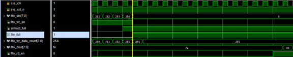
Figure 7.5.13.14 Vivado simulation waveform 1
It can be seen from the waveform diagram that when 255 data are written, fifo_ The full signal will be pulled up. After the delay, fifo_ rd_ The en write enable signal is pulled high. After one beat, it starts to send the data in fifo to fifo_ On the dout port.
The simulation waveform of turning to read after full write is shown in the following figure:
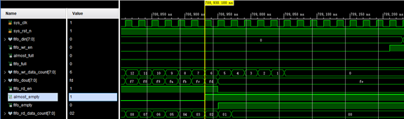
Figure 7.5.13.15 Vivado simulation waveform 2
It can be seen from the waveform diagram that after reading 255 data, fifo_empty signal will be pulled up. After the delay, fifo_ wr_ The en write enable signal is pulled high and continues to write data to fifo after one beat.
15.5 download verification
Compile the project and generate a bitstream Bit file, bitstream Download the bit file to Zynq.
After downloading, the "hw_ila_1" Dashboard window will automatically appear in Vivado. As shown in the figure below:
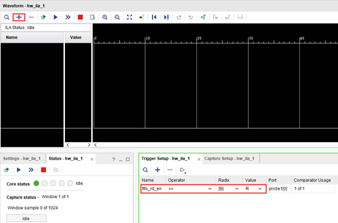
Figure 7.5.13.1 adding probe signal to waveform window
Add relevant probe signals to the waveform window. Here we have finished adding signals by clicking "+" in the upper left corner of "hw_ila_1" Dashboard window. At the same time, we add the "fifo_rd_en" signal to the trigger window in the lower right corner of the window and set it as the rising edge trigger,
Click the trigger button in the upper left corner, as shown in the following figure:
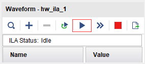
Figure 7.5.13.2 trigger button
Finally, you can see the data captured by ILA. The expanded waveform is shown in the figure below:
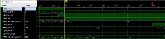
Figure 7.5.13.3 captured waveform
It can be seen from the captured waveform that its logical behavior is consistent with that in the simulation waveform, which proves that our code correctly realizes the expected function