
Introduction to TLC5615
TLC5615 is a product launched by Texas Instruments. It is a digital to analog converter with serial interface. The communication adopts three wire SPI protocol. Its output is voltage type, and the maximum output voltage is twice the reference voltage. The configuration is simple. There is no need to configure too many registers. It only needs a single 5V power supply to work
TLC5615 communication sequence
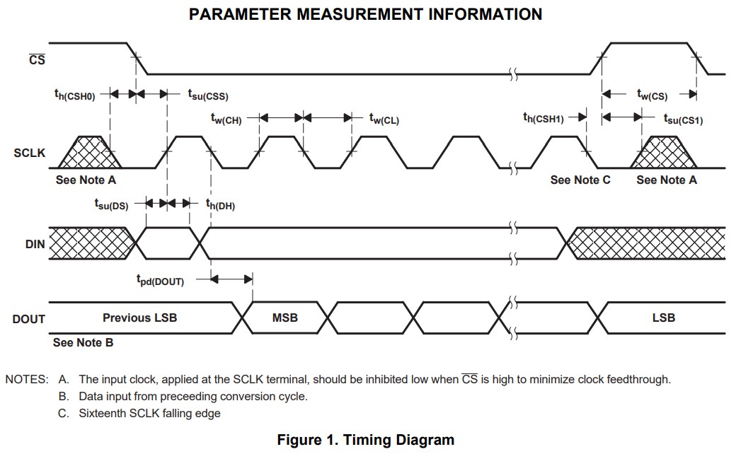
Through the above sequence diagram, we can quickly write the program of the underlying logic. This time, we only test the output specified voltage, so we only need to use the sequence of CS, SCLK and DIN pins. If only one module is driven, CS can also be directly grounded. At this time, we only need to occupy two IO ports of the single chip microcomputer to operate normally
Configuration of communication data
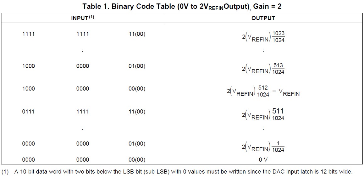
Find the above binary code table in the data manual. It can be known that the value of the last two bits is fixed to 0 (because the DAC input latch is 12 bits). The first ten bits of data determine the OUTPUT voltage. Its calculation formula can be seen in the OUTPUT on the right. If the approximate workflow is clear, the program burning test can be started
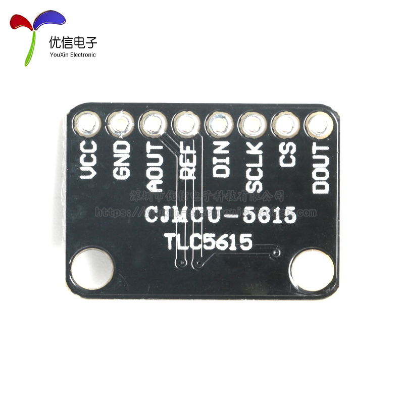
TLC5615 module
For hardware, please refer to the pin description below and the pin diagram of the module
| Pin name | Function description |
|---|---|
| VCC | Positive power supply terminal, 4.5 ~ 5.5V, usually 5V |
| GND | Simulated |
| AOUT | DAC analog voltage output |
| REF | Reference power input |
| DIN | Serial data input |
| SCLK | Serial clock input |
| CS | The chip selects the through end, and the low level is effective |
| DOUT | Serial data output for cascading |
There are eight pins on the top, of which REF and DOUT do not need to be used. See the schematic diagram of the module below to find several required parameters
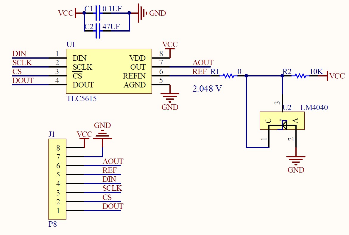
DOUT is used in cascade. It is not used at present, so it does not need to be connected. It can be seen in the schematic diagram that the module uses an LM4040 chip to provide a 2.048V voltage reference source for TLC5615, which is why we do not need an external reference source. Similarly, the voltage value of 2.048 needs to be used for subsequent calculation
51 single chip microcomputer drive
Post the complete code directly
#include<reg52.h>

sbit CS=P1^0;        //Chip selection port
sbit CLK =P1^1;      //Clock port
sbit DIN=P1^2;       //data input

void DA_OUTPUT(unsigned int value);   //Declare output voltage value function

void main(void)
{
	while(1)
	{
		DA_OUTPUT(250);
	}
}

void DA_OUTPUT(unsigned int value)
{
	unsigned char i;  //Define variables for loops
	value<<=6;        //The int type is 16 bits. If only 12 bits are needed, the high 4 bits will be removed for easy retrieval
	CS=0;             //Chip selection port
	CLK=0;

	/*Cycle 12 times, take out 12 bits and write them into the module register*/
	for(i = 0; i < 12; i++)
	{
		DIN=(bit)(value&0x8000);   //Take out the highest position
		CLK=1;
		value<<=1;
		CLK=0;
	}

	CS=1;
	CLK=0;             //Restore the default low state
}
The code of 51 is relatively short. sbit is used to define the port used at the top, which is simple and easy to modify. A function void Da is defined later_ OUTPUT(unsigned int value);
In this function, the input parameter call will directly change the output voltage of the module, and its corresponding voltage relationship is the output voltage V o u t V_{out} Vout =2Vref ⋅ \cdot ⋅ v a l u e 1024 \frac{value}{1024} 1024 value, where value is the value we input in the function and Vref is the reference voltage of 2.048 V o u t V_{out} Vout is the output voltage of Aout port
After simplification, we need the output voltage V o u t V_{out} The function value that needs to be input when Vout + V o u t 0.004 \frac{Vout}{0.004} 0.004Vout, i.e V o u t V_{out} Vout * 250. If we need TLC5615 module to output 1V voltage, we need to add parameter 250 to the function. Friends who are interested can also optimize the function
The default wiring can refer to the following table
| 51 single chip microcomputer | TLC5615 |
|---|---|
| 5V | VCC |
| GND | GND |
| P1.0 | CS |
| P1.1 | CLK |
| P1.2 | DIN |
If you need a code, you can leave a message email or private mail email below
arduino driver
arduino driver has a large number of libraries that can be called, which can save developers a lot of time. Here, we also use the way of calling libraries to drive and directly post the source code
#include "TLC5615.h"

TLC5615 TLC5615(2,3,4);  //CS--->2  CLK--->3   DIN--->4

void setup() {
  // put your setup code here, to run once:
    TLC5615.begin();
}

void loop() {
  // put your main code here, to run repeatedly:
    TLC5615.DA_OUTPUT(500);
}
The above also calls several functions in the library to realize the function of specified voltage output. Similar to 51 single chip microcomputer, I use amplification. I wrote a function void Da with the same function in the library_ OUTPUT(uint16_t value); To be used by users
You only need to write four pieces of code to realize the fixed voltage output (loop is generated by yourself). Remember to add the library before use. If you need the library or information, you can leave a message mailbox or private mail mailbox below
Code segment TLC5615 TLC5615(2,3,4); The TLC5615 object is declared, and its name can be customized. The parameters 2, 3 and 4 added later represent the CS, CLK and DIN ports used by the module respectively. Similarly, the definition can be modified as needed
TLC5615.begin(); Function is used to initialize the port used by TLC5615 defined earlier
Function TLC5615 DA_ OUTPUT(500); It is used to control the output voltage value of AOUT port, that is, the input value= V o u t V_{out} Vout * 250. The specific calculation process can refer to the driving part of 51 single chip microcomputer
Next, after the burning program is wired, you can measure whether the corresponding output voltage is corresponding. Refer to the following table for specific wiring
| arduino | TLC5615 |
|---|---|
| 5V | VCC |
| GND | GND |
| 2 | CS |
| 3 | CLK |
| 4 | DIN |
stm32 drive
The code of stm32 is a little more complicated. Here I will directly post main The code in C uses the single chip microcomputer model STM32F103C8 series. If a complete project is required, you can leave a message mailbox or private mail mailbox below
#include "pbdata.h"
#include"stm32f10x.h"

#define CS_1   GPIO_SetBits(Pin_group,CS_Pin)
#define CS_0   GPIO_ResetBits(Pin_group,CS_Pin)

#define CLK_1  GPIO_SetBits(Pin_group,CLK_Pin)
#define CLK_0	 GPIO_ResetBits(Pin_group,CLK_Pin)

#define DIN_1  GPIO_SetBits(Pin_group,DIN_Pin)
#define DIN_0	 GPIO_ResetBits(Pin_group,DIN_Pin)

/*Define pins to use*/
#define   CS_Pin    GPIO_Pin_6
#define   CLK_Pin   GPIO_Pin_7
#define   DIN_Pin   GPIO_Pin_8

/*Define the group of pins*/
#define   Pin_group   GPIOB

/*Defines the clock used*/
#define   Pin_RCC   RCC_APB2Periph_GPIOB

void GPIO_init(GPIO_TypeDef*GPIOx,u16 GPIO_Pin,GPIOMode_TypeDef Mode)
{
	GPIO_InitTypeDef GPIO_InitStruct;//Declare a structure initialized by a pin
	GPIO_InitStruct.GPIO_Mode=Mode;
	GPIO_InitStruct.GPIO_Pin=GPIO_Pin;
	GPIO_InitStruct.GPIO_Speed=GPIO_Speed_50MHz;
	GPIO_Init(GPIOB,&GPIO_InitStruct);
}

void DA_OUTPUT(uint16_t value)
{
	uint8_t i;
	value<<=6;
	CS_0;CLK_0;
	for(i = 0; i < 12; i++)
	{
		if(value&0x8000)
		{
			DIN_1;
		}
		else
		{
			DIN_0;
		}
		CLK_1;
		value<<=1;
		CLK_0;
	}
	CS_1;CLK_0;
}

int main(void)
{
	RCC_APB2PeriphClockCmd(Pin_RCC,ENABLE);
	GPIO_init(Pin_group,CS_Pin|CLK_Pin|DIN_Pin,GPIO_Mode_Out_PP);
	CS_1;CLK_0;DIN_0;
	while(1)
	{
		DA_OUTPUT(500);
	}
}
The code for controlling the pin connecting TLC5615 is as follows
/*Define pins to use*/
#define   CS_Pin    GPIO_Pin_6
#define   CLK_Pin   GPIO_Pin_7
#define   DIN_Pin   GPIO_Pin_8

/*Define the group of pins*/
#define   Pin_group   GPIOB

/*Defines the clock used*/
#define   Pin_RCC   RCC_APB2Periph_GPIOB
Control the pin, the GPIO group where the pin is located and the clock respectively. There is not much else to pay attention to. The output function void Da inside_ The function of output (uint16_t value) is exactly the same as that described in the above 51 single chip microcomputer or arduino driver
It needs to be up to stm32F4 or other MCU with faster clock speed. It should be noted that the driving timing may need to increase the delay. According to the timing in the manual, it may not be able to drive normally when the speed reaches 50ns or less
The default wiring can refer to the following table
| STM32F1 | TLC5615 |
|---|---|
| 5V | VCC |
| GND | GND |
| PB6 | CS |
| PB7 | CLK |
| PB8 | DIN |
summary
TLC5615 is an ADC device with simple timing. It is easy to use, easy to operate, and has a 10 bit resolution. It is relatively cost-effective. The above provides three common driving modes and programs of single chip microcomputer, and can modify the output square wave, sine wave, triangular wave, etc. based on the above program, Friends who need information program can leave a message or private mail email below. They will send it when they see it. Welcome to leave a message and exchange. We can learn from each other and make progress!