I am snowy fish, an FPGA enthusiast, and my research direction is FPGA architecture exploration.
Focus on official account [integrated circuit design course], pull you into "IC design exchange group".
Learn the modeling method of efga fabric through the only demo provided by FABulous.
1, Fabric Layout
First look at the demo:
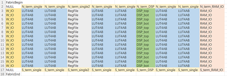
The layout of Fabric is defined between the keywords FabricBegin and FabricEnd.
The basic unit is a tile. If it is null, no code will be generated and it is reserved for padding. Multiple tiles can also be combined into one tile, called Supertiles. As shown in the figure above, a DSP is composed of two tiles (DSP_top and DSP_bot).
2, Configuration parameter definition
First look at the demo:
ParametersBegin
ConfigBitMode,frame_based # default is FlipFlopChain,,frame_based
#FrameBitsPerRow,32,"# we configure an entire configuration frame over the full height of the device (like Virtex-II) and we write FrameBitsPerRow bits per, well, tile=CLB height"
#MaxFramesPerCol,20
#Package,use work.my_package.all;
GenerateDelayInSwitchMatrix,80
MultiplexerStyle,custom,#,custom,generic
SuperTileEnable,TRUE,#,TRUE,FALSE
ParametersEnd
Some Flow configuration keywords are defined between the keywords ParametersBegin and parameterend.
Format: < key >, < value >
- ConfigBitMode,[frame_based|FlipFlopChain]
Select frame_based configuration method or FlipFlopChain configuration method. At present, some open source FPGA modeling tools adopt the configuration method of trigger scan chain, while FABulous can choose two configuration methods and support reconfiguration.
After consulting elder martial brother, reconfiguration means to modify the circuit function of the target area without changing the circuit function of other areas of FPGA, that is, to replace the connection of the circuit in this area.
- FrameBitsPerRow, unsigned_int
- MaxFramesPerCol
- Package
- GenerateDelayInSwitchMatrix
- Multiplexerstyle, [custom|generic]: select the style of switch matrix MUX, whether to use custom or general template. This paper shows that PPA can be optimized through user-defined MUX.
- Hypertileenable, [true, false]: select whether to enable the hypertile function.
3, Tile definition
There are 13 tile s defined in this fabric. Next, analyze them one by one.
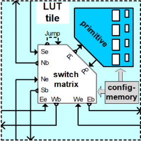
Firstly, a complete tile modeled by FABulous is introduced, including:
- Interconnect
- Central switch matrix
- Some basic modules
- Configuration module
3.1 LUT4AB
code:
TILE,LUT4AB #carry out
#direction,source_name,X-offset,Y-offset,destination_name,wires
NORTH,N1BEG,0,-1,N1END,4
NORTH,N2BEG,0,-1,N2MID,8
NORTH,N2BEGb,0,-1,N2END,8
NORTH,N4BEG,0,-4,N4END,4
NORTH,NN4BEG,0,-4,NN4END,4
NORTH,Co,0,-1,Ci,1,# carry
EAST,E1BEG,1,0,E1END,4
EAST,E2BEG,1,0,E2MID,8
EAST,E2BEGb,1,0,E2END,8
EAST,EE4BEG,4,0,EE4END,4
EAST,E6BEG,6,0,E6END,2
SOUTH,S1BEG,0,1,S1END,4
SOUTH,S2BEG,0,1,S2MID,8
SOUTH,S2BEGb,0,1,S2END,8
SOUTH,S4BEG,0,4,S4END,4
SOUTH,SS4BEG,0,4,SS4END,4
#SOUTH,NULL,0,1,Ci,1
WEST,W1BEG,-1,0,W1END,4
WEST,W2BEG,-1,0,W2MID,8
WEST,W2BEGb,-1,0,W2END,8
WEST,WW4BEG,-4,0,WW4END,4
WEST,W6BEG,-6,0,W6END,2
JUMP,J2MID_ABa_BEG,0,0,J2MID_ABa_END,4
JUMP,J2MID_CDa_BEG,0,0,J2MID_CDa_END,4
JUMP,J2MID_EFa_BEG,0,0,J2MID_EFa_END,4
JUMP,J2MID_GHa_BEG,0,0,J2MID_GHa_END,4
JUMP,J2MID_ABb_BEG,0,0,J2MID_ABb_END,4
JUMP,J2MID_CDb_BEG,0,0,J2MID_CDb_END,4
JUMP,J2MID_EFb_BEG,0,0,J2MID_EFb_END,4
JUMP,J2MID_GHb_BEG,0,0,J2MID_GHb_END,4
JUMP,J2END_AB_BEG,0,0,J2END_AB_END,4
JUMP,J2END_CD_BEG,0,0,J2END_CD_END,4
JUMP,J2END_EF_BEG,0,0,J2END_EF_END,4
JUMP,J2END_GH_BEG,0,0,J2END_GH_END,4
JUMP,JN2BEG,0,0,JN2END,8
JUMP,JE2BEG,0,0,JE2END,8
JUMP,JS2BEG,0,0,JS2END,8
JUMP,JW2BEG,0,0,JW2END,8
JUMP,J_l_AB_BEG,0,0,J_l_AB_END,4
JUMP,J_l_CD_BEG,0,0,J_l_CD_END,4
JUMP,J_l_EF_BEG,0,0,J_l_EF_END,4
JUMP,J_l_GH_BEG,0,0,J_l_GH_END,4
JUMP,NULL,0,0,GND,1
JUMP,NULL,0,0,VCC,1
JUMP,J_SR_BEG,0,0,J_SR_END,1
JUMP,J_EN_BEG,0,0,J_EN_END,1
BEL,LUT4c_frame_config.vhdl,LA_
BEL,LUT4c_frame_config.vhdl,LB_
BEL,LUT4c_frame_config.vhdl,LC_
BEL,LUT4c_frame_config.vhdl,LD_
BEL,LUT4c_frame_config.vhdl,LE_
BEL,LUT4c_frame_config.vhdl,LF_
BEL,LUT4c_frame_config.vhdl,LG_
BEL,LUT4c_frame_config.vhdl,LH_
BEL,MUX8LUT_frame_config.vhdl
MATRIX,LUT4AB_switch_matrix.vhdl
EndTILE
Here, I import the Verilog demo provided by FABulous (which is inconsistent with the tile description above, but can be used as a reference) into Vivado for compilation for easy understanding.
The compiled LUT4AB block diagram is as follows:
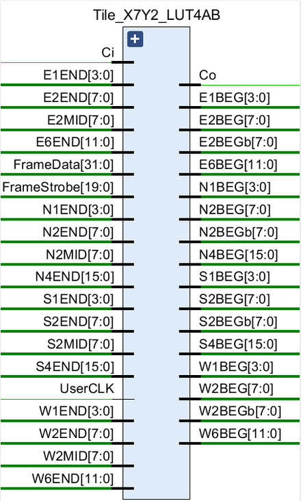
- The keyword NORTH/EAST/SOUTH/WEST is used to specify the port
- JUMP is used to set the tile's internal lut4ab_ switch_ The jumper of matrix is shown in the figure below:
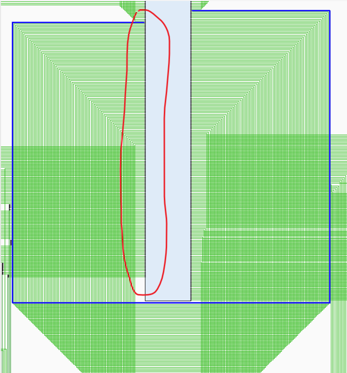
These lines are connected from one end of the switch matrix to the other, and are not connected outside the tile.
- The vhdl code used by BEL to bind the basic module (verilog code should also be supported)
This demo LUT4AB tile contains the following modules:
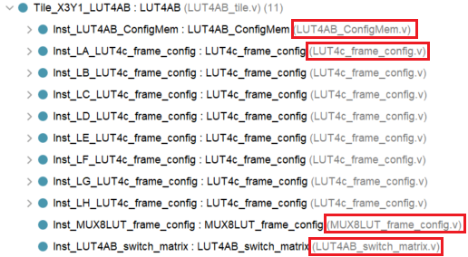
There are four basic modules.
- MATRIX is used to set the RTL description code of the switch MATRIX.
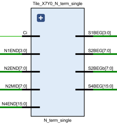
3.2 N_term_single
TILE,N_term_single
#direction,source_name,X-offset,Y-offset,destination_name,wires
NORTH,NULL,0,-1,N1END,4
NORTH,NULL,0,-1,N2MID,8
NORTH,NULL,0,-1,N2END,8
NORTH,NULL,0,-4,N4END,4
NORTH,NULL,0,-4,NN4END,4
NORTH,NULL,0,-1,Ci,1
SOUTH,S1BEG,0,1,NULL,4
SOUTH,S2BEG,0,1,NULL,8
SOUTH,S2BEGb,0,1,NULL,8
SOUTH,S4BEG,0,4,NULL,4
SOUTH,SS4BEG,0,4,NULL,4
MATRIX,N_term_single_switch_matrix.vhdl
EndTILE

This module contains only one switch matrix and no other modules.
Compiled schematic:
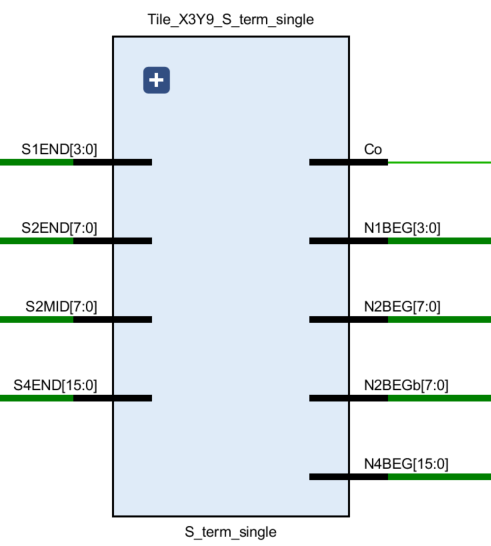
3.3 S_term_single
TILE,S_term_single
#direction,source_name,X-offset,Y-offset,destination_name,wires
NORTH,N1BEG,0,-1,NULL,4
NORTH,N2BEG,0,-1,NULL,8
NORTH,N2BEGb,0,-1,NULL,8
NORTH,N4BEG,0,-4,NULL,4
NORTH,NN4BEG,0,-4,NULL,4
NORTH,Co,0,-1,NULL,1
SOUTH,NULL,0,1,S1END,4
SOUTH,NULL,0,1,S2MID,8
SOUTH,NULL,0,1,S2END,8
SOUTH,NULL,0,4,S4END,4
SOUTH,NULL,0,4,SS4END,4
JUMP,NULL,0,0,GND,1
MATRIX,S_term_single_switch_matrix.vhdl
EndTILE
Compiled schematic diagram:
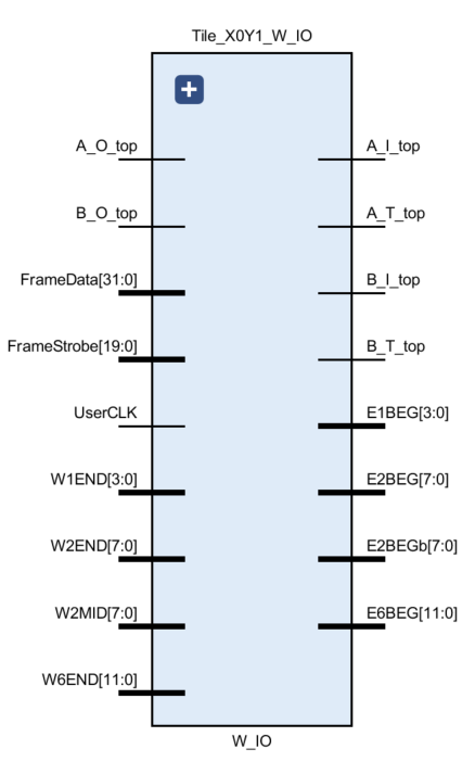
3.4 W_IO
TILE,W_IO
#direction,source_name,X-offset,Y-offset,destination_name,wires
EAST,E1BEG,1,0,NULL,4
EAST,E2BEG,1,0,NULL,8
EAST,E2BEGb,1,0,NULL,8
EAST,EE4BEG,4,0,NULL,4
EAST,E6BEG,6,0,NULL,2
WEST,NULL,-1,0,W1END,4
WEST,NULL,-1,0,W2MID,8
WEST,NULL,-1,0,W2END,8
WEST,NULL,-4,0,WW4END,4
WEST,NULL,-6,0,W6END,2
JUMP,NULL,0,0,GND,1
JUMP,NULL,0,0,VCC,1
BEL,IO_1_bidirectional_frame_config_pass.vhdl,A_
BEL,IO_1_bidirectional_frame_config_pass.vhdl,B_
BEL,Config_access.vhdl,A_config_
BEL,Config_access.vhdl,B_config_
MATRIX,W_IO_switch_matrix.vhdl
EndTILE
Compiled schematic diagram:
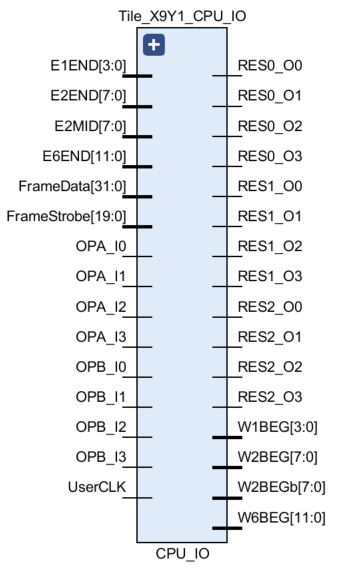
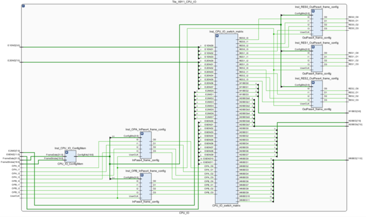
3.5 CPU_IO
TILE,CPU_IO
#direction,source_name,X-offset,Y-offset,destination_name,wires
EAST,NULL,1,0,E1END,4
EAST,NULL,1,0,E2MID,8
EAST,NULL,1,0,E2END,8
EAST,NULL,4,0,EE4END,4
EAST,NULL,6,0,E6END,2
WEST,W1BEG,-1,0,NULL,4
WEST,W2BEG,-1,0,NULL,8
WEST,W2BEGb,-1,0,NULL,8
WEST,WW4BEG,-4,0,NULL,4
WEST,W6BEG,-6,0,NULL,2
JUMP,NULL,0,0,GND,1
BEL,InPass4_frame_config.vhdl,OPA_  ,,
BEL,InPass4_frame_config.vhdl,OPB_  ,,
BEL,OutPass4_frame_config.vhdl,RES0_  ,,
BEL,OutPass4_frame_config.vhdl,RES1_  ,,
BEL,OutPass4_frame_config.vhdl,RES2_  ,,
MATRIX,CPU_IO_switch_matrix.vhdl
EndTILE
Compiled schematic diagram:
- For more technical articles and learning materials, please pay attention to my official account: integrated circuit design course.
- Unified across the platform: [snowy fish]