Design of Experimental f4a 8-bit 12-instruction Hard Wiring CPU
Model machine is a compact model of a computer. It can understand the structure and function of the whole computer, understand the structure of CPU, memory, interrupt controller, interface, and realize the logic and interface relationship between components. The main content of this course design is to design an 8-bit model computer using the internal programmable resources of Intel's EPF10K10LC84-4. The main purpose of this course design is to make students master the understanding of the concept of "time-space" in computer work through the design and debugging of 8-bit model machines at the component level, so as to clearly set up the whole concept of computer, and to train students'ability to analyze and solve practical problems, while enhancing students' practical ability.
1. Experimental Purpose
(1) Integrate the contents of each chapter of this course, through the comprehensive use of knowledge, to deepen the understanding of the working principle and interrelation of various functional components of computer system, to deepen the understanding of the concept of "time-space" in computer work, so as to clearly establish the concept of computer as a whole;
(2) Learn the basic steps and methods for designing and debugging computers, and improve the basic skills of using software simulation tools such as Quartus and integrated circuits;
(3) To cultivate the independent ability of scientific research and obtain the practice and experience of engineering design and assembly debugging.
2. Design Requirements
Design an 8-bit model computer for a hard wiring controller, complete the design and debug successfully in VHDL language
3. Experimental Principles
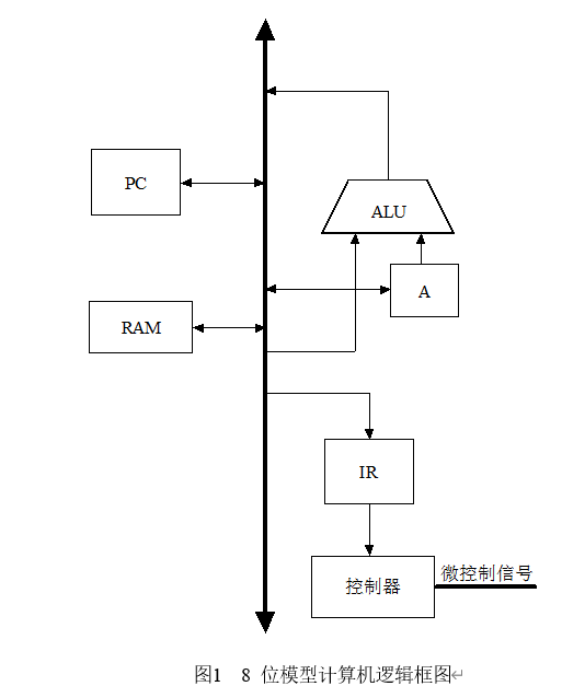
With the controller as the center, the first controller obtains instructions from the instruction register, compiles the instructions, outputs the micro-control signals, controls the operation of ALU, adds one to PC, and takes out the data operation from RAM. After the operation, the result is stored in RAM through the data bus, reads out the next instruction in the instruction register, and loops in turn.
4. Design Content
5. Display of CPU circuit diagrams
6. Model Machine Simulation Diagram Composed of Six Modules
Connect the six modules into a whole. It generates control signals, that is, the control signals generated by the controller, to control the operation of each module. It can detect the signals sent by other parts, coordinate each part to complete the specified tasks according to the instructions, so its output is the control signals of the major control signals, that is, the control signals of the controllers involved earlier.
7. Analysis of test programs, waveforms and corresponding relations with instructions in ram and data operation process
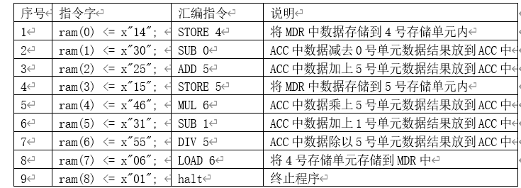
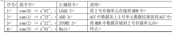
(1) Test program
(2) Correspondence analysis of waveform diagrams and data changes, step by step, operation by step, and part by part, and analysis of data operation process.
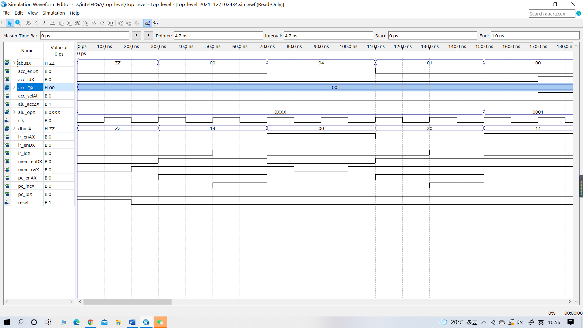
Read instructions
Step One:PC Pass the instruction address to the address bus MAR

abus in,If the transmission is pc Value in,For increments from 0000 to 001(9)Number of

The address bus value is 0000 at this time,0000

Step 2:Send read commands to main memory

whenever PC When the value of,PC_enAX 1,That is the sign PC Visit MAR

In this system,PC Pass command address directly to RAM

Step 3:take MAR The memory unit specified is passed to the MDR

By the first directive in the first Ordinance,The data bus is 0001 at this time,0100,That is RAM Data corresponding to storage unit No. 0;

Step 4:take MDR To IR,

here ir_ldx 1,Flag is written to data

Step 5:Give the opcode part of the instruction to CU

CU use IR Last 4 digits(4 To 7 bits)As opcode,Decoding;

Instruction 0001,0100

Opcode 0001,Memory Directive

Step 6:Form the next instruction

PC+1

here,Address bus 0000,0001
Execution cycle (for example, number of instructions)
Memory Directive

Step One:Address code of the command to be(Top Four)From the Address Bus section to MAR

Instruction 0001,0100

Address code is 0100

The value of the address bus is 0000 at this time,0100

here pc_enAx 1,sign cu towards RAM Write data

Step 2:Read instructions to main memory

here mem_rwX 1

Step 3:take MDR Write data from MAR In the specified main memory unit;

here MDR Not an instruction,But data

The data bus is 0000 at this time,0000

here mem_rw 0,Flag Write Operation

Upcoming data 0000,0000 Write to Unit 4;
7. Other test programs, Waveform Graphs and corresponding relationship analysis with instructions, data operation process analysis
(2) Corresponding relationship analysis of waveform diagram and data change step by step, step by step, operation by step, part by part, and data operation process analysis.
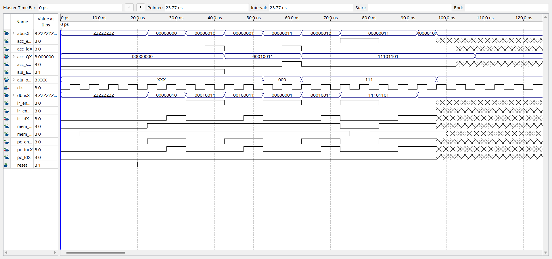
LOAD 2
PC For 0000,0000
PC Pass command address directly to MAR,MAR Passed to by data bus RAM;
The address bus is 0000 at this time,0000
 Get the instruction of storage unit 0 and pass through the data bus to MDR
 The data bus is 0000 at this time,0010 Instruction is 0000,0010
 Opcode 0000,LOAD
 Address number is 0010,2 Number storage bit
 Opcode part to CU;
Address code part to MAR,MAR From the address bus RAM,And pass the data to the MDR and ACC
 The address bus is 0000 at this time,0010
 The data bus is 0001 at this time,0010
 here ACC_QX For 0001,0010

ADD 3
PC For 0000,0001
PC Pass command address directly to MAR,MAR Passed to by data bus RAM;
The address bus is 0000 at this time,0001
 Get the instruction of storage unit 1 and pass through the data bus to MDR
 The data bus is 0010 at this time,0011 Instruction is 0010,0011
 Opcode 0010,ADD
 Address number 0011,3 Number storage
 Opcode part to CU;control ALU Perform addition operation
 here ALU_OP For 000
 Yes ACC Content Reverse,ACC_QX 1110,1110
 Address code part to MAR,MAR From the address bus RAM,And pass the data to the MDR and ACC
 The address bus is 0000 at this time,0011
 The data bus is 0000 at this time,0001
 here cu operation ALU_OP 111,ALU Complete the addition of two trees
 Data bus values are:0001,0010;1110,1110;0000,0001;0010,0011;
Get and 0010,0011 Output to ACC
 here ACC_QX For 0010,0011

STORE 2
PC For 0000,0010
PC Pass command address directly to MAR,MAR Passed to by data bus RAM;
The address bus is 0000 at this time,0010
 Get the instructions for storage unit 2 and pass through the data bus to MDR
 The data bus is 0001 at this time,0010 Instruction 0001,0010
 Opcode 0001,STORE
 Address number is 0010,2 Number storage bit
 Opcode part to CU;
Address code part to MAR,MAR From the address bus RAM,And pass the data to the MDR and ACC
 The address bus is 0000 at this time,0010
 The data bus is 1100 at this time,1110
 here mem_rw 0,Write operation

HALT
PC For 0000,0011
PC Pass command address directly to MAR,MAR Passed to by data bus RAM;
The address bus is 0000 at this time,0011
 Get the instructions for storage unit 4 and pass through the data bus to MDR
 The data bus is 0000 at this time,0001 Instruction is 0000,0001
 Opcode is HALT,Program End
VIII. EXPERIMENTAL CODE
1, Accumulative register accumulator
library IEEE;
use IEEE.std_logic_1164.all;
use IEEE.std_logic_unsigned.all;
entity accumulator is ----Declare external entity interfaces
port (
clk, en_D, ld, selAlu, reset: in STD_LOGIC; --clock signal
aluD: in STD_LOGIC_VECTOR(7 downto 0);
dBus: inout STD_LOGIC_VECTOR(7 downto 0);
q: out STD_LOGIC_VECTOR(7 downto 0)
);
end accumulator;
architecture accArch of accumulator is
signal accReg: STD_LOGIC_VECTOR(7 downto 0);
begin
process(clk) begin
if clk'event and clk = '1' then
if reset = '1' then
accReg <= "00000000";
elsif ld = '1' and selAlu = '1' then
accReg <= aluD;
elsif ld = '1' and selAlu = '0' then
accReg <= dBus;
end if;
end if;
end process;
dBus <= accReg when en_D = '1' else
"ZZZZZZZZ";
q <= accReg;
end accArch;
2, Arithmetic Operator ALU
library IEEE;
use IEEE.std_logic_1164.all;
use IEEE.std_logic_unsigned.all;
entity alu is -----Entity Claim External Interface
port (
op: in STD_LOGIC_VECTOR(3 downto 0); --Select the type of control operation
accD: in STD_LOGIC_VECTOR(7 downto 0); -- 8-bit data for accumulator
dBus: in STD_LOGIC_VECTOR(7 downto 0); -- Data bus for operations
result: out STD_LOGIC_VECTOR(7 downto 0); --Output of results
accZ: out STD_LOGIC
);
end alu;
architecture aluArch of alu is
begin
result <= (not accD) + "00000001" when op ="0000" else
accD + dBus when op ="0001" else
accD+"10000000" when op="0010" else
dBus+"10000000" when op="0011" else
(not accD)-"00000001" when op="0100" else
accD-dBus when op="0101" else
accD*dBus when op="0110" else
accD*(not dBus) when op="0111" else
accD AND dBus when op="1010" else
accD NAND dBus when op="1011" else
accD OR dBus when op="1100" else
accD NOR dBus when op="1101" else
accD XNOR dBus when op="1110" else
NOT accD when op="1111" else
"00000000";
accZ <= not (accD(0) or accD(1) or accD(2) or accD(3) or
accD(4) or accD(5) or accD(6) or accD(7)
);
end aluArch;
3, Hard Wiring Controller ( controller)
library IEEE;
use IEEE.std_logic_1164.all;
entity controller is ----Declare entity external interfaces
port (
clk, reset:
in STD_LOGIC;
mem_enD, mem_rw:
out STD_LOGIC;
pc_enA, pc_ld, pc_inc: out STD_LOGIC;
ir_enA, ir_enD, ir_ld: out STD_LOGIC;
ir_load, ir_store, ir_add: in STD_LOGIC;
ir_sub,ir_mul,ir_div: in STD_LOGIC;
ir_and,ir_or, ir_not: in STD_LOGIC;
ir_neg, ir_halt, ir_branch: in STD_LOGIC;
acc_enD, acc_ld, acc_selAlu: out STD_LOGIC;
alu_op: out STD_LOGIC_VECTOR(2 downto 0)
);
end controller;
architecture controllerArch of controller is
type state_type is ( reset_state,
fetch0, fetch1,
load0, load1,
store0, store1,
add0, add1,
sub0, sub1,
mul0, mul1,
div0, div1,
and0, and1,
or0, or1,
not0, not1,
negate0, negate1,
halt,
branch0, branch1
);
signal state: state_type;
begin
process(clk) begin
if clk'event and clk = '1' then
if reset = '1' then state <= reset_state;
else
case state is
when reset_state => state <= fetch0;
when fetch0 => state <= fetch1;
when fetch1 =>
if ir_load = '1' then state <= load0;
elsif ir_store = '1' then state <= store0;
elsif ir_add = '1' then state <= add0;
elsif ir_sub = '1' then state <= sub0;
elsif ir_mul = '1' then state <= mul0;
elsif ir_div = '1' then state <= div0;
elsif ir_and = '1' then state <= and0;
elsif ir_or = '1' then state <= or0;
elsif ir_not = '1' then state <= not0;
elsif ir_neg = '1' then state <= negate0;
elsif ir_halt = '1' then state <= halt;
elsif ir_branch = '1' then state <= branch0;
end if;
when load0 => state <= load1;
when load1 => state <= fetch0;
when store0 => state <= store1;
when store1 => state <= fetch0;
when add0 => state <= add1;
when add1 => state <= fetch0;
when sub0 => state <= sub1;
when sub1 => state <= fetch0;
when mul0 => state <= mul1;
when mul1 => state <=fetch0;
when div0 => state <=div1;
when div1 => state <=fetch0;
when and0 => state <=and1;
when and1 => state <=fetch0;
when or0 => state <=or1;
when or1 => state <=fetch0;
when not0 => state <=not1;
when not1 => state <=fetch0;
when negate0 => state <= negate1;
when negate1 => state <= fetch0;
when halt => state <= halt;
when branch0 => state <= branch1;
when branch1 => state <= fetch0;
when others => state <= halt;
end case;
end if;
end if;
end process;
process(clk) begin -- special process for memory write timing
if clk'event and clk = '0' then
if state = store0 then
mem_rw <= '0';
else
mem_rw <= '1';
end if;
end if;
end process;
mem_enD <= '1' when state = fetch0 or state = fetch1 or
state = load0 or state = load1 or
state = add0 or state = add1 or
state = sub0 or state = sub1 or
state = mul0 or state = mul1 or
state = div0 or state = div1 or
state = and0 or state = and1 or
state = or0 or state = or1 else '0';
pc_enA <= '1' when state = fetch0 or
state = fetch1 else '0';
pc_ld <= '1' when state = branch0
else '0';
pc_inc <= '1' when state = fetch1
else '0';
ir_enA <= '1' when state = load0 or
state = load1 or state = store0 or
state = store1 or state = add0 or
state = add1 or state = sub0 or
state = sub1 or state = mul0 or
state = mul1 or state = div0 or
state = div1 or state = and0 or
state = and1 or state = or0 or
state = or1 else '0';
ir_enD <= '1' when state = branch0
else '0';
ir_ld <= '1' when state = fetch1
else '0';
acc_enD <= '1' when state = store0 or state = store1 else '0';
acc_ld <= '1' when state = load1 or state = add1 or state = negate1
or state = sub1 or state = mul1 or state = div1
or state = not1 or state = or1 or state = not1 else '0';
acc_selAlu <='1' when state = add1 or state = negate1 or state = sub1 or
state = mul1 or state = div1 or state = not1 or
state = or1 or state = not1 else '0';
alu_op <= "000" when state = add0 or state = add1
else "001" when state = sub0 or state = sub1
else "010" when state = mul0 or state = mul1
else "011" when state = div0 or state = div1
else "100" when state = negate0 or state = negate1
else "101" when state = and0 or state = and1
else "110" when state = or0 or state = or1
else "111" when state = not0 or state = not1;
--alu_op <= "01" when state = add0 or state = add1 else "00";
end controllerArch;
4, Instruction Register instruction_register
library IEEE;
use IEEE.std_logic_1164.all;
entity instruction_register is ----Declare entity external interfaces
port (
clk, en_A, en_D, ld, reset: in STD_LOGIC;
aBus: out STD_LOGIC_VECTOR(7 downto 0); ----Data bus output
dBus: inout STD_LOGIC_VECTOR(7 downto 0);
load, store, add, sub,mul,div,andd,orr,nott,neg, halt, branch: out STD_LOGIC
);
end instruction_register;
architecture irArch of instruction_register is
signal irReg: STD_LOGIC_VECTOR(7 downto 0);
begin
process(clk) begin
if clk'event and clk = '0' then -- load on falling edge
if reset = '1' then
irReg <= "00000000";
elsif ld = '1' then
irReg <= dBus;
end if;
end if;
end process;
aBus <= "0000" & irReg(3 downto 0) when en_A = '1' else
"ZZZZZZZZ";
dBus <= "0000" & irReg(3 downto 0) when en_D = '1' else
"ZZZZZZZZ";
load <= '1' when irReg(7 downto 4) = "0000" else '0';
store <= '1' when irReg(7 downto 4) = "0001" else '0';
add <= '1' when irReg(7 downto 4) = "0010" else '0';
sub <= '1' when irReg(7 downto 4) = "0011" else '0';
mul <= '1' when irReg(7 downto 4) = "0100" else '0';
div <= '1' when irReg(7 downto 4) = "0101" else '0';
neg <= '1' when irReg = "0110" & "0000" else '0';
andd <= '1' when irReg (7 downto 4) = "0111" else '0';
orr <= '1' when irReg (7 downto 4) = "1000" else '0';
nott <= '1' when irReg (7 downto 4) = "1001" else '0';
halt <= '1' when irReg = "1010" & "0001" else '0';
branch <= '1' when irReg(7 downto 4) = "1011" else '0';
end irArch;
5. Program counter program_counter
library IEEE;
use IEEE.std_logic_1164.all;
use IEEE.std_logic_unsigned.all;
entity program_counter is
port (
clk, en_A, ld, inc, reset: in STD_LOGIC;
aBus: out STD_LOGIC_VECTOR(7 downto 0); --Data bus output
dBus: in STD_LOGIC_VECTOR(7 downto 0); --Data Bus Input
);
end program_counter;
architecture pcArch of program_counter is
signal pcReg: STD_LOGIC_VECTOR(7 downto 0);
begin
process(clk) begin
if clk'event and clk = '1' then
if reset = '1' then
pcReg <= "00000000";
elsif ld = '1' then
pcReg <= dBus;
elsif inc = '1' then
pcReg <= pcReg + "00000001";
end if;
end if;
end process;
aBus <= pcReg when en_A = '1' else "ZZZZZZZZ";
end pcArch;
6, storage RAM
library IEEE;
use IEEE.std_logic_1164.all;
use IEEE.std_logic_arith.all;
entity ram is
port (
r_w, en, reset: in STD_LOGIC;
aBus: in STD_LOGIC_VECTOR(7 downto 0); ----Data Bus Input
dBus: inout STD_LOGIC_VECTOR(7 downto 0)
);
end ram;
architecture ramArch of ram is
type ram_typ is array(0 to 63) of STD_LOGIC_VECTOR(7 downto 0);
signal ram: ram_typ;
begin
process(
en, reset, r_w, aBus, dBus
) begin
if reset = '1' then
ram(0) <= x"14";
ram(1) <= x"30";
ram(2) <= x"25";
ram(3) <= x"15";
ram(4) <= x"46";
ram(5) <= x"31";
ram(6) <= x"55";
ram(7) <= x"06";
ram(8) <= x"01";
elsif r_w = '0' then
ram(conv_integer(unsigned(aBus))) <= dBus;
end if;
end process;
dBus <= ram(conv_integer(unsigned(aBus)))
when reset = '0' and en = '1' and r_w = '1' else
"ZZZZZZZZ";
end ramArch;
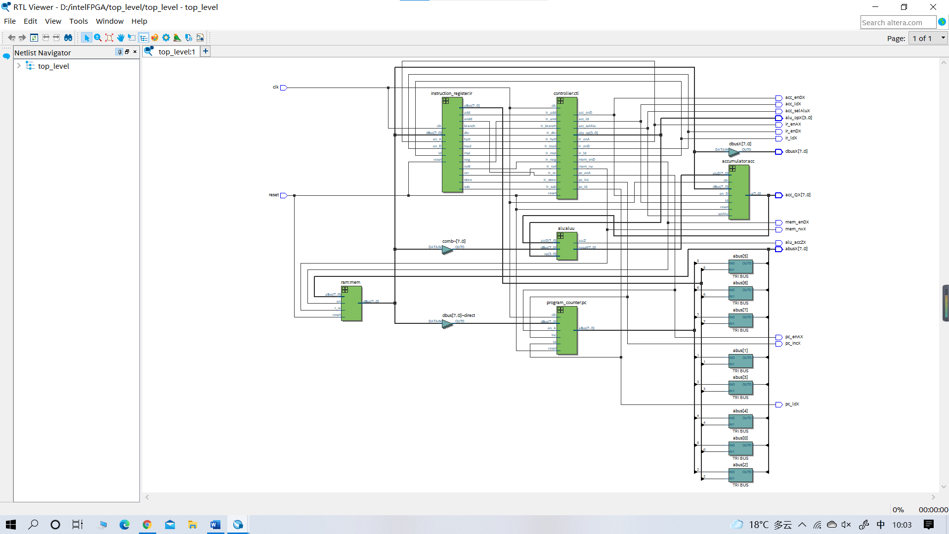
7, A model machine consisting of six modules(top_level)
library IEEE;
use IEEE.std_logic_1164.all;
entity top_level is ----Declare entity external interfaces
port (
clk, reset:
in STD_LOGIC;
abusX: out STD_LOGIC_VECTOR(7 downto 0); --Data bus output
dbusX: out STD_LOGIC_VECTOR(7 downto 0);
mem_enDX, mem_rwX:
out STD_LOGIC;
pc_enAX, pc_ldX, pc_incX:
out STD_LOGIC;
ir_enAX, ir_enDX, ir_ldX:
out STD_LOGIC;
acc_enDX, acc_ldX, acc_selAluX:
out STD_LOGIC;
acc_QX: out STD_LOGIC_VECTOR(7 downto 0);
alu_accZX: out STD_LOGIC;
alu_opX: out STD_LOGIC_VECTOR(2 downto 0)
);
end top_level;
architecture topArch of top_level is
component program_counter
port (
clk, en_A, ld, inc, reset: in STD_LOGIC;
aBus: out STD_LOGIC_VECTOR(7 downto 0);
dBus: in STD_LOGIC_VECTOR(7 downto 0)
);
end component;
component instruction_register
port (
clk, en_A, en_D, ld, reset: in STD_LOGIC;
aBus: out STD_LOGIC_VECTOR(7 downto 0);
dBus: inout STD_LOGIC_VECTOR(7 downto 0);
load, store, add, sub,mul,div,neg,andd,orr,nott, halt, branch: out STD_LOGIC
);
end component;
component accumulator
port (
clk, en_D, ld, selAlu, reset: in STD_LOGIC;
aluD: in STD_LOGIC_VECTOR(7 downto 0);
dBus: inout STD_LOGIC_VECTOR(7 downto 0);
q: out STD_LOGIC_VECTOR(7 downto 0)
);
end component;
component alu
port (
op: in STD_LOGIC_VECTOR(2 downto 0);
accD: in STD_LOGIC_VECTOR(7 downto 0);
dBus: in STD_LOGIC_VECTOR(7 downto 0);
result: out STD_LOGIC_VECTOR(7 downto 0);
accZ: out STD_LOGIC
);
end component;
component ram
port (
r_w, en, reset: in STD_LOGIC;
aBus: in STD_LOGIC_VECTOR(7 downto 0);
dBus: inout STD_LOGIC_VECTOR(7 downto 0)
);
end component;
component controller
port (
clk, reset: in STD_LOGIC;
mem_enD, mem_rw: out STD_LOGIC;
pc_enA, pc_ld, pc_inc: out STD_LOGIC;
ir_enA, ir_enD, ir_ld: out STD_LOGIC;
ir_load, ir_store, ir_add: in STD_LOGIC;
ir_sub, ir_mul, ir_div: in STD_LOGIC;
ir_and, ir_or, ir_not: in STD_LOGIC;
ir_neg, ir_halt, ir_branch: in STD_LOGIC;
acc_enD, acc_ld, acc_selAlu: out STD_LOGIC;
alu_op: out STD_LOGIC_VECTOR(2 downto 0)
);
end component;
signal abus: STD_LOGIC_VECTOR(7 downto 0);
signal dbus: STD_LOGIC_VECTOR(7 downto 0);
signal mem_enD, mem_rw: STD_LOGIC;
signal pc_enA, pc_ld, pc_inc: STD_LOGIC;
signal ir_enA, ir_enD, ir_ld: STD_LOGIC;
signal ir_load, ir_store, ir_add: STD_LOGIC;
signal ir_sub, ir_mul, ir_div: STD_LOGIC;
signal ir_and, ir_or, ir_not: STD_LOGIC;
signal ir_negate, ir_halt, ir_branch: STD_LOGIC;
signal acc_enD, acc_ld, acc_selAlu: STD_LOGIC;
signal acc_Q: STD_LOGIC_VECTOR(7 downto 0);
signal alu_op: STD_LOGIC_VECTOR(2 downto 0);
signal alu_accZ: STD_LOGIC;
signal alu_result: STD_LOGIC_VECTOR(7 downto 0);
begin
pc: program_counter port map(clk, pc_enA, pc_ld, pc_inc, reset, abus, dbus);
ir: instruction_register port map(clk, ir_enA, ir_enD, ir_ld, reset, abus,dbus,ir_load,ir_store,ir_add,ir_sub,ir_mul,ir_div,ir_and,ir_or,ir_not,ir_negate, ir_halt, ir_branch );
acc: accumulator port map(clk, acc_enD, acc_ld, acc_selAlu, reset, alu_result, dbus, acc_Q);
aluu: alu port map(alu_op, acc_Q, dbus, alu_result, alu_accZ);
mem: ram port map(mem_rw, mem_enD, reset, abus, dbus);
ctl: controller port map (
clk, reset, mem_enD, mem_rw, pc_enA, pc_ld, pc_inc,
ir_enA, ir_enD, ir_ld, ir_load, ir_store, ir_add,ir_sub,
ir_mul,ir_div,ir_and,ir_or,ir_not,
ir_negate, ir_halt, ir_branch,acc_enD,
acc_ld, acc_selAlu, alu_op
);
abusX <= abus;
dbusX <= dbus;
mem_enDX <= mem_enD;
mem_rwX <= mem_rw;
pc_enAX <= pc_enA;
pc_ldX <= pc_ld;
pc_incX <= pc_inc;
ir_enAX <= ir_enA;
ir_enDX <= ir_enD;
ir_ldX <= ir_ld;
acc_enDX <= acc_enD;
acc_ldX <= acc_ld;
acc_selAluX <= acc_selAlu;
acc_QX <= acc_Q;
alu_opX <= alu_op;
alu_accZX <= alu_accZ;
end topArch;