sketch
PCF8591 is a single chip, single power supply, low power consumption, 8-bit CMOS digital converter
According to the acquisition device, it has four analog inputs, one analog output and one
Serial I2C bus interface.
Serial I / O via I2C bus
schematic diagram:
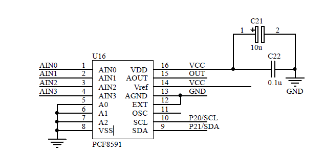
Pin definition:
| SYMBOL | PIN | DESCRIPTION | translation |
| AIN0 | 1 | analog inputs (A/D converter) | Analog input |
| AIN1 | 2 | ||
| AIN2 | 3 | ||
| AIN3 | 4 | ||
| A0 | 5 | hardware address | hardware address |
| A1 | 6 | ||
| A2 | 7 | ||
| VSS | 8 | negative supply voltage | Negative voltage |
| SDA | 9 | I2C-bus data input/output | IIC data line |
| SCL | 10 | I2C-bus clock input | IIC timeline |
| OSC | 11 | oscillator input/output | Oscillator input and output |
| EXT | 12 | external/internal switch for oscillator input | External / internal switch of oscillator input |
| AGND | 13 | analog ground | Analog grounding |
| VREF | 14 | voltage reference input | Reference voltage (VCC connected) |
| AOUT | 15 | analog output (D/A converter) | Analog output |
| VDD | 16 | positive supply voltage | Positive voltage |
Relevant address
IIC addressing device address
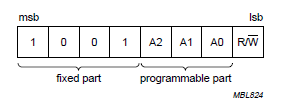
The first four bits are fixed as 1001. According to the schematic diagram, A2, A1 and A0 are grounded low-level 0; Therefore, the write address of PCF8591 is 0X90 and the read address is 0X91;
Control address
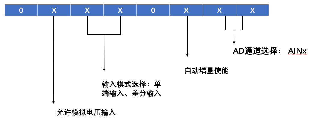
bit0-bit1: channel selection, 00 is AIN0 channel, 01 is AIN1 channel, 10 is AIN2 channel and 11 is AIN3 channel. According to the Blue Bridge Cup MCU development board, AIN0 is connected to the external A/D input channel of J3 row needle, AIN1 is connected to the photosensitive resistor, and AIN3 is connected to the RB2 potentiometer (adjustable resistor).
bit3: Auto increment enable bit (1 valid): if the auto increment flag is set to 1, the channel number will increase automatically after each A/D conversion.
bit5-bit6: input mode selection bits: 00 is single ended input, 01 is three differential inputs, 10 is single ended and differential mixed input, and 11 is two differential inputs; It is generally set as single ended input 00
bit7: run analog voltage input bit, and set 1 for conversion;
IIC timing analysis
Write operation:
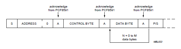
START - > Device Address - > address of write operation - > ACK of pcf8591 - > Control Byte - > ACK of pcf8591 - > data word - > ACK of pcf8591
Read operation:
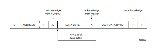
Single byte reading: START - > Device Address > > address of read operation > > ACK of pcf8591 - > read Data Byte - > ACK of host > > stop
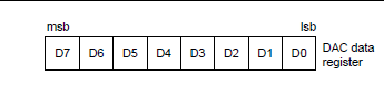
D/A conversion
Convert the digital quantity received on the bus into analog quantity and output it in AOUT. Mainly use the write operation of IIC to realize data writing, and then output the corresponding analog voltage.
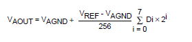
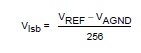
Calculation formula:
V
O
U
T
=
255
×
D
A
T
A
V
R
E
F
{V}_{OUT}=255\times \frac {DATA} {{V}_{REF}}
VOUT=255×VREFDATA
A / D conversion formula
The analog voltage input from AINx port is converted into digital quantity and sent to the bus. The data reading is mainly realized by IIC reading operation, and then the corresponding analog voltage is displayed.
Digital to analog conversion formula:
code:
1: AD conversion of photosensitive resistor and variable resistor, switching of S4 control mode
#include "reg52.h"
#include "iic.h"

sbit S4 = P3^3;
unsigned char Rd1 = 0; //Photoresistor AIN1
unsigned char Rd2 = 0;	//Adjustable resistor AIN3
unsigned char status = 0; //Key status record

unsigned char SMG_NoDot[19] = {0xc0,0xf9,0xa4,0xb0,0x99,0x92,0x82,0xf8,0x80,0x90,0x88,0x80,0xc6,0xc0,0x86,0x8e,0xbf,0x7f,0xff}; //0-9,A-F,'-','.'														   0x80,0x90,0x88,0x83,0xC6,0xA1,0x86,0x8E,0xbf};


//---------------------------------Simple delay function-------------------------
void Delay(unsigned int t)
{
 	while(t--);
}

void Delay500us()		//@12.000MHz
{
	unsigned char i, j;

	i = 6;
	j = 211;
	do
	{
		while (--j);
	} while (--i);
}
void Digital_Tube(unsigned char Position,unsigned char Typeface)    //Position is the position of the nixie tube (from left to right, starting with 0), and Typeface is the displayed word
{
  unsigned char Bit[8]={0x01,0x02,0x04,0x08,0x10,0x20,0x40,0x80};
	P2 = P2 & 0x1f | 0xc0;
	P0=Bit[Position];
	P2 = P2 & 0x1f | 0xe0;
	P0=Typeface;
	Delay500us();
	P0=0XFF;
	P2 = P2 & 0x1f ;	//Nixie tube shadow elimination
}
//---------------------------------Digital tube AD display----------------------
void Display_PCF8591(unsigned char channel,unsigned char dat)
{
	Digital_Tube(0,SMG_NoDot[16]);
	Digital_Tube(1,SMG_NoDot[channel]);
	Digital_Tube(2,SMG_NoDot[16]);
	Digital_Tube(3,0xff);
	Digital_Tube(4,0xff);
	Digital_Tube(5,SMG_NoDot[dat/100]);
	Digital_Tube(6,SMG_NoDot[dat/10%10]);
	Digital_Tube(7,SMG_NoDot[dat%10]);
}

//----------------------------Read photosensitive AD-----------------------------------

//The read operation address of PCF8591 device is 0x91; The write address is 0x90
//The photosensitive sensor is connected to AIN1, channel 1; The control register should write: 0x01.
//Potentiometer Rb2 is connected to AIN3, channel 3; The control register should write: 0x03.
void Read_Rd1_Data(void)
{
		 IIC_Start();					//IIC bus start signal
		 IIC_SendByte(0x90);	//Send PCF8591 device address write operation
		 IIC_WaitAck();			  //Waiting for response
		 IIC_SendByte(0x01);  //Send ain analog channel number 	  AIN3
		 IIC_WaitAck();				//Waiting for response
		 IIC_Stop();					//IIC bus stop signal

		 Display_PCF8591(1,Rd1);

		 IIC_Start();						//Start signal
		 IIC_SendByte(0x91);	  //Send PCF8591 device address read operation
		 IIC_WaitAck();					//Waiting for response
		 Rd1 = IIC_RecByte();		//Read data
		IIC_SendAck(1);				//Send non reply signal
		 IIC_Stop();						//IIC bus stop signal

		 Display_PCF8591(1,Rd1);
}

//-----------------------------Read sliding resistance AD-----------------------------
void Read_Rd2_Data(void)
{
		IIC_Start();	        //IIC bus start signal
		IIC_SendByte(0x90);	  //Send PCF8591 device address write operation
		IIC_WaitAck();			  //Waiting for response
		IIC_SendByte(0x03);	  //Send ain analog channel number 	  AIN3
		IIC_WaitAck();				 //Waiting for response
		IIC_Stop();						 //IIC bus stop signal

		Display_PCF8591(3,Rd2);

	  IIC_Start();//Start signal
		IIC_SendByte(0x91);	  //Send PCF8591 device address read operation
		IIC_WaitAck();			  //Waiting for response
		Rd2 = IIC_RecByte();  //Read data
		IIC_SendAck(1);				//Send non reply signal
		IIC_Stop();	  				//IIC bus stop signal

		Display_PCF8591(3,Rd2);
}

//----------------------------------Key switching control----------------------------
void Key_Tackle(void)
{
	 if(S4 == 0)
	 {
			Delay(20);
			if(S4 == 0)
			{
			 	if(status == 0)
				{
				 	status = 1;
					while(S4 == 0)
					{
						 Display_PCF8591(1,Rd1);
					}
				}

				else if(status == 1)
				{
				 	status = 0;
					while(S4 == 0)
					{
						 Display_PCF8591(3,Rd2);
					}

				}
			}
	 }
}

void main(void)
{
	Read_Rd1_Data(); //Photosensitive data acquisition is carried out by default when power on
	while(1)
	{
		Key_Tackle();
		if(status == 0)
		{
		 	 Read_Rd1_Data();
		}
		else
		{
		 	 Read_Rd2_Data();
		}
	}
}
2: Output quantitative analog voltage
On the right side of the development board, the D/A pin outputs analog voltage. The output voltage is related to the reference voltage of the chip, which may be a little smaller than the actual value. You need to fine tune it yourself.
#include "reg52.h"
#include "iic.h"

void Analog_Out(unsigned char DATA)
{
	 IIC_Start();					//IIC bus start signal
	 IIC_SendByte(0x90);	//Send PCF8591 device address write operation
	 IIC_WaitAck();			  //Waiting for response
	 IIC_SendByte(0X40);  //Send AIN analog channel number 	  AIN0 output mode
	 IIC_WaitAck();				//Waiting for response
		IIC_SendByte(DATA);  //Send data corresponding to analog voltage
		IIC_WaitAck();				//Waiting for response
	 IIC_Stop();					//IIC bus stop signal
}


void main(void)
{

	while(1)
	{
		 	 Analog_Out(255*3/5);
	}
}