1. PCF8591 module introduction
PCF8591 is a monolithic integrated, separately powered, low-power, 8-bit CMOS data acquisition device. PCF8591 has 4 analog inputs, 1 analog output and 1 serial I ² C bus interface.
The address, control and data signals input and output on the PCF8591 device are transmitted in serial mode through two-wire bidirectional I2C bus.
2. Circuit connection diagram
PCF8591 circuit connection diagram
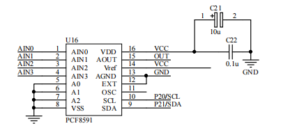
AIN0 ~ AIN3: analog signal input terminal.
A0 ~ A2: lower 3 bits of device address.
VSS: negative pole of power supply.
SDA and SCL: data line and clock line of I2C bus.
OSC: external clock input and internal clock output.
EXT: internal / external clock selection line, EXT is grounded when using internal clock.
AGND: analog signal ground.
VREF: reference power terminal.
AOUT: D/A conversion output terminal.
VDD: power terminal. (2.5~6V)
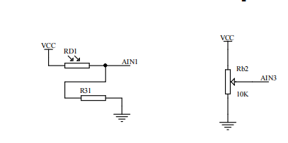
AINI is externally connected with a photosensitive resistor and a fixed value resistor, which reads the voltage at both ends of the fixed value resistor. Therefore, the stronger the illumination, the smaller the photosensitive resistor resistance, that is, the smaller the voltage, and then the R31 voltage increases. Therefore, in general, the read voltage increases with the increase of illumination.
AIN3 is externally connected with a potentiometer RB2, which reads the resistance of AIN3 to the grounding part, so the voltage decreases with the increase of resistance
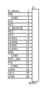
Here, two pins 18 and 19 of J3, one AIN0 is ADC reading and the other out is DAC output, which can be connected to external equipment. The out output value can be read through jumper cap connection.
3. Device address
Like AT24C0D, the three address pins A0, A1 and A2 of PCF8591 can be used for hardware address programming, that is, to write the 2nd, 3rd and 4th bits of the device address. The last bit of the last bit address is the direction bit R/W, which is 1 when the main controller reads the A/D device and 0 when it writes. The first four bits are fixed to 1001, so it is allowed to access eight PCF8591 devices on the same I2C bus without additional hardware.
That is 0X90 - write operation address + device address
0X91 -- read operation address + device address
4. DA conversion function
① Start IIC
② Sending device address + Write: 0x90
③ Send channel selection command: 0x40-0x43 (0x00-0x03)
④ Restart IIC
⑤ Sending device address + read: 0x91
⑥ Read conversion data
unsigned char read_rb(unsigned char channel)//Select a channel and take values of 0, 1, 2 and 3
{
  unsigned char dat;
  IIC_Start();
  IIC_SendByte(0x90); //write
  IIC_WaitAck();
  IIC_SendByte(40+channel);
  IIC_WaitAck();

  IIC_Start();
  IIC_SendByte(0x91); //read
  IIC_WaitAck();
  dat = IIC_RecByte();
  IIC_SendAck(1);
  IIC_Stop();
  return dat;
}
5. AD conversion function
The first byte read is the result of the last conversion. The sampling of this conversion is started only after the last byte is read, so the second byte read is the result of this conversion. So the steps to read the conversion result are: send the conversion command, read the last result, wait a while, and then read the result.
① Start
② Sending device address + Write: 0x90
③ Send DAC enable: 0x40
④ Send digital signal value: X
void write_DAC(unsigned char x)
{
  IIC_Start();
  IIC_SendByte(0x90); //write
  IIC_WaitAck();

  IIC_SendByte(0x43); //Allow output
  IIC_WaitAck();
  IIC_SendByte(x);
  IIC_WaitAck();
  IIC_Stop();

}
6. IIC communication
#include "reg52.h"
#include "intrins.h"

#define DELAY_TIME 5

#define SlaveAddrW 0xA0
#define SlaveAddrR 0xA1

//Bus pin definition
sbit SDA = P2^1;  /* data line */
sbit SCL = P2^0;  /* Clock line */

void IIC_Delay(unsigned char i)
{
    do{_nop_();}
    while(i--);
}
//Bus start condition
void IIC_Start(void)
{
    SDA = 1;
    SCL = 1;
    IIC_Delay(DELAY_TIME);
    SDA = 0;
    IIC_Delay(DELAY_TIME);
    SCL = 0;
}

//Bus stop condition
void IIC_Stop(void)
{
    SDA = 0;
    SCL = 1;
    IIC_Delay(DELAY_TIME);
    SDA = 1;
    IIC_Delay(DELAY_TIME);
}

//Send reply
void IIC_SendAck(bit ackbit)
{
    SCL = 0;
    SDA = ackbit;  					// 0: reply, 1: non reply
    IIC_Delay(DELAY_TIME);
    SCL = 1;
    IIC_Delay(DELAY_TIME);
    SCL = 0;
    SDA = 1;
    IIC_Delay(DELAY_TIME);
}

//Waiting for response
bit IIC_WaitAck(void)
{
    bit ackbit;

    SCL  = 1;
    IIC_Delay(DELAY_TIME);
    ackbit = SDA;
    SCL = 0;
    IIC_Delay(DELAY_TIME);
    return ackbit;
}

//Send data via I2C bus
void IIC_SendByte(unsigned char byt)
{
    unsigned char i;

    for(i=0; i<8; i++)
    {
        SCL  = 0;
        IIC_Delay(DELAY_TIME);
        if(byt & 0x80) SDA  = 1;
        else SDA  = 0;
        IIC_Delay(DELAY_TIME);
        SCL = 1;
        byt <<= 1;
        IIC_Delay(DELAY_TIME);
    }
    SCL  = 0;
}

//Receive data from I2C bus
unsigned char IIC_RecByte(void)
{
    unsigned char i, da;
    for(i=0; i<8; i++)
    {
    	SCL = 1;
	IIC_Delay(DELAY_TIME);
	da <<= 1;
	if(SDA) da |= 1;
	SCL = 0;
	IIC_Delay(DELAY_TIME);
    }
    return da;
}