1, Introduction to DS1302
1. Function introduction
DS1302 includes clock / calendar register and 31 byte (8-bit) data temporary storage register. Data communication is only through one serial input and output port. Real time clock / calendar provides information including seconds, minutes, hours, dates, months and years. Leap year can be adjusted by itself, 12 hour system and 24-hour system can be selected, and AM and PM can be set.
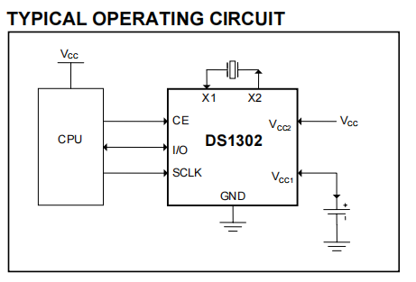
The working voltage range of DS1302 is 2V~5.5V. DS1302 controls and transmits data through only three lines: CE, I/O (Data line) and SCLK (Serial clock), as shown in the figure below. The read-write clock register or internal RAM (31 * 8-bit additional data temporary storage register) can adopt single byte mode and burst mode.
2. Working process
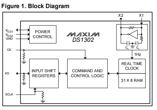
The working principle diagram is as follows, including shift register, control logic, crystal oscillator, clock and RAM. During any data transmission, CE must be set to high level (when CE is set to high level and the internal clock is still running under the action of crystal oscillator, external reading and writing of data is allowed). The data is input at the rising edge of each SCLK and output at the falling edge. Only one bit can be read and written at a time. Whether to read or write depends on the serial input control instruction, A byte can be read through 8 pulses, so as to realize serial input and output.
At the beginning, the control byte is loaded into the shift register through 8 clock cycles. If the control instruction is in single byte mode, 8 consecutive clock pulses can write 8-bit data and read 8-bit data. When the SCLK clock is on the rising edge, the data is written into DS1302. When the SCLK clock is on the falling edge, the data of DS1302 is read out, and 8 pulses can read and write a byte. In burst mode, 7-byte clock / calendar registers can be read and written at one time through continuous pulses, and 8 ~ 328 bit RAM data can also be read and written at one time (a certain number can be read and written according to the actual situation, without all reading and writing).
3. Control command
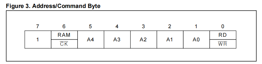
The transmission of each byte is specified by the control byte. The highest bit bit7 of the control byte must be 1. If it is' 0 ', writing will be prohibited. If this is 0, you can disable writing. bit6 is' 0 'to control the reading and writing operation of clock / calendar register, and' 1 'to control the reading and writing operation of RAM area data. bit1~bit5 specify the input and output operation of relevant registers, and the lowest bit 0 specifies whether to input or output. If it is' 0', it is write (input), and if it is' 1 ', it is read (output).
4. Data transmission
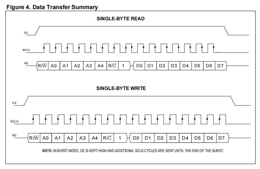
All data transmission is carried out when CE is set to 1. The CE input signal has two functions: first, CE turns on the control logic and allows the address / command sequence to be sent to the shift register; Second, CE provides a means to terminate the transmission of single byte or multi byte data. When CE is at high level, all data transmission is initialized, allowing operation of DS1302. If CE is set to low level during transmission, the data transmission will be terminated and the I/O pin will change to high resistance state. During power on operation, CE must be kept low before Vcc ≥ 2.5V. CE can be set to high level only when SCLK is low level. I/O is the serial data input / output terminal (bidirectional), and SCLK is always the input terminal. As shown in the figure, it is a sequence diagram of reading data and writing data.
(1) data input
After 8 clock cycles of control byte input, the input of one byte will be completed on the rising edge of 8 clock cycles, and the data transmission starts from the lowest byte.
(2) Data output
After the input of the control read instruction of 8 clock cycles, the data of one byte will be output on the falling edge of the next 8 clock cycles. Note that the first bit output is output on the falling edge of the pulse where the last bit control instruction is located, and CE is required to maintain high level.
Similarly, if the control read instruction of 8 clock cycles specifies the burst mode, the data will be read in at the rising edge of the pulse and read out at the falling edge. The burst mode can read and write multi byte data at one time, as long as the pulse is well controlled.
(3) Calendar clock register (data format: BCD code)
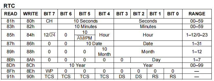
bit7 (CH) of the 1 ° sec register (80H and 81H) is the clock pause flag bit
When CH is 0, the clock oscillation stops;
When CH is 1, the clock starts running.
bit7 (WP) of the 2 ° control register (8EH and 8FH) is the write protect bit.
When WP is 0, any clock or RAM register can be written;
When WP is 1, writing to any register is prohibited.
2, Programming
/*******************Explain*****************

On the training platform, the time is displayed on the digital tube 1302

*/

#include "reg52.h"
#include "ds1302.h"
#include "SMG_show.h"


uchar write_ds1302_adrr[7] = {0x80,0x82,0x84,0x86,0x88,0x8a,0x8c};
uchar read_ds1302_adrr[7] = {0x81,0x83,0x85,0x87,0x89,0x8b,0x8d};
//Thursday, January 27, 22, 23:59:24 (BCD code)
uchar timer[7] = {0x24,0x59,0x23,0x27,0x01,0x04,0x22};


void ds1302_config()    //Initialize (enable) calendar clock
{
    uchar i;
    Write_Ds1302_Byte(0x8e,0x00);   //Turn off protection and start writing data (write protected, read unprotected)
    for(i = 0;i < 7;i++)
    {
        Write_Ds1302_Byte( write_ds1302_adrr[i],timer[i] );
    }
    Write_Ds1302_Byte(0x8e,0x80);   //Restore protection
}

void read_ds1302_timer()    //Get current time
{
    uchar i;
    for(i =0;i < 7;i++)
    {
        timer[i] = Read_Ds1302_Byte(read_ds1302_adrr[i]);   //Put the read data into the array

    }
}

void ds1302_show()
{
    SMG_show_bit(0,table_nodot[timer[2]/16]);    //Ten in an hour
    delay_ms(2);
    SMG_show_bit(1,table_nodot[timer[2]%16]);    //Bits per hour
    delay_ms(2);

    SMG_show_bit(2,0xbf);    //Display "-" 1011 1111
    delay_ms(2);

    SMG_show_bit(3,table_nodot[timer[1]/16]);    //Ten points
    delay_ms(2);
    SMG_show_bit(4,table_nodot[timer[1]%16]);    //Sub digit
    delay_ms(2);

    SMG_show_bit(5,0xbf);    //Display "-" 1011 1111
    delay_ms(2);

    SMG_show_bit(6,table_nodot[timer[0]/16]);    //Ten bits of a second
    delay_ms(2);
    SMG_show_bit(7,table_nodot[timer[0]%16]);    //Bits of seconds
    delay_ms(2);
}

void main()
{
    system_init();
    ds1302_config();
    while(1)
    {
        read_ds1302_timer();
        ds1302_show();
    }
}