What is serial communication
- Communication is divided into serial and parallel: serial refers to the communication with one line, and parallel refers to the communication with multiple lines at the same time.
- This kind of communication can also be called serial communication, serial communication, UART and USART.
- Features: asynchronous, serial, full duplex.
- Working mode: there are three lines (GND/RXD receiving line / TXD transmitting line); Data is processed in bytes in the CPU of the sender and receiver; Data is transmitted bit by bit on the communication line.
- Main concepts of serial communication: start bit, data bit, parity bit, stop bit and baud rate (the baud rate of the sender and receiver must be the same for how many bits are sent in one second)
- The serial communication function is provided by an internal peripheral of SOC, which has nothing to do with the CPU itself.
STC51 serial communication related register
Control registers PCON and SCON
Serial control register SCON: the serial control register SCON is used to select the working mode of serial communication and some control functions.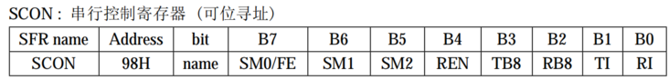
SM0/FE: when SMODO bit in PCON register is 1, this bit is used for frame error detection. When an invalid stop bit is detected, it is set through the UART receiver. It must be cleared by the software. When the SMODO bit in PCON register is 0, this bit and SM1 together specify the working mode of serial communication (SM0, SM1).
- 0: working mode 0; Synchronous shift serial mode; The baud rate is SYSclk/12
- 0 1: working mode 1; 8-bit UART with variable baud rate;
- 1 0: working mode 2; 9-bit UART;
- 1: working mode 3; 9-bit UART; Variable baud rate;
- REN: enable / disable serial reception control bit. (set and reset by software)
- TI: interrupt request flag bit when sending data. After sending a frame of data, the hardware will set automatically, that is, TI=1.
- RI: interrupt request flag bit when receiving data. After receiving a frame of data, the hardware will set automatically, i.e. RI=1.
Power control register PCON: used to select whether the baud rate is doubled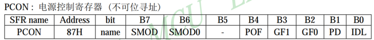
- SMOD: baud rate selection bit. SMOD=1, double; SMOD=0, not double.
- SMOD0: frame error detection effective control bit.
Interrupt enable register IE
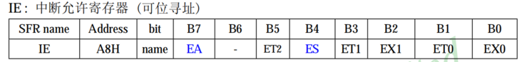
- EA: total interrupt allowed control bit of CPU.
- ES: serial port interrupt enable bit.
Timer / counter control register TCON
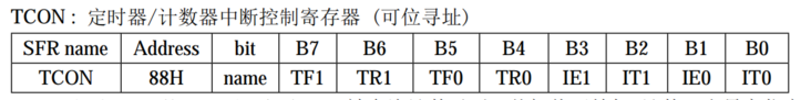
- TR1: operation control bit of timer T1. This bit is set and cleared by software.
- Start counting when TR1=1, and prohibit counting when TR1=0.
Serial port working mode
It mainly applies serial port working mode: 1:8-bit UART, with variable baud rate.
- When the software sets the SMO and SM1 of SCON to "01", the serial communication works in mode 1.
- A frame of information is 10 bits: 1 start bit, 8 data bits (low order first) and 1 stop bit.
- TXD is the sending information and RXD is the receiving information.
- After a frame of information is sent or received, an interrupt request will be initiated to set RI or TI.
Baud rate calculation formula
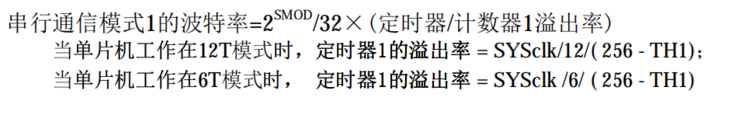
- SMOD is 0 or 1.
- SYSclk is the system clock frequency. (mine is 12MHz)
- TH1 is the automatic reload value. TH1 takes an integer.
be careful; When calculating the baud rate, the value of 256-TH1 must be in the position of a few zeros near the integer. Too much difference may cause garbled code. (if there is a difference of zero point 2, it may be garbled)
Code example
Serial port initialization
// Serial port initialization function
// Preset a serial port condition: 8 data bits, 1 stop bit, 0 check bit and 9600 baud rate
// The main work of initialization is to set the relevant registers
void uart_init(void)
{

    SCON = 0x50;       // 01010000 serial port works in mode 1 (8-bit serial port), and reception is allowed
    PCON = 0x00;        // Baud rate does not double

    // Settings related to communication baud rate
    TMOD = 0x20;        // As a timer, set T1 to mode 2 (8-bit automatic reload)
    TH1 = 243;            //2×12000000÷32÷12÷4800=13.0208,256-TH1=13,TH=243.
    TL1 = 243;           // 8-bit automatic reload. When overflow occurs, the value stored in TH1 will be automatically loaded into TL1. TH1 and TL1 must be the same

    TR1 = 1;                // Turn on T1 timer / counter
    ES = 1;                    //Serial port interrupt enable bit
    EA = 1;                    //Total interrupt allowed bit

}
send data
// The single chip microcomputer sends a byte to the computer through the serial port.
void uart_send_byte(unsigned char c)
{
   // Step 1, send a byte
   SBUF = c;

   // Step 2: first confirm that the serial port sending part is not busy
   while (!TI);

   // Step 3: the software resets the TI flag bit
   TI = 0;
}

//The single chip microcomputer sends characters to the computer
void uart_send_string(unsigned char *str)
{
    while (*str != '\0')
    {
        uart_send_byte(*str);        // Send 1 character
        str++;                        // The pointer points to the next character
    }
}


//The computer sends data to the single chip microcomputer, which receives the data and triggers the interrupt, RI=1.
void uart_isr(void) interrupt 4 using 1
{
    unsigned char tmp;

    if (RI)
    {
        tmp = SBUF;        // Reading SBUF is actually reading 1 byte received by the serial port
        RI = 0;
    }
    uart_send_byte(tmp); //Send the received data to the computer to test whether it is received successfully.
}
EEPROM of I2C communication based on 51 single chip microcomputer
Basic knowledge
- ROM (read only memory), RAM (random access memory), PROM (programmable ROM)
- EPROM (erasable ROM), EEPROM (electrically erasable ROM)
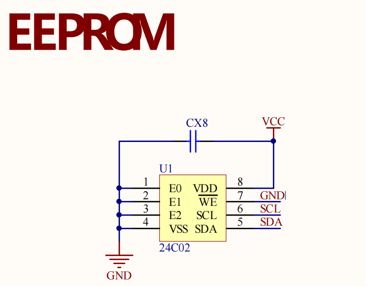
- The existence form of EEPROM in the system: built-in in the MCU or external expansion.
- EEPROM schematic diagram:
I2C bus protocol provisions
- Any device that transmits data to the bus is used as a transmitter, and any device that receives data from the bus is used as a receiver.
- The data transmission is controlled by the main device, and the serial clock, start and stop conditions of the bus are generated by the main device.
- Data transmission is allowed only when the bus is not busy.
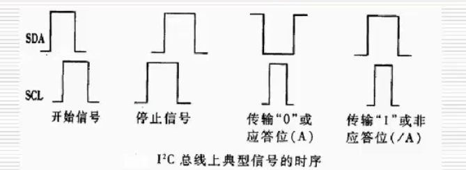
- During data transmission, when the clock line is at high level, the data line must be in a fixed state and no jump is allowed. When the clock line is high, any level change of the data line will be regarded as the start or stop condition of the bus.
- Start condition: the start condition must be sent before all operation commands. When the clock line remains high, the jump of the data line level from high to low is used as the start signal of I2C bus.
- Stop condition: when the clock line remains high, the jump of the data line from low to high is used as the stop signal of I2C bus. A stop condition must be sent at the end of the operation.
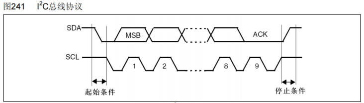
- I2C data transmission mode:
I2C summary
- The main CPU and its auxiliary chips are the most commonly used interfaces, especially various sensors.
- Three control lines: GND, SCL and SDA. Serial, level type. (the same is true in STM32 single chip microcomputer)
- Both sending and receiving bytes start from the high bit.
- The bus structure can be one to many, and hundreds of devices can be mounted on the bus, which can be distinguished by slave address.
- Master slave mode: the master device initiates communication and bus arbitration, and the slave device responds passively.
- The communication rate is low, which is not suitable for voice, video, etc.
I2C code example
/*******************************************************************************
* Function name: I2C_Start()
* Function: start signal: in I2C_SCL clock signal I2C during high level_ The SDA signal produces a falling edge
* Input: None
* Output: None
* Note: I2C after start_ SDA and I2C_SCL is 0
*******************************************************************************/

void I2C_Start()
{
    I2C_SDA = 1;
    I2C_Delay10us();
    I2C_SCL = 1;
    I2C_Delay10us();//The establishment time is I2C_SDA holding time > 4.7us
    I2C_SDA = 0;
    I2C_Delay10us();//The holding time is > 4us
    I2C_SCL = 0;
    I2C_Delay10us();
}
/*******************************************************************************
* Function name: I2C_Stop()
* Function: termination signal: in I2C_ I2C during SCL clock signal high level_ The SDA signal produces a rising edge
* Input: None
* Output: None
* Note: keep I2C after completion_ SDA and I2C_SCL is 1; Indicates that the bus is idle
*******************************************************************************/

void I2C_Stop()
{
    I2C_SDA = 0;
    I2C_Delay10us();
    I2C_SCL = 1;
    I2C_Delay10us();//The establishment time is greater than 4.7us
    I2C_SDA = 1;
    I2C_Delay10us();

}
/*******************************************************************************
* Function name: I2cSendByte(uchar num)
* Function: Send a byte through I2C. At I2C_ During SCL clock signal high level,
*                    * Keep sending signal I2C_SDA remains stable
* Input: num, ACK
* Output: 0 or 1. 1 is returned for sending success and 0 is returned for sending failure
* Note: after sending a byte I2C_SCL=0, if a response is required, the response is set to 1, otherwise it is 0
*******************************************************************************/

uchar I2C_SendByte(uchar dat, uchar ack)
{
    uchar a = 0,b = 0;//The maximum is 255, one machine cycle is 1us, and the maximum delay is 255us.
    // In order to ensure that the sequence is correct, SCL = 0 should be added here;
    for(a=0; a<8; a++)//To send 8 bits, start from the highest bit
    {
        I2C_SDA = dat >> 7;     //I2C after start signal_ SCL = 0, so I2C can be changed directly_ SDA signal
        dat = dat << 1;
        I2C_Delay10us();
        I2C_SCL = 1;
        I2C_Delay10us();//Establishment time > 4.7us
        I2C_SCL = 0;
        I2C_Delay10us();//Time greater than 4us
    }

    I2C_SDA = 1;            // The master device releases the SDA line to the slave device for operation
    I2C_Delay10us();
    I2C_SCL = 1;            // The main equipment starts the 9th cycle
    while(I2C_SDA && (ack == 1))//Wait for response, that is, wait for the slave device to send I2C_SDA pull down
    {
        b++;
        if(b > 200)     //If there is no reply over 200us, the transmission fails, or it is non reply, indicating that the reception is over
        {
            I2C_SCL = 0;
            I2C_Delay10us();
            return 0;
        }
    }

    I2C_SCL = 0;
    I2C_Delay10us();
     return 1;
}
/*******************************************************************************
* Function name: I2cReadByte()
* Function function: use I2c to read a byte
* Input: None
* Output: dat
* Note: after receiving a byte I2C_SCL=0
*******************************************************************************/

uchar I2C_ReadByte()
{
    uchar a = 0,dat = 0;
    I2C_SDA = 1;            //The CPU releases the bus and lets the slave take over. (it is handled in this way in 51 single chip microcomputer, which may be a little different in 32)
    I2C_Delay10us();
    // Logically, there should be a SCL = 0
    for(a=0; a<8; a++)//Receive 8 bits
    {
        I2C_SCL = 1;        // Inform the slave device that I want to start reading and can put 1 bit data into SDA
        I2C_Delay10us();
        dat <<= 1;            // When reading, it is high in front
        dat |= I2C_SDA;
        I2C_Delay10us();
        I2C_SCL = 0;        // Pull down to prepare for the next bit cycle
        I2C_Delay10us();
    }
    return dat;
}
EEPROM (Introduction to AT24C02 chip (255 bytes at most))
Device Addressing
- The master device starts the transmission process by sending a start signal, and then sends the slave device address. (slave address is defined by the chip itself)
- The upper 4 bits of the address of the 8-bit slave device are fixed as 1010, the next 3 bits are the address bits of the slave device, and the lowest bit is the read-write bit of the slave device (1 means to read and 0 means to write to the slave device)
- After the master device sends the start signal and the slave device address, AT24C02 will monitor the bus. When the address of a device is the same as the sent slave address, it will respond to a reply signal (through SDA line).
Response signal
- During I2C bus data transmission, the receiver must generate a response signal every time a byte of data is successfully transmitted. The receiver pulls the SDA down in the ninth clock cycle, indicating that a byte of data has been received.
- When AT24C02 works in the read state, it will release the bus after sending a byte and monitor the bus. If the response signal is received, it will continue to send data; If no response signal is received, stop sending data.
- Write operation sequence diagram) (ACK is the response signal)
Write operation
Write a single byte:
- First, the master device sends the start command and the slave device address information. Wait for a reply.
- Then send the memory address (i.e. byte address) to write data. Wait for a reply.
- Then start sending data. Wait for a reply.
- Finally, send a stop signal.
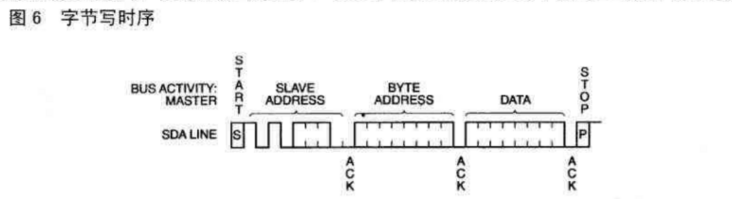
- Code example
/*******************************************************************************
* Function name: void At24c02Write(unsigned char addr,unsigned char dat)
* Function: write a data to an address of 24c02
* Input: None
* Output: None
*******************************************************************************/
void At24c02Write(unsigned char addr,unsigned char dat)
{
I2C_Start();
I2C_SendByte(0xa0, 1);//Send slave device address
I2C_SendByte(addr, 1);//Send address to write to memory
I2C_SendByte(dat, 0); //send data
I2C_Stop();
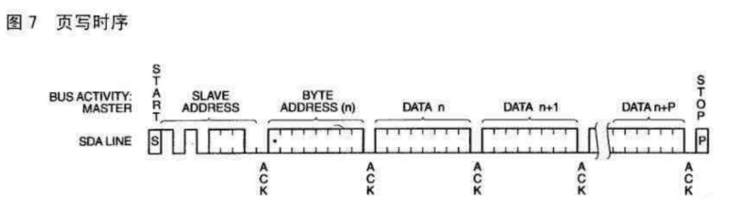
}Write multiple bytes continuously (AT24C01 can write 8 bytes at a time, and AT24C02/04/08/16 can write 16 bytes at a time)
- After each byte of data is sent, the AT24C chip will generate a response and add one to the low bit of the byte address, and the high bit remains unchanged.
- If the byte sent by the main device exceeds the specified byte before sending the stop signal, the exceeded byte will overwrite the previously written byte.
Read operation
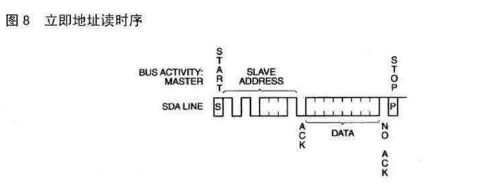
Immediate address read:
- If the address of the last read / write operation is n, the address read immediately starts from N+1. If the address limit is exceeded when reading data (AT04C02 can only save 255 bytes at most), it will flip to 0 address to continue reading.
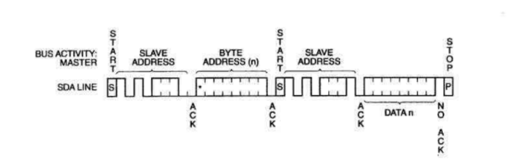
Selective reading:
- Selective read operation allows the main device to read any address of the register.
- Reading process: the master device first performs a pseudo write operation by sending the start signal, the slave device address and the byte data address to be read; After the response, the master device sends the start signal and the slave device address again. At this time, the last position of the address is one (read operation); AT24C02 responds and sends a response signal, and then sends the required data. The main device does not send a response signal, but sends a stop signal.
- Code example
/*******************************************************************************
* Function name: unsigned char At24c02Read(unsigned char addr)
* Function function: read a data of an address of 24c02
* Input: None
* Output: None
*******************************************************************************/

unsigned char At24c02Read(unsigned char addr)
{
    unsigned char num;
    I2C_Start();
    I2C_SendByte(0xa0, 1); //Send slave device address
    I2C_SendByte(addr, 1); //Send address to read
    I2C_Start();
    I2C_SendByte(0xa1, 1); //Send read device address
    num=I2C_ReadByte(); //Read data
    I2C_Stop();
    return num;
}