First of all, I would like to thank the bread board community< CPU Design practice - Wang Wenxiang and Xing Jinzhang read the preface after they got the book. They admired the author and his team for their contributions to the development of China core and trained batch after batch of computer talents for the country. In the preface, the book gave an overview and told readers that ordinary students can have it as long as they have systematic learning CPU Design capability. Here I am very excited and full of passion for reading this book. Next, let's explore it together CPU The mysterious world of design.
Chapter I overview of CPU chip R & D process
1 / 1 processor and processor core
At present, the common processor chips are no longer "arithmetic units" in the traditional sense+Controller ", but a system on chip( system on chip,SOC),That's the processor core SOC A core of IP.
A processor chip contains not only the processor core, but also advanced cache, high-speed bus interface controller and PHY,DDR3/4 Memory controller, etc.
Development process of 1 / 2 chip products
1,Definition of chip: in the chip definition stage, it is necessary to conduct market research, formulate the specification definition of chip according to customer needs, and conduct feasibility analysis and demonstration.
2,Chip design: the work in the chip design stage can be further divided into silicon chip design and packaging design.
3,Chip manufacturing: after the completion of silicon chip design and packaging design, it will be delivered to the factory and enter the chip manufacturing stage, including mask manufacturing, wafer production and packaging production.
4,Chip sealing test: after the chips pass the in-process test and completion test, ensure that these chips will not introduce errors in the production process, and then they can be finally verified.
5,Chip verification: the verification can be started only after the chip is welded to the circuit board, assembled into a machine and loaded with software. During the verification process, each technical index of the chip will be evaluated.
1 / 3 working stage of chip design
1. Clear design specifications
2. Formulate design scheme
3. Design description (writing RTL code)
4. Functional and performance verification
5. Logical synthesis
6. Layout planning
7. Layout and routing
8. Netlist logic verification, timing check and layout verification
9. Delivery film
Chapter 2 hardware experiment platform and FPGA design process
2 / 1 Hardware Experiment Platform
The FPGA uses XC7A200T-FBG676 of ARITEX-7 series.
2/2 FPGA design flow
1. Circuit design
2. Code writing
3. Functional simulation
4. Comprehensive implementation
5. On board commissioning
2 / 3 tasks and practices
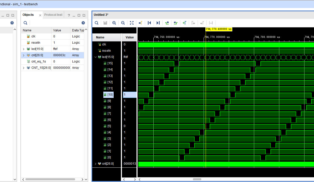
This task is to realize a running water lamp experiment. Since I don't have an experimental box, I can directly simulate and run it. Just look at the simulation diagram:
Chapter III design basis of digital logic circuit
3 / 1 digital logic circuit design and Verilog code development
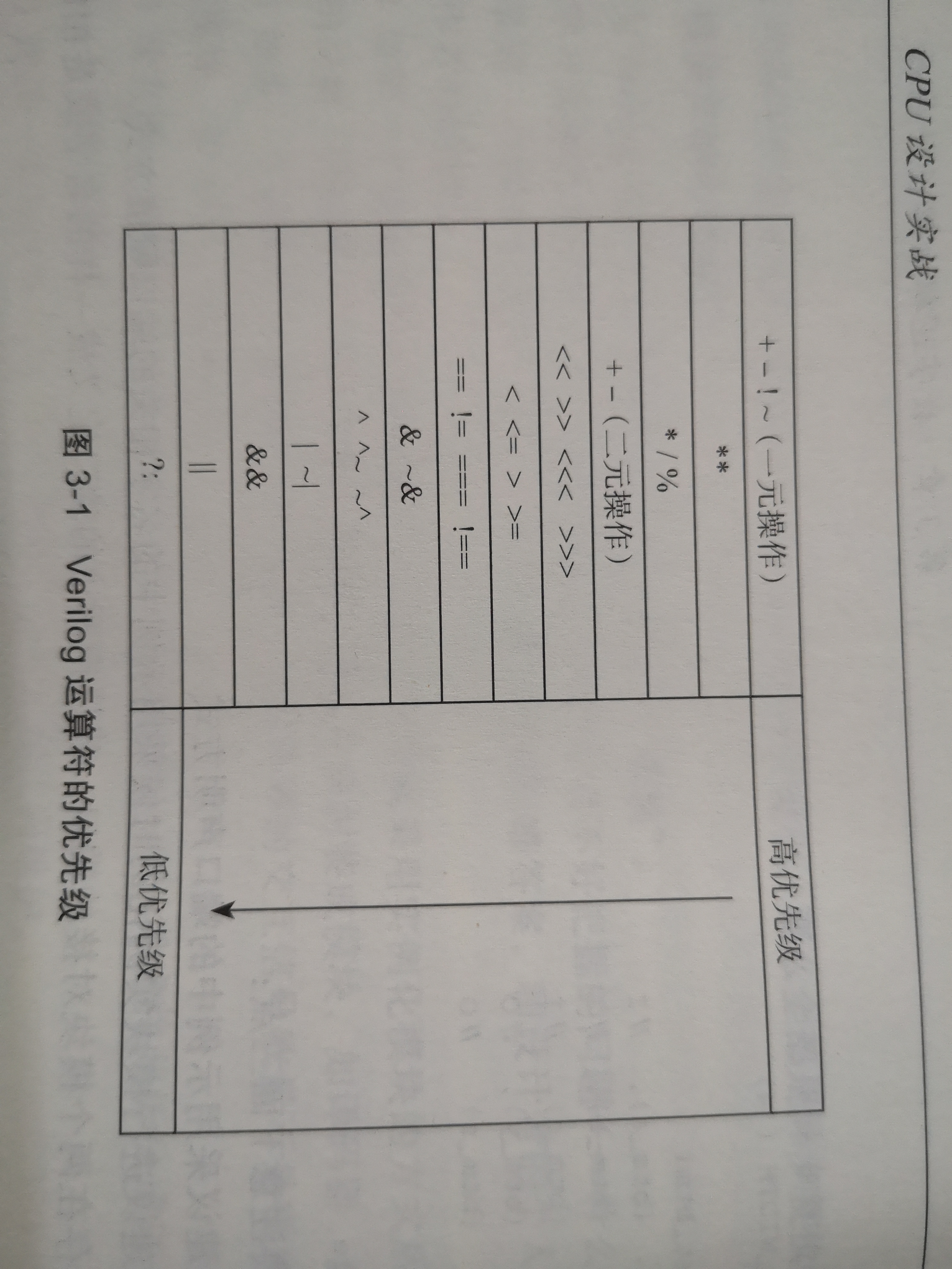
This summary mainly tells Verilog Language learning is combined with the design process of hardware digital circuit. You can read books here, such as hardware description language Verilog>,You can also find learning materials on various online platforms, such as rookie tutorials, blogs, etc. novices suggest learning basic grammar and keywords first, and then reading this book systematically will be more rewarding.
Highlights:
1,The core of hardware circuit oriented design thinking mode is actually "data path"( datapath)+Control logic( control logic)".
2,Behavior descriptive Verilog Programming style:
	[1]The advantages of behavior description (recommendation) are intuitive code expression, high coding efficiency and easy maintenance; [2] Circuit description;
3,Top-down design division process: "top-down, module division and layer by layer refinement". It is strongly recommended to consider the circuit structure design thoroughly before writing Verilog code.
4,Of common digital logic circuits Verilog Description:
	[1]Mandatory provisions
			1)Forbidden in code initial sentence.
			2)Forbidden in code casex,casez.
			3)Forbidden in code“#”Express current delay because it is not comprehensive.
			4)clock signal clock Only allowed in always @ (posedge clock)Statement.
			5)All triggers with reset in the code are either synchronous reset or asynchronous reset.
	[2]Module declaration and instantiation
			1)If a logic is used at least twice, and the logic adopts the method of instantiating modules, the readability of the code (number of code lines and code meaning) should be encapsulated into modules, such as decoders and multiplexers.
			2)If the functional specification of a logic is very clear and the number of interactive signals with the outside world is not very large, it should be encapsulated into modules, such as ALU,regfile Wait.
			3)The existing module has reached the scale of thousands of lines of code. You can consider splitting it into several small modules, such as one CPU It is divided into several modules according to the pipeline.
			4)It is recommended that only one module be included in a file for later code maintenance.
	[3]Basic logic gate
			When the code wants to identify a logical relationship, such as "condition" A1 Meet and conditions A2 Meet, or condition B "Satisfied", then use“&&"And“||";When the code wants to express logic gates, such as carry ahead generation logic of carry ahead adder and Wallace tree in multiplier, use“&"And“|".
	[4]Operator precedence
Later, in combination with the code, the reader also analyzes [5] decoder [6] encoder [7] multiplexer [8] ALU [9] trigger [10] register file [11] RAM [12] pipeline in simple MIPS CPU.
If you can understand the above examples and answer the questions in the book, it means that your Verilog language has been introduced. Ha ha.
Common errors and debugging methods of 3 / 2 digital logic circuit function simulation
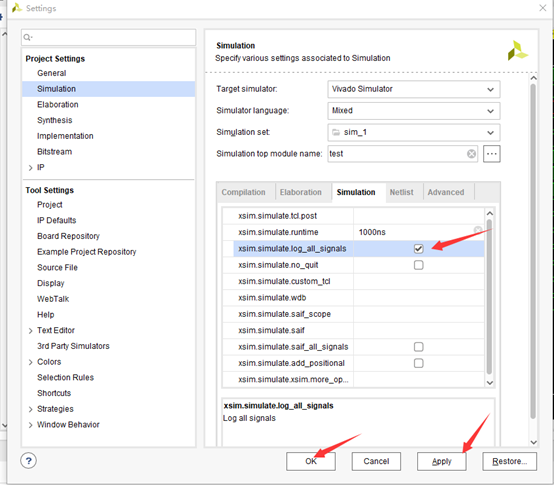
1,Function simulation waveform analysis
	[1]Idea of observing simulation waveform
			The first step is to get familiar with the design to be debugged (get familiar with your own design before debugging. If there is anything unclear, be sure to clarify the problem first, and sharpen the knife without mistaking the firewood cutter)
			The second step is to find a mistake you can identify (for complex problems) CPU,When there is an error in its function simulation, the output information usually does not directly tell you that the signal is wrong. You should learn the skill of locating the wrong point COU Design practice (Introduction)
			Finally, check the signal step by step backward along the designed logic chain until the source of the error is found (when observing the waveform containing sequential logic circuit, grab the clock signal used first, and clarify the timing devices to be checked, such as trigger and synchronization RAM Whether to trigger with the rising or falling edge of the clock, if it is traced all the way from the combinational logic to a trigger or RAM of Q On the end, it is necessary to grab all the non clock input signals of the trigger, then find the rising (falling) edge of the clock in which the error value is written forward along the time axis on the waveform, and then generate the trigger or RAM Continue to trace the input combinational logic, and be sure to find the error value written**real**Time)
	[2]Practical skills to improve the efficiency of waveform analysis
			1)Record the data of all signals in one simulation
			stay Vivado In the drawing view, click on the left“ PROJECT MANAGER"-"SETTINGS",Select in the pop-up setting interface“ Project Settings"-"simulation",Select the on the right“ simulation"Label and find it below“ xsim.simulate.log_all_signals"Check the option and click OK Save the configuration. In this way, all signals can be recorded in one simulation, and what signals need to be added.
2) Mark important moments
In the process of waveform analysis, you should mark the important moments in time.
3) Proficient in waveform reduction and amplification
4) Segmentation and grouping of correlated signals
"new divider" "new group"
5) Fast locating multi bit wide signal with value search
"find value"
2. Debugging of abnormal waveform errors (because the process is complex and analyzed according to the actual situation, only the title is described here)
[1] Signal is "Z"
[2] Signal is "X"
[3] Waveform stop
[4] Over edge sampling
[5] Weird waveform
3. Further use of Vivado
The summary involves the use of vivado software, which is not described here. If you are interested, you can find the use method of the software on the Internet or chat with me privately
[1] Custom synchronous RAM IP core
[2] Custom asynchronous RAM IP core
[3] View timing results and resource utilization
4. Experimental task
Chapter 4 simple pipeline CPU design
4 / 1 design a simple single cycle CPU
1,Design single cycle CPU General idea of
	[1]Instruction system specification
			Instruction system is the language system of computer hardware, also known as machine language. It is the interface between computer software and hardware, which can reflect the basic functions of computer.
			Instruction system specification is the specification file of instruction system. It gives a clear definition of each element in an instruction system.
			The specification document is attached at the back of this book C It is described in detail in.
	[2]CPU General design method of
			CPU Input, calculated, stored and output data flow on combinational logic circuits and sequential logic circuits. We often call these logic circuits**Data path**.
2,Single cycle CPU Path design
	[1]ADDU Instruction (the following are the data path components it needs)
			1)PC
			2)Virtual real address translation
				anytime CPU The addresses in the programs running on are virtual addresses, and CPU Memory accessed by itself IO The addresses used are physical addresses.
			3)instructions RAM
				After getting the physical address, send the address to memory. Here we RAM Further split into instructions RAM And data RAM Two physically independent RAM To simplify the design.
			4)Module division considerations
	[2]ADDIU instructions
	[3]SUBU
	[4]LW instructions
			1)Memory access address generation
			2)data RAM
			3)Register file writeback result selection
	[5]SW instructions
	[6]BEQ and BNE instructions
			1)Judge branching conditions
			2)Calculate jump target
			3)If you jump, modify the index PC Is the jump target, otherwise PC Plus 4 - i.e PC to update
	[7]JAL instructions
	[8]JR instructions
	[9]SLT and SLTU instructions
	[10]SLL,SRL and SRA instructions
			1)Input of shifter/output
			2)Internal implementation of shifter
	[11]LUI,AND,OR,XOR and NOR instructions
	[12]ALU
3,Single cycle CPU Control signal production
4,Reset processing
4 / 2 pipelined CPU design without considering related conflicts
1,Add pipeline inter level cache
	[1]Pipeline Division
	[2]Contents stored in pipeline cache
2,synchronization RAM Introduction of
3,Adjust update PC Data path
	[1]Adjust branch instruction update PC Data path
	[2]Adjust reset update PC Data path
4,Design of pipeline control signal without considering correlation conflict
4/3 CPU design and development environment (CPU_CDE)
1,Get started quickly CPU Design development environment
	[1]Decompression environment
	[2]Design your CPU
	[3]Integrate your CPU
	[4]Compile test program
	[5]Generate comparison Trace
	[6]myCPU simulation
	[7]myCPU Upper plate
	[8]myCPU debugging
	[9]MIPS-GCC Installation of cross compilation tool
2,CPU Organization and structure of design and development environment
	[1]Verify the computer hardware system used
	[2]Functional simulation verification
			1)be based on Trace Debugging aids for comparison
			2)Generation using reference model golden_trace
			3)use golden_trace monitor myCPU
	[3]func Program description
	[4]Compilation script description
	[5]Compilation result description
	[6]Loading of test program
	[7]Judgment of simulation verification results
	[8]FPGA Judgment of on-board verification results
3,CPU Advanced design and development environment
	[1]Upgrade works and IP nucleus
	[2]Re customization inst_ram
	[3]Regenerate gold_trace.txt
	[4]replace mif File fast simulation
4,CPU Functional simulation and debugging technology of design
	[1]Why based on Trace Debugging aids for comparison
			CPU The source of execution error may be passed far through the logical path of the test program before being found by the verifier. By this means, in most cases, the simulation verification platform can immediately report an error when the instruction at the source of the error has just been executed.
	[2]be based on trace Blind area of comparative debugging means and its countermeasures (mainly in the following three cases)
			1}	 myCPU Crash
			2)myCPU Execute an endless loop in which there are no instructions to write registers, such as "1: b 1b;nop"Such program fragments
			3)myCPU implement store Instruction error
			See books for specific countermeasures P-119
	[3]Learn to read assembler and disassembly code
			 This book briefly introduces some compilation knowledge,	In depth understanding of compilation related knowledge can be searched on the Internet.
	[4]CPU Signals to be captured during debugging and how to view these signals
	[5]Instruction correlation and pipeline conflict
	[6]Design of pipeline data forwarding
			This paper mainly describes the scheme and selection of forward data path design.