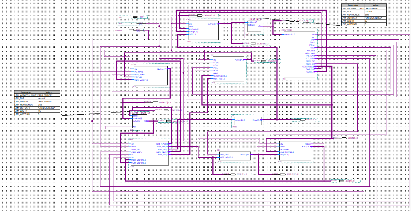
Experimental f4b 8-bit 12 instruction microprogram CPU design
- rom.mif
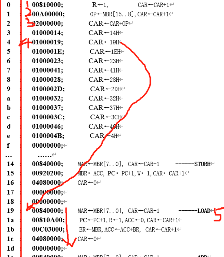
	0	:	00810000;        R←1,         CAR←CAR+1
	1	:	00A00000;       OP←MBR[15..8],CAR←CAR+1
	2	:	02000000;       CAR←CAR+OP
	3	:	01000014;       CAR←14H
	4	:	01000019;       CAR←19H
	5	:	0100001E;       CAR←1EH
	6	:	01000023;       CAR←23H
	7	:	01000041;       CAR←41H
	8	:	01000028;       CAR←28H
	9	:	0100002D;       CAR←2DH
	a	:	01000032;       CAR←32H
	b	:	01000037;       CAR←37H
	c	:	0100003C;       CAR←3CH
	d	:	01000046;       CAR←46H
	e	:	0100004B;       CAR←4H
	f	:	00000000;
   ...       ......
	14	:	00840000;    MAR←MBR[7..0], CAR←CAR+1     ------STORE
	15	:	00920200;    MBR←ACC, PC←PC+1,W←1,CAR←CAR+1
	16	:	04080000;    CAR←0
	17	:	00000000;
	18	:	00000000;
	19	:	00840000;    MAR←MBR[7..0], CAR←CAR+1      ------LOAD
	1a	:	00810A00;    PC←PC+1,R←1,ACC←0,CAR←CAR+1
	1b	:	00C03000;    BR←MBR,ACC←ACC+BR, CAR←CAR+1
	1c	:	04080000;    CAR←0
	1d	:	00000000;
	1e	:	00840000;    MAR←MBR[7..0], CAR←CAR+1  ----------ADD
	1f	:	00810200;    PC←PC+1,R←1,CAR←CAR+1
	20	:	00C03000;    BR←MBR,ACC←ACC+BR, CAR←CAR+1
	21	:	04080000;    CAR←0
	22	:	00000000;
	23	:	00840000;    MAR←MBR[7..0], CAR←CAR+1  ----------SUB
	24	:	00810200;    PC←PC+1,R←1,CAR←CAR+1
	25	:	00C04000;    BR←MBR,ACC←ACC-BR, CAR←CAR+1
	26	:	04080000;    CAR←0
	27	:	00000000;
	28	:	00840000;    MAR←MBR[7..0], CAR←CAR+1   ---------AND
	29	:	00810200;    PC←PC+1,R←1,CAR←CAR+1
	2a	:	00C06000;    BR←MBR,ACC←ACC AND BR,CAR←CAR+1
	2b	:	04080000;     CAR←0
	2c	:	00000000;
	2d	:	00840000;     MAR←MBR[7..0], CAR←CAR+1  ---------OR
	2e	:	00810200;     PC←PC+1,R←1,CAR←CAR+1
	2f	:	00C07000;     BR←MBR,ACC←ACC OR BR, CAR←CAR+1
	30	:	04080000;     CAR←0
	31	:	00000000;
	32	:	00840000;     MAR←MBR[7..0], CAR←CAR+1  ----------NOT
	33	:	00808200;     PC←PC+1, ACC←NOT ACC,CAR←CAR+1
	34	:	04080000;     CAR←0
	35	:	00000000;
	36	:	00000000;
	37	:	00840000;     MAR←MBR[7..0], CAR←CAR+1  ----------SHIFTR
	38	:	08092000;     PC←PC+1, ACC←SHIFT ACC to Right 1 bit,CAR←CAR+1
	39	:	04080000;     CAR←0
	3a	:	00000000;
	3b	:	00000000;
	3c	:	00840000;    MAR←MBR[7..0], CAR←CAR+1  -----------SHIFTL
	3d	:	0080A200;    PC←PC+1, ACC←SHIFT ACC to Left 1 bit,CAR←CAR+1
	3e	:	04080000;    CAR←0
	3f	:	00000000;
	40	:	00000000;
	41	:	00840000;    MAR←MBR[7..0], CAR←CAR+1  -----------JMPGEZ
	42	:	00805000;    CAR←CAR+1,
	43	:	04080000;    CAR←0
	44	:	00000000;
	45	:	00000000;
	46	:	00840000;    MAR←MBR[7..0], CAR←CAR+1  ------------MPY
	47	:	00810200;    PC←PC+1,R←1,CAR←CAR+1
	48	:	00C0B000;   BR←MBR,ACC←ACC*BR, CAR←CAR+1
	49	:	04080000;    CAR←0
	4a	:	00000000;
	4b	:	0100004B;    CAR←4BH  ------------------------------HALT
	4c	:	00000000;
-
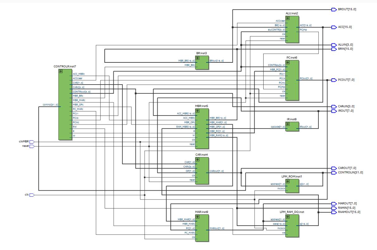
CPU circuit diagram
-
Simulation waveform of some operations
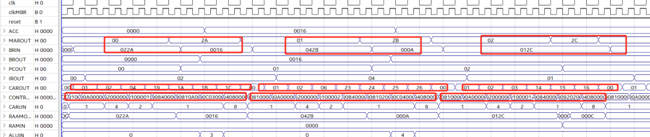
1, load, add, store, halt (22+10)
Contents in RAM:
0 : 022A; Load 2A
1 : 032B; ADD 2B
2 : 012C; Store 2C
3 : 0C00; Halt
2a : 0016;
2b : 000A;
The content of 2b addressing in RAM is 0020H
Operation waveform:
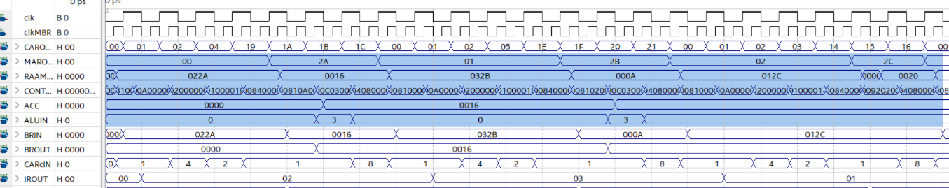
Program 1 waveform diagram, corresponding relationship analysis of data change one by one, instruction by instruction, stage by stage, operation by component, and data operation process analysis.
(for detailed analysis, any instruction can be selected as an example. Each flow and change of control signal, address, data and other information must be marked in combination with the specific description of test waveform, circuit diagram, code and instruction system design.)
At the beginning, the PC value is 0, and the PC passes the instruction address to MAR through the address bus.
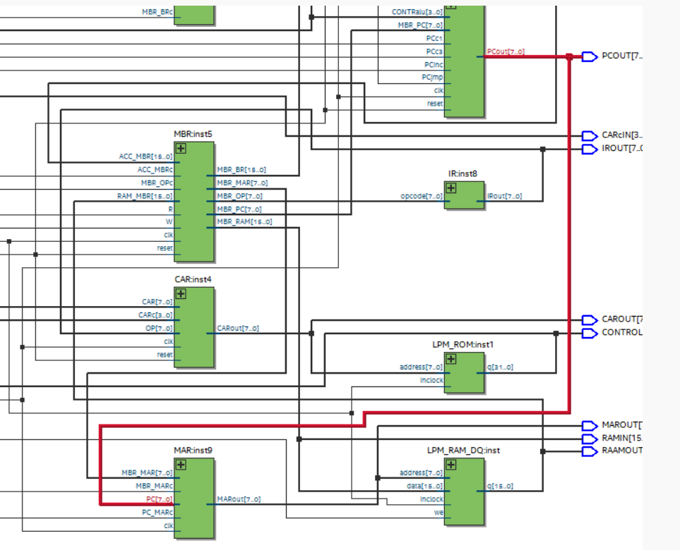
At the beginning, since the value of CAR is 0, then the value 0 in CAR will be passed in, and the corresponding micro instruction will be found in rom through the red line in the figure below.
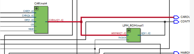
Then pass the microinstruction into the control through the red line data line in the figure below
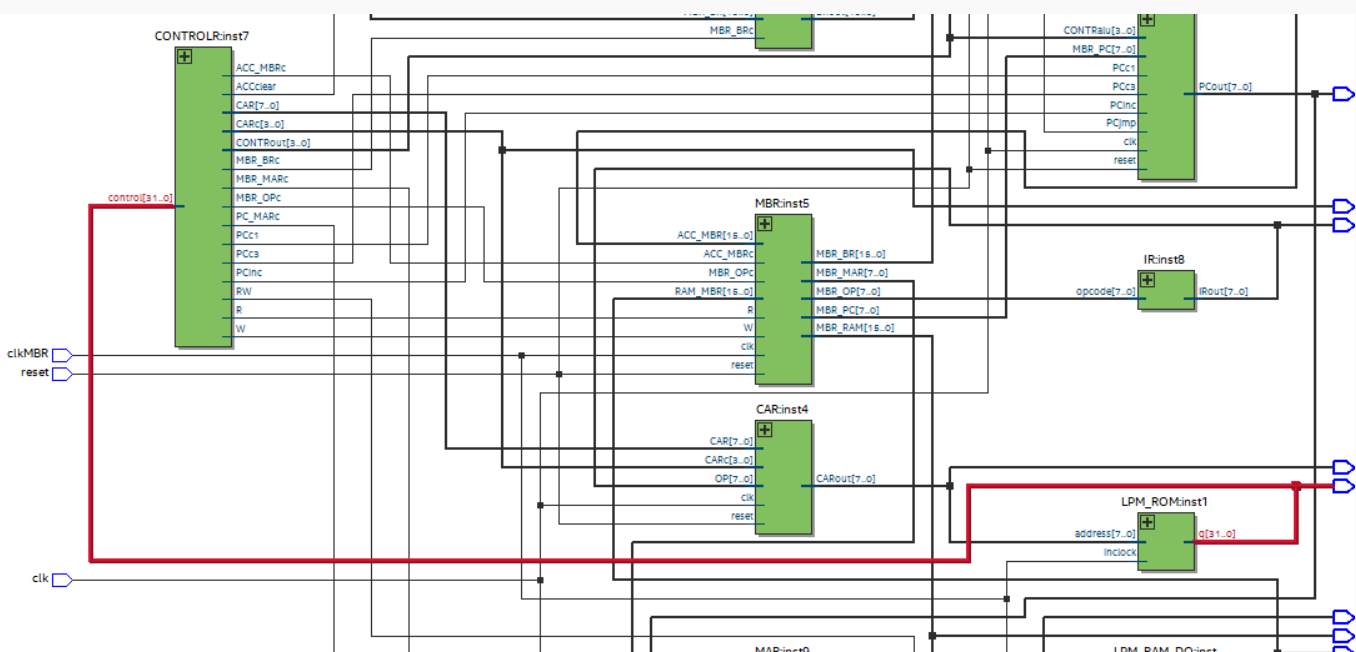
control obtains the instruction and transmits the signal to MAR
MAR takes instruction 022A from ram(0) through the red line in the figure below
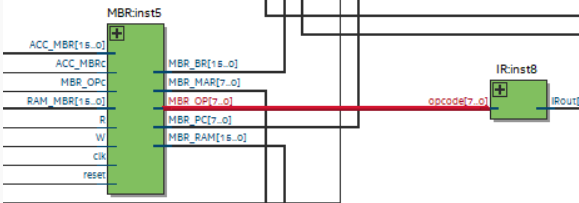
Then it is transmitted to MBR through the lower data bus, where 02 is the operation code and 2A is the address code
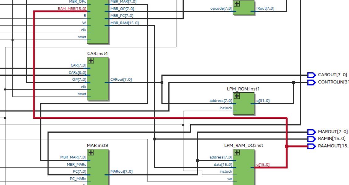
At this time, the CPU will set the read signal R to 1 and change the CAR value + 1 to 1. Then, it will pass the value 1 in the CAR to the rom as in the above process, find out the corresponding micro instruction, and pass the micro instruction to the control through the data line. Therefore, the CPU will read the operation codeword segment stored in the MBR, read it through the red line address bus in the figure below and store it in OP(IR), and change the CAR value + 1 to 1
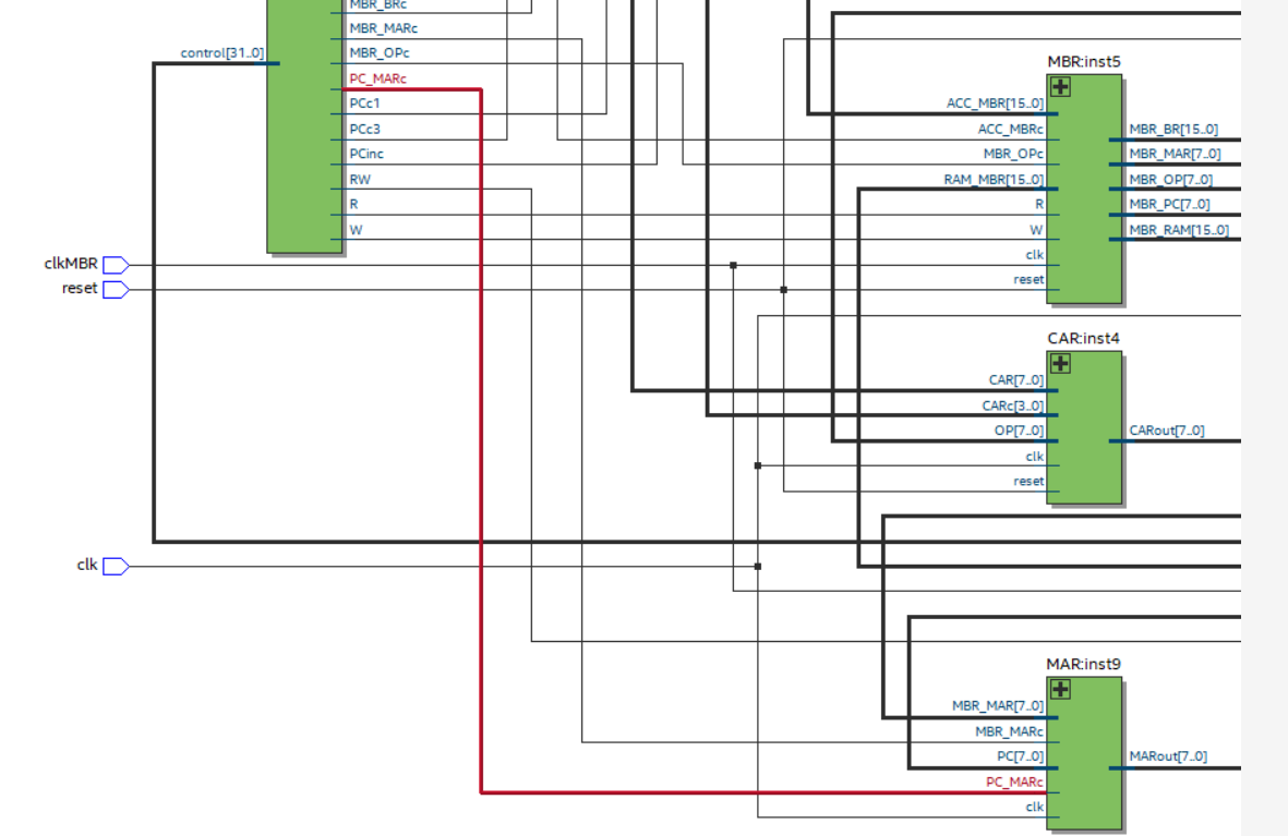
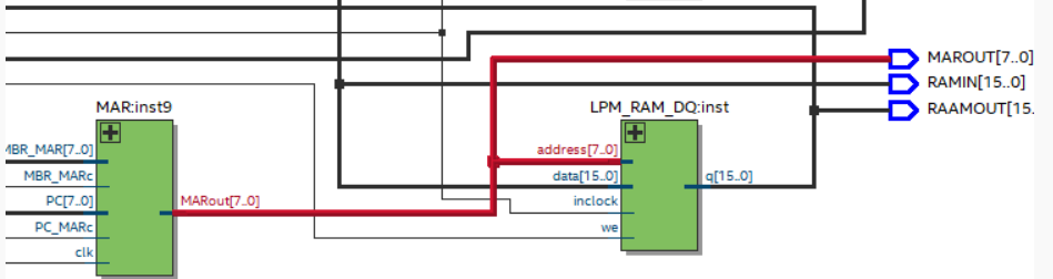
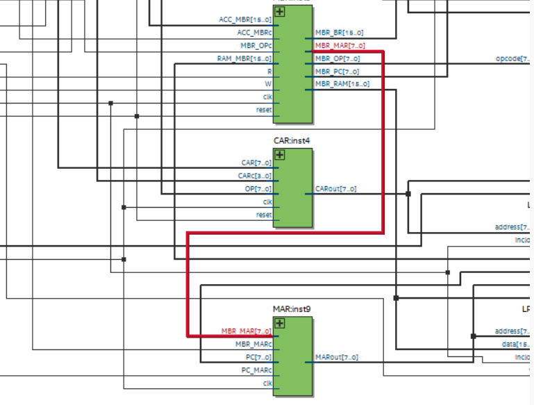
At this time, the value of CAR is 2, and then the value 2 in CAR will be passed into rom to find out the corresponding micro instruction, and the micro instruction will be passed into control through the data line. Therefore, the CPU will execute CAR ← CAR+OP operation to make the value of CAR change to 04; Then, the value 4 in the CAR will be passed into the rom to find the corresponding micro instruction, and the micro instruction will be passed into the control through the data line. At this time, the value of the CAR is 04, so the CPU will execute the CAR ← 19 to change the value of the CAR to 19; At this time, the value of CAR is 19, and then the value 19 in CAR will be passed into rom to find out the corresponding micro instruction, and the micro instruction will be passed into control through the data line. So far, the LOAD operation is officially entered. First, the address code in MBR will be passed into MAR through the red line address bus in the figure below
Then the value in ACC and the value in Br are added and coexisted back to ACC so that the ACC value is 16. Finally, the value of CAR will be + 1; At this time, the whole LOAD operation is completed, and the value of CAR is 1C. Then, the value 1c in CAR will be passed into rom to find out the corresponding micro instruction, and the micro instruction will be passed into control through the data line. The CPU will set the value in CAR to zero. Through the above operations, 0: 022a is completed; LOAD 2A this instruction. At this time, the PC value is 1, and the value in the PC will be transmitted to MAR through the address bus. Then, the instruction 032B is taken out from ram(1) and transmitted to MBR through the data bus, where 03 is the operation code and 2b is the address code. At the beginning, since the value of CAR is 0, then the value 0 in CAR will be passed into rom to find out the corresponding micro instruction, and the micro instruction will be passed into control through the data line. At this time, the CPU will set the read signal R to 1 and change the value of CAR + 1 to 1; At this time, the value of the CAR is 1, and then the value 1 in the CAR will be passed into the rom to find the corresponding micro instruction, and the micro instruction will be passed into the control through the data line. Therefore, the CPU will read the opcode field stored in the MBR, read it through the address bus and store it in the OP, and change the value of the CAR + 1 to 1; At this time, the value of CAR is 2, and then the value 2 in CAR will be passed into rom to find out the corresponding micro instruction, and the micro instruction will be passed into control through the data line. Therefore, the CPU will execute CAR ← CAR+OP operation to make the value of CAR become 05; At this time, the value of CAR is 05, and then the value 5 in the CAR will be passed into the rom to find the corresponding micro instruction, and the micro instruction will be passed into the control through the data line. Therefore, the CPU will execute CAR ← 1E to change the value of CAR to 1e; At this time, the value of the CAR is 1E, and then the value 1E in the CAR will be passed into the rom to find the corresponding micro instruction, and the micro instruction will be passed into the control through the data line. At this point, the ADD operation will be officially entered. First, the address code in the MBR will be passed into the MAR through the address bus, and then the value of the CAR + 1; At this time, the value of the CAR is 1f, and then the value 1F in the CAR will be passed into the rom to find the corresponding micro instruction, and the micro instruction will be passed into the control through the data line. At this time, the CPU will execute the operation of PC+1, set the read signal R to 1, and finally ADD the value of the CAR to 1; At this time, the value of the CAR is 20, then the value 20 in the CAR will be passed into the rom to find the corresponding micro instruction, and the micro instruction will be passed into the control through the data line. The CPU will pass the operand 000A corresponding to the operation code in the MBR into the br through the data bus, and then the value in ACC and the value in BR will be added and coexisted back to ACC, so that the ACC value is 0020, and finally the value of the CAR will be + 1; At this time, the whole ADD operation is completed, the value of the CAR is 21, and then the value 21 in the CAR will be passed into the rom to find out the corresponding micro instruction, and the micro instruction will be passed into the control through the data line, and the CPU will set the value in the CAR to zero.
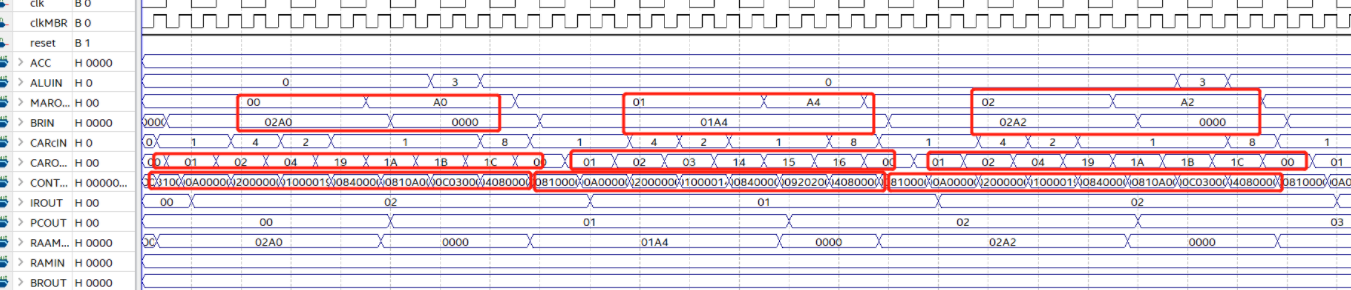
2, load, SUB, store, halt (22-10)
The contents in RAM:
0 : 022A; Load 2A
1 : 042B; SUB 2B
2 : 012C; Store 2C
3 : 0C00; Halt
2a : 0016;
2b : 000A;
The content in RAM addressed of 2c is 000C(H).
The waveform of the operate:
The operation process of the instruction is basically the same as the addition instruction above. The difference is that the opcode OP of 042B is 04 and 02 on the CAR is 06. At this time, the value of the CAR is 06, and then the value 6 in the CAR will be passed into the rom to find out the corresponding micro instruction, and the micro instruction will be passed into the control through the data line. Therefore, the CPU will execute CAR ← 23 to change the value of the CAR to 23; At this time, the value of the CAR is 23, and then the value 23 in the CAR will be passed into the rom to find the corresponding micro instruction, and the micro instruction will be passed into the control through the data line. At this point, the SUB operation will be officially entered. First, the address code in the MBR will be passed into the MAR through the address bus, and then the value of the CAR + 1; At this time, the value of the CAR is 24, and then the value 24 in the CAR will be passed into the rom to find the corresponding micro instruction, and the micro instruction will be passed into the control through the data line. At this time, the CPU will execute the operation of PC+1, set the read signal R to 1, and finally add the value of the CAR to 1; At this time, the value of CAR is 25, the CPU will transfer the operand 000A corresponding to the operation code in MBR to br through the data bus, and then the value in ACC and the value in BR will be subtracted and coexisted back to ACC, so that the ACC value is 000C, and finally the value of CAR will be + 1; At this time, the whole SUB operation is completed, the value of CAR is 26, and then the value 26 in CAR will be passed into rom to find out the corresponding micro instruction, and the micro instruction will be passed into control through the data line, and the CPU will set the value in CAR to zero.
3, Sum from 1 to 100
The contents in RAM are shown in table2.
The content in RAM addressed of A4 is 13BA(H).
The waveform of the operate:
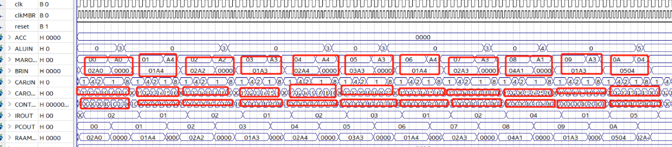
The clock cycle of CAR is 400 ns.
From the waveform, it takes 2.314ms to execute the operate. So the number of the executing cycles is 2.134/0.0004=5335.
Program 4 waveform diagram, corresponding relationship analysis of data change one by one, instruction by instruction, stage by stage, operation by component, and data operation process analysis. (required)
Take the ADD A3 instruction of the first cycle as an example. At this time, the PC value is 05. The PC value is transmitted to MAR through the address bus, and then the instruction 03A3 is taken out of ram and transmitted to MBR through the data bus. At the beginning, since the value of CAR is 0, then the value 0 in CAR will be passed into rom to find out the corresponding micro instruction, and the micro instruction will be passed into control through the data line. At this time, the CPU will set the read signal R to 1 and change the value of CAR + 1 to 1; At this time, the value of the CAR is 1, and then the value 1 in the CAR will be passed into the rom to find the corresponding micro instruction, and the micro instruction will be passed into the control through the data line. Therefore, the CPU will read the opcode field stored in the MBR, read it through the address bus and store it in the OP, and change the value of the CAR + 1 to 1; At this time, the value of CAR is 2, and then the value 2 in CAR will be passed into rom to find out the corresponding micro instruction, and the micro instruction will be passed into control, so the CPU will execute CAR ← CAR+OP operation, so that the value of CAR becomes 05; At this time, the value of CAR is 05, and then the value 5 in the CAR will be passed into the rom to find the corresponding micro instruction, and the micro instruction will be passed into the control through the data line. Therefore, the CPU will execute CAR ← 1E to change the value of CAR to 1e; At this time, the value of the CAR is 1E, and then the value 1E in the CAR will be passed into the rom to find the corresponding micro instruction, and the micro instruction will be passed into the control through the data line. At this point, the ADD operation will be officially entered. First, the address code in the MBR will be passed into the MAR through the address bus, and then the value of the CAR + 1; At this time, the value of the CAR is 1f, and then the value 1F in the CAR will be passed into the rom to find the corresponding micro instruction, and the micro instruction will be passed into the control through the data line. At this time, the CPU will execute the operation of PC+1, set the read signal R to 1, and finally ADD the value of the CAR to 1; At this time, the value of CAR is 20, then the value 20 in CAR will be passed into rom to find out the corresponding micro instruction, and the micro instruction will be passed into control through the data line. The CPU will pass the operand 0064 corresponding to the operation code in MBR into br through the data bus, and then the value in ACC and the value in BR will be added and coexisted back to ACC, so that the ACC value is 0064, and finally the value of CAR will be + 1; At this time, the whole ADD operation is completed, the value of the CAR is 21, and then the value 21 in the CAR will be passed into the rom to find out the corresponding micro instruction, and the micro instruction will be passed into the control through the data line, and the CPU will set the value in the CAR to zero.
-
(I)The GDF of CPU:
-
(II) The code of the CPU program:
1, MBR     (Memory Buffer Register)

library ieee;

use ieee.std_logic_1164.all;

use ieee.std_logic_unsigned.all;

entity MBR is

port( clk, reset, MBR_OPc, ACC_MBRc,R,W:in std_logic;

     ACC_MBR :in std_logic_vector(15 downto 0);

     RAM_MBR :in std_logic_vector(15 downto 0);

     MBR_RAM :out std_logic_vector(15 downto 0);

     MBR_BR  :out std_logic_vector(15 downto 0);

     MBR_OP  :out std_logic_vector(7 downto 0);

     MBR_MAR :out std_logic_vector(7 downto 0);

     MBR_PC  :out std_logic_vector(7 downto 0));

end MBR;

architecture behave of MBR is

begin

  process(clk)

  variable temp:std_logic_vector(15 downto 0);

  begin

    if(clk'event and clk='0')then

     if reset='1' then

       if ACC_MBRc='1' then  temp:=ACC_MBR;   end if;

       if R='1' then    MBR_BR<=RAM_MBR;     end if;

       if W='1' then      MBR_RAM<=temp;      end if;

       MBR_MAR<=RAM_MBR(7 downto 0);

       MBR_PC<=RAM_MBR(7 downto 0);

       if MBR_OPc='1' then   MBR_OP<=RAM_MBR(15 downto 8);    end if;

      else MBR_BR<=x"0000";

           MBR_MAR<="00000000";

           MBR_OP<="00000000";

           MBR_PC<="00000000";

      end if;

    end if;

  end process;

end behave;


2, BR         (Buffer Register)

library ieee;

use ieee.std_logic_1164.all;


entity BR is

port( MBR_BRc:in std_logic;

     MBR_BR:in std_logic_vector(15 downto 0);

     BRout:out std_logic_vector(15 downto 0));

end BR;

architecture behave of BR is

begin

  process

  begin

       if MBR_BRc='1' then     BRout<=MBR_BR;     end if;

  end process;

end behave;


3,  MAR      (Memory Address Register)

library ieee;

use ieee.std_logic_1164.all;

use ieee.std_logic_unsigned.all;

entity MAR is

port( clk,PC_MARc,MBR_MARc:in std_logic;

     PC,MBR_MAR:in std_logic_vector(7 downto 0);

     MARout:out std_logic_vector(7 downto 0));

end MAR;

architecture behave of MAR is

begin

  process(clk)

  begin

    if(clk'event and clk='1')then

       if PC_MARc='1' then      MARout<=PC;           end if;

       if MBR_MARc='1' then    MARout<=MBR_MAR;   end if;

    end if;

  end process;

end behave;


4, PC         (Program Counter)

library ieee;

use ieee.std_logic_1164.all;

use ieee.std_logic_unsigned.all;

entity PC is

port( clk,PCjmp,PCc1,PCinc,PCc3,reset:in std_logic;

     CONTRalu  :in std_logic_vector(3 downto 0);

     MBR_PC   :in std_logic_vector(7 downto 0);

     PCout      :buffer std_logic_vector(7 downto 0));

end PC;

architecture behave of PC is

begin

  process(clk)

  begin

    if(clk'event and clk='0')then

      if reset='1' then

         if CONTRalu="0101" then

           if PCjmp='1' then            PCout<=MBR_PC;

            elsif PCjmp='0' then PCout<=PCout+1;

           end if;

         end if;

         if PCc1='1' then          PCout<="00000000";       end if;

         if PCinc='1' then          PCout<=PCout+1;         end if;

         if PCc3='1' then          PCout<=MBR_PC;         end if;

      else PCout<="00000000";

      end if;

    end if;

  end process;

end behave;


5, IR          (Instruction Register)

library ieee;

use ieee.std_logic_1164.all;

use ieee.std_logic_unsigned.all;

entity IR is

port( opcode  :in std_logic_vector(7 downto 0);

     IRout   :out std_logic_vector(7 downto 0));

end IR;

architecture behave of IR is

begin

    IRout<=opcode;

end behave;


6, CAR        (Control Address Register)

library ieee;

use ieee.std_logic_1164.all;

use ieee.std_logic_unsigned.all;

entity CAR is

port( clk,reset :in std_logic;

     CARc  :in std_logic_vector(3 downto 0);

     CAR,OP   :in std_logic_vector(7 downto 0);

     CARout:buffer std_logic_vector(7 downto 0));

end CAR;

architecture behave of CAR is

begin

  process(clk)

  begin

    if(clk'event and clk='1')then

     if reset='1' then

      if CARc="1000" then         CARout<="00000000";       end if;

      if CARc="0100" then         CARout<=OP+CARout;      end if;

      if CARc="0010" then       CARout<=CAR;              end if;

      if CARc="0001" then       CARout<=CARout+1;         end if;

     else CARout<="00000000";

     end if;

    end if;

 end process;

end behave;


7, CONTRALR   (Control Buffer Register)

library ieee;

use ieee.std_logic_1164.all;

use ieee.std_logic_unsigned.all;

entity CONTROLR is

port(

     control :in std_logic_vector(31 downto 0);

     R,W, RW, PCc1,PCinc,PCc3:out std_logic;

     ACCclear,MBR_MARc,PC_MARc:out std_logic;

     ACC_MBRc,MBR_OPc,MBR_BRc:out std_logic;

     CONTRout:out std_logic_vector(3 downto 0);

     CARc  :out std_logic_vector(3 downto 0);

     CAR   :out std_logic_vector(7 downto 0));

end CONTROLR;

architecture behave of CONTROLR is

begin

  process

  begin

       CAR<=control(7 downto 0);

       PCc1<=control(8);

       PCinc<=control(9);

       PCc3<=control(10);

       ACCclear<=control(11);

       CONTRout<=control(15 downto 12);

       R<=control(16);

       W<=control(17);

       MBR_MARc<=control(18);

       PC_MARc<=control(19);

       ACC_MBRc<=control(20);

       MBR_OPc<=control(21);

       MBR_BRc<=control(22);

       CARc<=control(26 downto 23);

       RW<=control(17);

end process;

end behave;


8, ALU        (Arithmetic Logic Unit)

library ieee;

use ieee.std_logic_1164.all;

use ieee.std_logic_unsigned.all;

entity ALU is

port( clk,reset,ACCclear:in std_logic;

     aluCONTR :in std_logic_vector(3 downto 0);

     BR       :in std_logic_vector(15 downto 0);

     PCjmp    :out std_logic;

     ACC      :buffer std_logic_vector(15 downto 0));

end ALU;

architecture behave of ALU is

begin

  process(clk)

  begin

    if(clk'event and clk='0')then

     if reset='0' then ACC<=x"0000";

      else

       if ACCclear='1' then        ACC<=x"0000";       end if;

       if aluCONTR="0011" then   ACC<=BR+ACC;      end if;      --ADD

       if aluCONTR="0100" then   ACC<=ACC-BR;       end if;      --SUB

       if aluCONTR="0110" then   ACC<=ACC and BR;   end if;      --AND

       if aluCONTR="0111" then   ACC<=ACC or BR;    end if;       --OR

       if aluCONTR="1000" then   ACC<=not ACC;      end if;       --NOT

       if aluCONTR="1001" then                                   --SRR

          ACC(14 downto 0)<=ACC(15 downto 1);    ACC(15)<='0';

       end if;

       if aluCONTR="1010" then                                   --SRL

          ACC(15 downto 1)<=ACC(14 downto 0);     ACC(0)<='0';

       end if;

       if aluCONTR="1011" then   ACC<=ACC*BR;       end if;     --MPY

      end if;

     end if;

     if ACC>0 then         PCjmp<='1';

         else PCjmp<='0';

     end if;

  end process;

end behave;