I. Experimental Contents
To realize Cache and its address transformation logic (also called Cache controller), the CPU reads data from Cache by directly connected address transformation. If it cannot read, it must consider reading data from main memory first, then writing data to Cache, and then sending data to CPU; secondly, the CPU writes data to memory.
Description: CLK is the system clock (used for counter counting control, etc.), CLR is the total clearing signal (clearing table memory, counter), WCT is the memory signal of writing Cache table, AB31.AB0 is the address bus of CPU accessing memory, 32-bit data is DB31.DB0 (data bus), RD (0, read) is the read signal of Cache, MWr (1, write) is the main one. Memory write signal, MRd (0, read) is the main memory read signal, M (1, valid, hit) is the Cache effective bit sign signal (area table memory mark), CA17. CA0 is the Cache address, MD31. MD0 is the main memory to send Cache data, D31. D0 is the Cache to send CPU data, LA3. LA0 is the intrablock address.
II. Experimental Principles
The address transformation used in this experiment is a direct association mapping method, which is simple and direct. The hardware implementation is simple, and the access speed is relatively fast, but the block conflict rate is relatively high. The main principle is that a block in main memory can only be mapped to a specific block in Cache.
Assuming that the block number of main memory is B and that of Cache is b, the mapping relationship between them can be expressed as follows:
b = B mod Cb
Cb is the block capacity of Cache. If the block capacity of main memory is Mb and the area capacity is Me, the relationship between direct mapping methods is shown in Figure 1. Main memory is divided into partitions according to the size of Cache. Generally, the capacity of main memory is an integral multiple of the capacity of Cache. The number of blocks in each partition of main memory is equal to the total number of blocks in Cache. Direct mapping can only map those blocks with the same block number in each main memory area to the specific block with the same block number in Cache. For example, Block 0 of main memory can only be mapped to block 0 of Cache, block 1 of main memory can only be mapped to block 1 of Cache. Similarly, block Cb of main memory 1 (the relative block number in block 1 is 0) can only be mapped to block 0 of Cache, as shown in Figure 1. According to the address mapping rule given above, the whole Cache address is identical to the lower part of the main memory address.
| Figure 1: Direct Connection 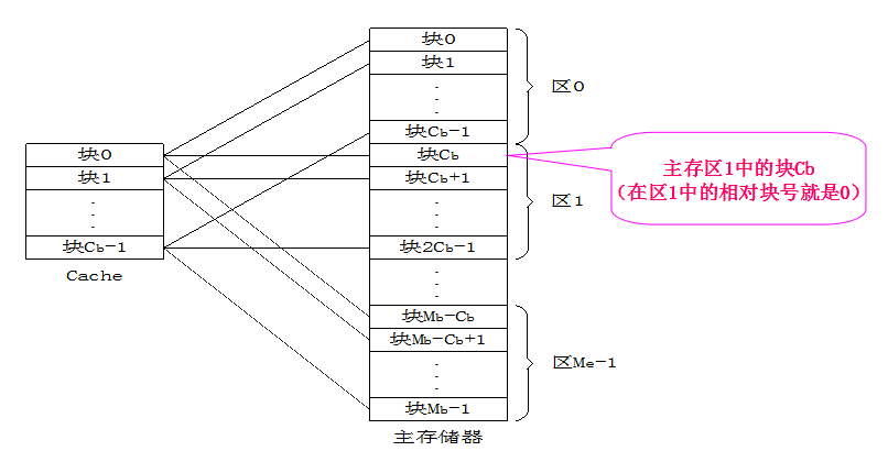
The process of address transformation in direct mapping is shown in Figure 2. The main memory address is divided into three parts: area number E, block number B and block address W. The Cache address is divided into two parts: block number B and block address W. Block number B in main memory address is exactly the same as block number B in Cache address. Similarly, the intra-block address W in the main memory address is exactly the same as the intra-block address w in the Cache address. The part where the main memory address is longer than the Cache address is called the area code E.
| Figure 2: Diagram of Direct Associated Address Transform 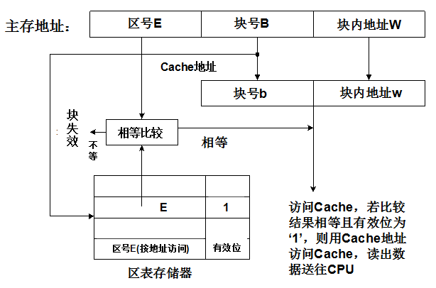
In the process of program execution, when accessing Cache, in order to realize the conversion from main memory block number to Cache block number, a small capacity memory (called area table memory) is needed to store the main memory area number. The capacity of this memory is equal to the number of blocks of Cache, and the word length is the length of area number E in the main memory address, plus a valid bit (hit/failure).
In the process of conversion from main memory address to Cache address, the block number B in the main memory address is used to access the area table memory (using block number B as the address of the area table memory to access it), and then the read area number is compared with the area number E in the main memory address. The result of comparison is equal. If the effective bit is 1, the Cache hits, indicating that the block to be accessed has been loaded into Cache. If the comparison results are not equal, the effective bit is 1, which can be replaced, and if the effective bit is 0, the required block can be directly transferred. As for the relatively unequal situation, whether the effective bit is 1 or 0, Cache has not hit, or is called Cache failure, which means that the block to be accessed has not been loaded into Cache. At this time, the main memory address is used to access the main memory. First, the block where the address is located is read into Cache, and then the data of the address in Cache is read and sent to CPU.
The relationship between Cache and CPU and memory is shown in the following figure.
| Figure 3: Basic framework of Cache 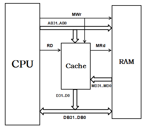
As shown in Figure 3, 32-bit main memory address is AB31.AB0 (address bus), 32-bit data is DB31.DB0 (data bus), RD (0, read) is the read signal of Cache, MWr (1, write) is the write signal of main memory, MRd (0, read) is the read signal of main memory, D31.D0 is the data signal sent by Cache to CPU (through a three-state buffer at the exit and then output), MD31.M. D0 is the data signal sent to Cache by RAM.
As shown in Figure 4, the area number E is 14 bits, the block number B is 14 bits, and the intra-block address is 4 bits, so the Cache address is 18 bits, of which the Cache block number B is 14 bits and the intra-block address w is 4 bits, so the capacity of Cache is 256 KB (2 ^ 18) units and the block number B is 14 bits. Then the Cache is divided into 16 KB (2 ^ 14) blocks and the intra block address w is 4 bits, and each block is 16 units (one byte per unit).
| Figure 4 Address Segmentation Diagram 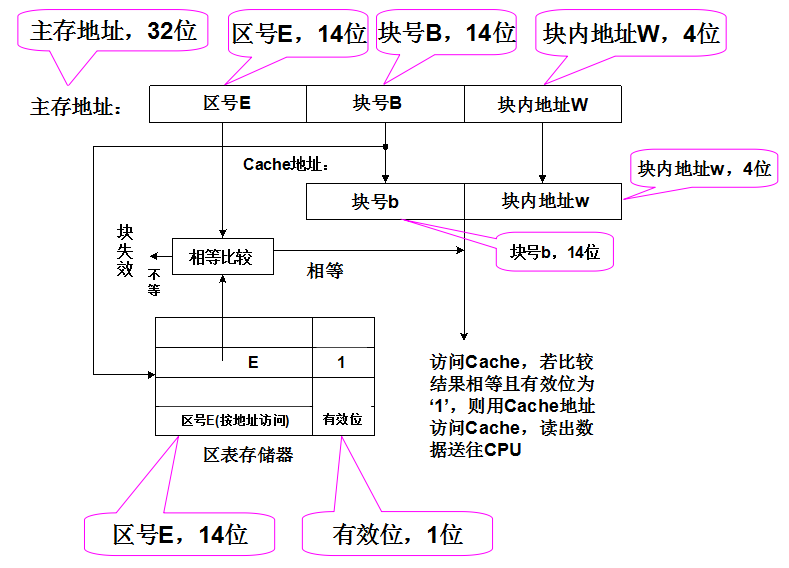
The way to implement Cache's memory is to first implement an 8-bit storage unit, and then use this 8-bit storage unit to construct a 256 Kb X 8-bit Cache (address 18 bits).
A 15-bit (14+1) storage unit is implemented, and then a 16kX 15-bit area table memory (14-bit address is the same as block number B) is constructed with this 15-bit storage unit, which is used to store area number (14-bit) and effective bit M(1-bit). In this part, we also need to implement an area code E comparator, that is, if the area number E of the main memory address is equal to the area number E of the corresponding unit taken out by the block number B as the address in the area table memory, the effective bit sign is M, and the effective bit M=1, then the Cache hits, otherwise the Cache fails, and the M=0 indicates the Cache fails.
When a Cache hits, it sends the data of the corresponding unit in the Cache storage to the CPU, which is a relatively simple process. When Cache fails, the data in the corresponding block in main memory is read out and written into Cache, so the Cache controller generates the read signal MRd (0, read) of the main memory. Since each block of Cache occupies 16 units and is accessed by 32 bits (4 bytes), it is necessary to access the main memory four times continuously, read the data of the block in the memory, that is, 16 bytes, and then write. Enter the corresponding block of Cache, and then modify the area table memory. As for access to main memory, counters are used. When writing data, if there is the address data in Cache, then modify the address content of memory (MWr is 1, write, write signal for main memory); if there is no address data in Cache, directly modify the content of the address unit of memory. When reading/writing memory, attention should be paid to interlocking.
3. Implementation of experimental code
There are two modules, one is ten RAM module and the other is cache module. Here, the RAM module is implemented first:
RAM.v
`timescale 1ns / 1ps

module RAM(
    input wire CMWr,//cache and Write Signal in Main Memory
    input wire MRd,//Main Memory Read Signal
    input wire[2:0] counterFromCache,//A counter for reading data
    input wire[31:0] Address,//address
    input wire[31:0] DataFromCPU,//Data from CPU
    output reg[1:0] signalToCache,//The signal passed to the cache triggers the write operation of the cache
    output reg[31:0] DataWithCache//Data passed to cache
    );

    reg[7:0] register[0:255];//Number of registers,2^32Each occupies8bit;Here's just a simulation. Let's make one.256Space
    reg[31:0] wordNum;//Font size

    integer i;

    initial begin
        signalToCache = 0;//Semaphore0
        for(i = 0; i < 256; i = i + 1) begin//Initialize main memory space
            register[i] = 8'b00001111;
        end
        register[32'h0000000] = 0;//Partial Assignment for Easy Testing
        register[32'h0000001] = 1;
        register[32'h0000002] = 2;
        register[32'h0000003] = 3;
        register[32'h0000004] = 4;
        register[32'h0000005] = 5;
        register[32'h0000006] = 6;
        register[32'h0000007] = 7;
        register[32'h0000008] = 8;
        register[32'h0000009] = 9;
        register[32'h000000A] = 10;
        register[32'h000000B] = 11;
        register[32'h000000C] = 12;
        register[32'h000000D] = 13;
        register[32'h000000E] = 14;
        register[32'h000000F] = 15;
    end

    always @(CMWr or MRd or counterFromCache) begin
        if(MRd == 0) begin//Reading signal is valid
            wordNum = Address[31:4] * 16 + counterFromCache * 4;//The count signal of cache acts as addressing base at the same time
            DataWithCache[31:24] = register[wordNum];
            DataWithCache[23:16] = register[wordNum + 1];
            DataWithCache[15:8] = register[wordNum + 2];
            DataWithCache[7:0] = register[wordNum + 3];
            signalToCache = signalToCache + 1;//Semaphore+1
        end
        else if(CMWr == 1) begin//Write signal is valid
            register[Address] = DataFromCPU[31:24];
            register[Address + 1] = DataFromCPU[23:16];
            register[Address + 2] = DataFromCPU[15:8];
            register[Address + 3] = DataFromCPU[7:0];
        end
    end

endmodule
Then implement the Cache module.
Mycache.v
`timescale 1ns / 1ps

module Mycache(
    input wire RD,//The read signal of cache; = 0, read
    input wire CMWr,//cache and Write Signal in Main Memory
    input wire[1:0] signalFromRAM,//A signal from RAM that reads data from RAM once and triggers a cache write operation
    input wire[31:0] DataFromCPU,
    input wire[31:0] DataWithRAM,
    input wire[31:0] Address,
    output reg MRd,//Read signal in main memory
    output reg[2:0] counterToRAM,
    output reg[31:0] DataToCPU
    );

    reg[2:0] counter;//Counter 2 bits, maximum 3
    reg[7:0] cacheData [0:127];//cache capacity size, 2 ^ 18 (18'h3ffff) x 8bit; 128 array spaces open for test use
    reg[14:0] blockTable [0:63];//Area table capacity size, 2 ^ 14 x 15 bit; open 64 spaces for testing
    reg[13:0] blockNum;//Block number 14 bit size
    reg[13:0] partNum;//Area code 14 bit size
    reg[31:0] cacheAddress;//The address of cache; should be 18 bits, later changed

    integer i;//Indexes

    initial begin
        for(i = 0; i < 64; i = i + 1)//Initialization of effective bits of area table memory
            blockTable[i][14] = 0;
        MRd = 1;//Main memory read signal set bit unreadable
        counter = 0;//The counter is set to 0. Because each block is 16 bytes and reads 4 bytes at a time, it needs to read 4 times.
    end

    always @(RD or CMWr or Address or DataFromCPU or DataWithRAM or signalFromRAM) begin
        partNum = Address[31:18];//The first 14 are area codes
        blockNum = Address[17:4];//The middle 14 bits are block numbers

        if(RD == 0 && counter == 0) begin//If it is a read signal, and the counter is 0 (not the state of reading data from main memory)
            if(partNum == blockTable[blockNum][13:0] && blockTable[blockNum][14] == 1) begin//cache hit
                cacheAddress = 16*blockNum + Address[3:0];//Location. Location is block number * size + intra-block address
                DataToCPU[31:24] = cacheData[cacheAddress];//Reading data to CPU data storage mode is large-end mode
                DataToCPU[23:16] = cacheData[cacheAddress + 1];
                DataToCPU[15:8] = cacheData[cacheAddress + 2];
                DataToCPU[7:0] = cacheData[cacheAddress + 3];
            end
            else begin
                MRd = 0;//Otherwise, the main memory read signal is valid; start fetching read data
                counter = 1;//And the value of the counter is set to 1; then it is accumulated in turn.
                counterToRAM = 0;//Set the counter passed to main memory to 0
            end
        end
        else if(RD == 0 && counter >= 1) begin//At this point, cache is reading the data in RAM
            cacheAddress = 16*blockNum + 4*(counter - 1);//Start saving data
            cacheData[cacheAddress] = DataWithRAM[31:24];
            cacheData[cacheAddress + 1] = DataWithRAM[23:16];
            cacheData[cacheAddress + 2] = DataWithRAM[15:8];
            cacheData[cacheAddress + 3] = DataWithRAM[7:0];
            if(counter == 4) begin//When the counter equals 4, 16 bytes are saved and stored.
                MRd = 1;//Invalid data reading in main memory
                cacheAddress = 16*blockNum + Address[3:0];//Start reading data from cache into CPU
                DataToCPU[31:24] = cacheData[cacheAddress];
                DataToCPU[23:16] = cacheData[cacheAddress + 1];
                DataToCPU[15:8] = cacheData[cacheAddress + 2];
                DataToCPU[7:0] = cacheData[cacheAddress + 3];
                blockTable[blockNum][13:0] = partNum;
                blockTable[blockNum][14] = 1;
                counter = 0;//Counter clearing
            end
            else begin
                #10;//Delay, wait for the step to complete
                counter = counter + 1;//Counter increase
                counterToRAM = counter - 1;//The counters passed to RAM are also increased accordingly.
            end
        end
        else if(CMWr == 1) begin//cache writes data from CPU
            if(partNum == blockTable[blockNum][13:0] && blockTable[blockNum][14] == 1) begin
                cacheAddress = 16*blockNum + Address[3:0];
                cacheData[cacheAddress] = DataFromCPU[31:24];
                cacheData[cacheAddress + 1] = DataFromCPU[23:16];
                cacheData[cacheAddress + 2] = DataFromCPU[15:8];
                cacheData[cacheAddress + 3] = DataFromCPU[7:0];
            end
        end
    end

endmodule
Through the top-level module, the data path between them is established.
Cache.v
`timescale 1ns / 1ps
`include "Mycache.v"
`include "RAM.v"

module Cache(
    input wire rd,
    input wire cmwr,
    input wire[31:0] address,
    input wire[31:0] from_cpu,
    output wire mrd,
    output wire[31:0] to_cpu,
    output wire[31:0] datawithram
    );

    wire[2:0] counter;//Counter
    wire[1:0] signal;//cache writes trigger signals from RAM data

    Mycache mycache(.RD(rd), .CMWr(cmwr), .MRd(mrd), .DataToCPU(to_cpu),
        .DataFromCPU(from_cpu), .Address(address), .DataWithRAM(datawithram),
        .counterToRAM(counter), .signalFromRAM(signal));

    RAM myram(.CMWr(cmwr), .MRd(mrd), .counterFromCache(counter), .Address(address),
        .DataFromCPU(from_cpu), .signalToCache(signal), .DataWithCache(datawithram));

endmodule
Then, a simple test module is built.
Test.v
`timescale 1ns / 1ps
`include "Cache.v"

module Test;

    reg rd;
    reg cmwr;
    reg[31:0] from_cpu;
    reg[31:0] address;

    wire[31:0] to_cpu;
    wire mrd;
    wire[31:0] datawithram;

    Cache uut(
        .rd(rd),
        .cmwr(cmwr),
        .from_cpu(from_cpu),
        .to_cpu(to_cpu),
        .address(address),
        .mrd(mrd),
        .datawithram(datawithram)
    );

    initial begin
        //Initialize input
        rd = 1;
        cmwr = 0;
        from_cpu = 0;
        address = 0;
        #100;//Delay #100ns for a period

        //The data is not in cache, and the cpu reads the cache
        address = 32'h00000002;
        rd = 0;
        cmwr = 0;
        #100;

        //The data is in the cache, and the block has been stored in the data
        address = 32'h00000003;
        rd = 0;
        cmwr = 0;
        #100;

        //CPU writes data to cache and RAM
        address = 32'h00000007;
        from_cpu = 32'haabbccdd;
        rd = 1;
        cmwr = 1;
        #100;

        //Writing of test data
        address = 32'h00000005;
        rd = 0;
        cmwr = 0;
        #100;

        //Change only the data in RAM
        address = 32'h00000012;
        from_cpu = 32'h11223344;
        rd = 1;
        cmwr = 1;
        #100;

        //Test the write condition. Data is first written to the cache
        address = 32'h00000012;
        rd = 0;
        cmwr = 0;
        #100;

    end

endmodule
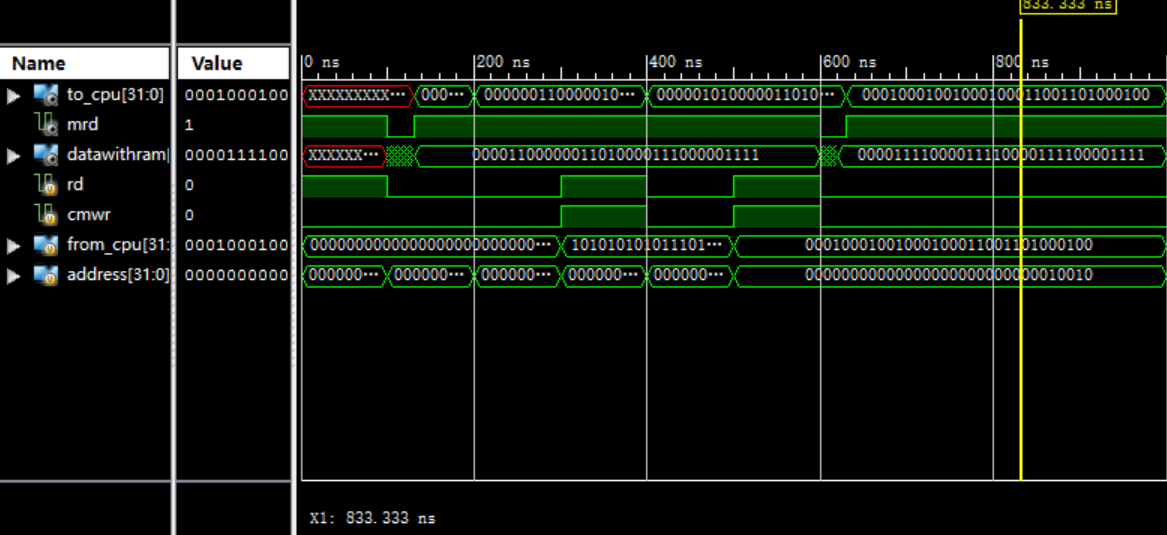
IV. EXPERIMENTAL RESULTS
