1. Introduction to DAC
Introduction to 1.1 DAC
DAC (Digital to analog converter) is a digital-to-analog converter that converts digital signals to analog signals. It functions opposite to ADC. In common digital signal systems, most sensor signals are converted to voltage signals, while ADC converts voltage analog signals to digital codes that are easy to store and process by computers. After processing by computers, ADC converts them to analog signals by ADC. DAC outputs a voltage analog signal, which is often used to drive certain executing devices, making it easy for humans to perceive. Such as the acquisition and restoration of audio signal is such a process.
The main technical indicators of DAC are as follows:
(1) Resolution
The resolution of a DAC is the change in the output analogue (voltage or current) corresponding to the change in the lowest significant bit (LSB) of the input number. It reflects the minimum change in the output analogue. The resolution is determined by the number of bits in the input number and can be expressed as FS/ (2^n). FS represents the full range input value, n is a binary number of bits. For a full range of 5V, the resolution is 5V/256=19.5mV for 8-bit DAC and 5V/4096=1.22mV for 12-bit DAC. Obviously, the higher the number of bits, the higher the resolution.
(2) Linearity
Linearity (also known as non-linear error) is the maximum deviation between the actual conversion characteristic curve and the ideal straight line characteristic. It is often expressed as a percentage of the full range. For example, +1% means that the difference between the actual output value and the theoretical value is within +1% of the full scale.
(3) Absolute and relative accuracy
Absolute precision refers to the maximum error between the actual output value and the theoretical value of the analogue value corresponding to any input number within the whole scale range. Absolute precision refers to the gain error of DAC (when the input number is all 1, the difference between the actual output value and the ideal output value), and the zero point error. Absolute precision (i.e. maximum error) should be less than 1 LSB. Relative and absolute precision mean the same thing, expressed as the percentage of maximum error relative to full scale.
(4) Establishment time
Establishment time refers to the time it takes for the output analog signal to reach +/1/2 LSB of the full scale value when the input digital quantity changes at full scale. It is a dynamic indicator of the D/A conversion rate. DAC can be divided into super-high speeds (< 1) depending on how long it takes to establish it μ S), High Speed (10-1) μ S), medium speed (100-10) μ S), low speed (> 100) μ S) several files.
How 1.1 DAC works
After understanding the basic concepts and characteristics of DAC, let's see how it works again. The following is a description of T-type resistance network DAC. Its internal structure is as follows:
Formula for calculating DAC output voltage: V0=Vref*z/256
Formula z denotes the amount of digits given by the single chip computer, vref is the reference voltage, we are usually connected to the system power supply, that is, 5V, value 256 denotes the DAC accuracy of 8 bits.
DAC consists mainly of digital registers, analog electronic switches, bit weight networks, The sum operational amplifier consists of a reference voltage source (or a constant current source). With each digit of the digital quantity stored in the digital register, the analog electronic switch of the corresponding bit is controlled separately, so that the bit of the number 1 produces a current value proportional to its bit weight in the bit weight network. The current values are summed by the operational amplifier and converted to the voltage value.
These analog electronic switches are followed by a voltage divider, such as a resistance. The number of analog switches depends on the accuracy of the DAC. Then N electronic switches divide the reference voltage into N parts (not equally divided oh), and these switches turn on or off according to the input binary data, bringing the voltage on the divider into the output circuit.
Introduction of 2 TLV5620 chip
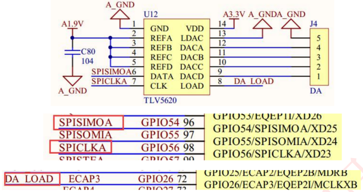
TLV5620 is a four-channel 8-bit analog-to-digital conversion (DAC) device, 3V-3.6V single power supply, 3-line serial bus, compatible with COMS devices, very easy to connect with microprocessor or microcontroller devices. It has 11-bit command words, including eight-bit data, two DAC selection bits, and one range bit, which allows selection of 1 or 2 times the output range. DAC registers are double buffered, allowing a complete set of new Values are written to the device, and all DAC outputs are updated simultaneously by controlling LDAC. DAC can produce an output voltage between the reference voltage and the GND one to two times.
This device is usually used in programmable voltage source, digital control amplifier/attenuator, mobile communication, automatic detection device, process monitoring and control, signal synthesis and other fields.
The function of TLV5620 chip pin is described as follows:
The formula for calculating the output voltage of each DAC channel is as follows:
REF is the reference voltage for the chip TLV5620. VREFA, B, C, D are connected to 1.9V on the development board, so REF=1.9V. CODE is a numeric value with a range of 0-255, RNG is one of the serial control words, and the range of values is 0 or 1.
When TLV5620 chip is used for DAC conversion, there are two ways to load data, one is through the LOAD pin control, when the LDAC foot is low level; The other is controlled by the LDAC pin. The first way we do this is to ground the LDAC foot and control the conversion and update through the LOAD foot. Let's look at the working sequence of the DAC chip, as shown in the following figure:
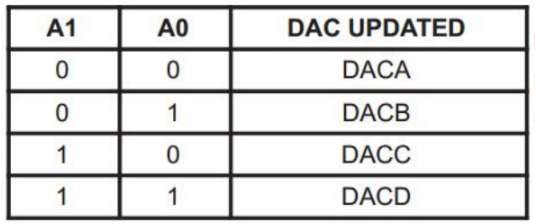
When DAC conversion is performed, data is locked to the data terminal along each descent of the CLK. When all data bits are fed in, LOAD transfers data from the serial input register to the selected DAC output channel for low pulses. The specific channel output is controlled by A1 and 20 bits, also known as channel selection bits, whose values correspond to the channel output as follows:
The RNG bit controls the output range of the DAC. When RNG =0, the output range is the applied reference voltage and GND; When RNG=1, the output range is twice the applied reference voltage and GND.
3. Hardware Design
4. Software Design
The function to be achieved in this chapter is: when the system is running, make four channels of TLV5620 output different voltage values every second, and display the numerical output through the serial port, the D1 indicator flashes to indicate that the system is running normally.
(1)DAC
void InitSpiaGpio()
{

   EALLOW;
/* Enable internal pull-up for the selected pins */
// Pull-ups can be enabled or disabled by the user.
// This will enable the pullups for the specified pins.
// Comment out other unwanted lines.

    GpioCtrlRegs.GPBPUD.bit.GPIO54 = 0;   // Enable pull-up on GPIO54 (SPISIMOA)
    GpioCtrlRegs.GPBPUD.bit.GPIO55 = 0;   // Enable pull-up on GPIO55 (SPISOMIA)
    GpioCtrlRegs.GPBPUD.bit.GPIO56 = 0;   // Enable pull-up on GPIO56 (SPICLKA)
    GpioCtrlRegs.GPBPUD.bit.GPIO57 = 0;   // Enable pull-up on GPIO57 (SPISTEA)


//    GpioCtrlRegs.GPBPUD.bit.GPIO54 = 0;   // Enable pull-up on GPIO54 (SPISIMOA)
//    GpioCtrlRegs.GPBPUD.bit.GPIO55 = 0;   // Enable pull-up on GPIO55 (SPISOMIA)
//    GpioCtrlRegs.GPBPUD.bit.GPIO56 = 0;   // Enable pull-up on GPIO56 (SPICLKA)
//    GpioCtrlRegs.GPBPUD.bit.GPIO57 = 0;   // Enable pull-up on GPIO57 (SPISTEA)

/* Set qualification for selected pins to asynch only */
// This will select asynch (no qualification) for the selected pins.
// Comment out other unwanted lines.

//    GpioCtrlRegs.GPAQSEL2.bit.GPIO16 = 3; // Asynch input GPIO16 (SPISIMOA)
//    GpioCtrlRegs.GPAQSEL2.bit.GPIO17 = 3; // Asynch input GPIO17 (SPISOMIA)
//    GpioCtrlRegs.GPAQSEL2.bit.GPIO18 = 3; // Asynch input GPIO18 (SPICLKA)
//    GpioCtrlRegs.GPAQSEL2.bit.GPIO19 = 3; // Asynch input GPIO19 (SPISTEA)

    GpioCtrlRegs.GPBQSEL2.bit.GPIO54 = 3; // Asynch input GPIO16 (SPISIMOA)
    GpioCtrlRegs.GPBQSEL2.bit.GPIO55 = 3; // Asynch input GPIO17 (SPISOMIA)
    GpioCtrlRegs.GPBQSEL2.bit.GPIO56 = 3; // Asynch input GPIO18 (SPICLKA)
    GpioCtrlRegs.GPBQSEL2.bit.GPIO57 = 3; // Asynch input GPIO19 (SPISTEA)


/* Configure SPI-A pins using GPIO regs*/
// This specifies which of the possible GPIO pins will be SPI functional pins.
// Comment out other unwanted lines.

//    GpioCtrlRegs.GPAMUX2.bit.GPIO16 = 1; // Configure GPIO16 as SPISIMOA
//    GpioCtrlRegs.GPAMUX2.bit.GPIO17 = 1; // Configure GPIO17 as SPISOMIA
//    GpioCtrlRegs.GPAMUX2.bit.GPIO18 = 1; // Configure GPIO18 as SPICLKA
//    GpioCtrlRegs.GPAMUX2.bit.GPIO19 = 1; // Configure GPIO19 as SPISTEA

    GpioCtrlRegs.GPBMUX2.bit.GPIO54 = 1; // Configure GPIO54 as SPISIMOA
    GpioCtrlRegs.GPBMUX2.bit.GPIO55 = 1; // Configure GPIO55 as SPISOMIA
    GpioCtrlRegs.GPBMUX2.bit.GPIO56 = 1; // Configure GPIO56 as SPICLKA
    GpioCtrlRegs.GPBMUX2.bit.GPIO57 = 1; // Configure GPIO57 as SPISTEA

    EDIS;
}

void TLV5620_Init(void)
{
	EALLOW;
	SysCtrlRegs.PCLKCR0.bit.SPIAENCLK = 1;   // SPI-A
	EDIS;

	/*Initialize GPIO;*/
	InitSpiaGpio();

	EALLOW;
	GpioCtrlRegs.GPAMUX2.bit.GPIO26 = 0; // Configure GPIO as a GPIO port
	GpioCtrlRegs.GPADIR.bit.GPIO26 = 1;      // Define GPIO Output Pin
	GpioCtrlRegs.GPAPUD.bit.GPIO26 = 0;      // Prohibit GPIO pins
	EDIS;

	SpiaRegs.SPICCR.all =0x0a;///Initial state, data rising along output, self-test prohibited, 11-bit data mode
	SpiaRegs.SPICTL.all =0x0006; // Enable host mode, normal phase, enable host to send, disable receive
		                            //Overflow interrupt, prohibit SPI interrupt;
	SpiaRegs.SPIBRR =0x0031;	//SPI baud rate = 37.5M/50 	= 0.75MHZ;
	SpiaRegs.SPICCR.all =0x8a; //Exit the initial state;
	SpiaRegs.SPIPRI.bit.FREE = 1;  // Free-running

	SET_LOAD;
}


///You need to know what each variable defined here means. channel is the address of four channels (00, 01, 10, 11)
/// rng is a multiple of the output range and can be either 0 or 1.
/// dat is 0~256 data
void DAC_SetChannelData(unsigned char channel,unsigned char rng,unsigned char dat)
{
	Uint16 dacvalue=0;

	//Note that the valid data here is 11 bits and is also defined in the SPI initialization
	dacvalue = ((channel<<14) | (rng<<13) | (dat<<5));

	while(SpiaRegs.SPISTS.bit.BUFFULL_FLAG ==1);//Determines whether the send buffer of the SPI is empty, equal to 0 writable data
	SpiaRegs.SPITXBUF = dacvalue;	//Write sent data to SPI send buffer
	while( SpiaRegs.SPISTS.bit.BUFFULL_FLAG==1);		//Start trivial data when the send buffer is full of flags

	ClEAR_LOAD;
	DELAY_US(2);

	SET_LOAD;
	DELAY_US(10);

}
void main()
{
	int i=0;
	Uint16 dacvalue=64;
	float dac_vol;
	Uint16 dac_temp=0;
	char dacbuf[6];


	InitSysCtrl();
	InitPieCtrl();
	IER = 0x0000;
	IFR = 0x0000;
	InitPieVectTable();

	LED_Init();
	TIM0_Init(150,200000);//200ms
	UARTa_Init(4800);
	TLV5620_Init();

	while(1)
	{
		i++;
		if(i%1000==0)
		{
			DAC_SetChannelData(0,0,dacvalue);
			dac_vol=dacvalue*1.9/255;
			dac_temp=dac_vol*100;
			dacbuf[0]=dac_temp/100+0x30;
			dacbuf[1]='.';
			dacbuf[2]=dac_temp%100/10+0x30;
			dacbuf[3]=dac_temp%100%10+0x30;
			dacbuf[4]='V';
			dacbuf[5]='\0';
			UARTa_SendString("\r\nCH1_VOL=");
			UARTa_SendString(dacbuf);

			DAC_SetChannelData(1,0,dacvalue*2);
			dac_vol=dacvalue*2*1.9/255;
			dac_temp=dac_vol*100;
			dacbuf[0]=dac_temp/100+0x30;
			dacbuf[1]='.';
			dacbuf[2]=dac_temp%100/10+0x30;
			dacbuf[3]=dac_temp%100%10+0x30;
			dacbuf[4]='V';
			dacbuf[5]='\0';
			UARTa_SendString("\r\nCH2_VOL=");
			UARTa_SendString(dacbuf);

			DAC_SetChannelData(2,0,dacvalue*3);
			dac_vol=dacvalue*3*1.9/255;
			dac_temp=dac_vol*100;
			dacbuf[0]=dac_temp/100+0x30;
			dacbuf[1]='.';
			dacbuf[2]=dac_temp%100/10+0x30;
			dacbuf[3]=dac_temp%100%10+0x30;
			dacbuf[4]='V';
			dacbuf[5]='\0';
			UARTa_SendString("\r\nCH3_VOL=");
			UARTa_SendString(dacbuf);

			DAC_SetChannelData(3,0,dacvalue*4-1);
			dac_vol=dacvalue*4*1.9/255;
			dac_temp=dac_vol*100;
			dacbuf[0]=dac_temp/100+0x30;
			dacbuf[1]='.';
			dacbuf[2]=dac_temp%100/10+0x30;
			dacbuf[3]=dac_temp%100%10+0x30;
			dacbuf[4]='V';
			dacbuf[5]='\0';
			UARTa_SendString("\r\nCH4_VOL=");
			UARTa_SendString(dacbuf);
		}
		DELAY_US(1*1000);
	}
}
(2)DAC_ADC
void InitSpiaGpio()
{

   EALLOW;
/* Enable internal pull-up for the selected pins */
// Pull-ups can be enabled or disabled by the user.
// This will enable the pullups for the specified pins.
// Comment out other unwanted lines.

    GpioCtrlRegs.GPBPUD.bit.GPIO54 = 0;   // Enable pull-up on GPIO54 (SPISIMOA)
    GpioCtrlRegs.GPBPUD.bit.GPIO55 = 0;   // Enable pull-up on GPIO55 (SPISOMIA)
    GpioCtrlRegs.GPBPUD.bit.GPIO56 = 0;   // Enable pull-up on GPIO56 (SPICLKA)
    GpioCtrlRegs.GPBPUD.bit.GPIO57 = 0;   // Enable pull-up on GPIO57 (SPISTEA)


//    GpioCtrlRegs.GPBPUD.bit.GPIO54 = 0;   // Enable pull-up on GPIO54 (SPISIMOA)
//    GpioCtrlRegs.GPBPUD.bit.GPIO55 = 0;   // Enable pull-up on GPIO55 (SPISOMIA)
//    GpioCtrlRegs.GPBPUD.bit.GPIO56 = 0;   // Enable pull-up on GPIO56 (SPICLKA)
//    GpioCtrlRegs.GPBPUD.bit.GPIO57 = 0;   // Enable pull-up on GPIO57 (SPISTEA)

/* Set qualification for selected pins to asynch only */
// This will select asynch (no qualification) for the selected pins.
// Comment out other unwanted lines.

//    GpioCtrlRegs.GPAQSEL2.bit.GPIO16 = 3; // Asynch input GPIO16 (SPISIMOA)
//    GpioCtrlRegs.GPAQSEL2.bit.GPIO17 = 3; // Asynch input GPIO17 (SPISOMIA)
//    GpioCtrlRegs.GPAQSEL2.bit.GPIO18 = 3; // Asynch input GPIO18 (SPICLKA)
//    GpioCtrlRegs.GPAQSEL2.bit.GPIO19 = 3; // Asynch input GPIO19 (SPISTEA)

    GpioCtrlRegs.GPBQSEL2.bit.GPIO54 = 3; // Asynch input GPIO16 (SPISIMOA)
    GpioCtrlRegs.GPBQSEL2.bit.GPIO55 = 3; // Asynch input GPIO17 (SPISOMIA)
    GpioCtrlRegs.GPBQSEL2.bit.GPIO56 = 3; // Asynch input GPIO18 (SPICLKA)
    GpioCtrlRegs.GPBQSEL2.bit.GPIO57 = 3; // Asynch input GPIO19 (SPISTEA)


/* Configure SPI-A pins using GPIO regs*/
// This specifies which of the possible GPIO pins will be SPI functional pins.
// Comment out other unwanted lines.

//    GpioCtrlRegs.GPAMUX2.bit.GPIO16 = 1; // Configure GPIO16 as SPISIMOA
//    GpioCtrlRegs.GPAMUX2.bit.GPIO17 = 1; // Configure GPIO17 as SPISOMIA
//    GpioCtrlRegs.GPAMUX2.bit.GPIO18 = 1; // Configure GPIO18 as SPICLKA
//    GpioCtrlRegs.GPAMUX2.bit.GPIO19 = 1; // Configure GPIO19 as SPISTEA

    GpioCtrlRegs.GPBMUX2.bit.GPIO54 = 1; // Configure GPIO54 as SPISIMOA
    GpioCtrlRegs.GPBMUX2.bit.GPIO55 = 1; // Configure GPIO55 as SPISOMIA
    GpioCtrlRegs.GPBMUX2.bit.GPIO56 = 1; // Configure GPIO56 as SPICLKA
    GpioCtrlRegs.GPBMUX2.bit.GPIO57 = 1; // Configure GPIO57 as SPISTEA

    EDIS;
}

void TLV5620_Init(void)
{
	EALLOW;
	SysCtrlRegs.PCLKCR0.bit.SPIAENCLK = 1;   // SPI-A
	EDIS;

	/*Initialize GPIO;*/
	InitSpiaGpio();

	EALLOW;
	GpioCtrlRegs.GPAMUX2.bit.GPIO26 = 0; // Configure GPIO as a GPIO port
	GpioCtrlRegs.GPADIR.bit.GPIO26 = 1;      // Define GPIO Output Pin
	GpioCtrlRegs.GPAPUD.bit.GPIO26 = 0;      // Prohibit GPIO pins
	EDIS;

	SpiaRegs.SPICCR.all =0x0a;///Initial state, data rising along output, self-test prohibited, 11-bit data mode
	SpiaRegs.SPICTL.all =0x0006; // Enable host mode, normal phase, enable host to send, disable receive
		                            //Overflow interrupt, prohibit SPI interrupt;
	SpiaRegs.SPIBRR =0x0031;	//SPI baud rate = 37.5M/50 	= 0.75MHZ;
	SpiaRegs.SPICCR.all =0x8a; //Exit the initial state;
	SpiaRegs.SPIPRI.bit.FREE = 1;  // Free-running

	SET_LOAD;
}


///You know what each variable defined here means, add is the address of four channels (00, 01, 10, 11)
/// RNG is a multiple of the output range and can be 0 or 1.
/// VOL is 0~256 data
void DAC_SetChannelData(unsigned char channel,unsigned char rng,unsigned char dat)
{
	Uint16 dacvalue=0;

	//Note that the valid data here is 11 bits and is also defined in the SPI initialization
	dacvalue = ((channel<<14) | (rng<<13) | (dat<<5));

	while(SpiaRegs.SPISTS.bit.BUFFULL_FLAG ==1);//Determines whether the send buffer of the SPI is empty, equal to 0 writable data
	SpiaRegs.SPITXBUF = dacvalue;	//Write sent data as SPI send buffer
	while( SpiaRegs.SPISTS.bit.BUFFULL_FLAG==1);		//Start trivial data when the send buffer is full of flags

	ClEAR_LOAD;
	DELAY_US(2);

	SET_LOAD;
	DELAY_US(10);

}
#define ADC_MODCLK 3
#define ADC_CKPS   0x1   // ADC module clock = HSPCLK/2*ADC_CKPS   = 25.0MHz/(1*2) = 12.5MHz
#define ADC_SHCLK  0xf   // S/H width in ADC module periods                        = 16 ADC clocks


void ADC_Init(void)
{
	EALLOW;
	SysCtrlRegs.PCLKCR0.bit.ADCENCLK = 1;    // ADC
	EDIS;

	// Specific clock setting for this example:
	EALLOW;
	SysCtrlRegs.HISPCP.all = ADC_MODCLK;	// HSPCLK = SYSCLKOUT/ADC_MODCLK
	EDIS;

	InitAdc();  // For this example, init the ADC

	// Specific ADC setup for this example:
	AdcRegs.ADCTRL1.bit.ACQ_PS = ADC_SHCLK;
	AdcRegs.ADCTRL3.bit.ADCCLKPS = ADC_CKPS;
	AdcRegs.ADCTRL1.bit.SEQ_CASC = 1;        // 1  Cascaded mode
	AdcRegs.ADCCHSELSEQ1.bit.CONV00 = 0x0;
	AdcRegs.ADCTRL1.bit.CONT_RUN = 1;       // Setup continuous run

	// Start SEQ1
	AdcRegs.ADCTRL2.all = 0x2000;

}

Uint16 Read_ADCValue(void)
{
	while (AdcRegs.ADCST.bit.INT_SEQ1== 0);
	AdcRegs.ADCST.bit.INT_SEQ1_CLR = 1;
	return AdcRegs.ADCRESULT0>>4;
}
void main()
{
	int i=0;
	Uint16 dacvalue=64;
	float dac_vol;
	Uint16 dac_temp=0;
	char dacbuf[6];

	float adc_vol;
	Uint16 adc_temp=0;


	InitSysCtrl();
	InitPieCtrl();
	IER = 0x0000;
	IFR = 0x0000;
	InitPieVectTable();

	LED_Init();
	TIM0_Init(150,200000);//200ms
	UARTa_Init(4800);
	TLV5620_Init();
	ADC_Init();

	while(1)
	{
		i++;
		if(i%1000==0)
		{

			DAC_SetChannelData(1,0,dacvalue*2);
			dac_vol=dacvalue*2*1.9/255;
			dac_temp=dac_vol*100;
			dacbuf[0]=dac_temp/100+0x30;
			dacbuf[1]='.';
			dacbuf[2]=dac_temp%100/10+0x30;
			dacbuf[3]=dac_temp%100%10+0x30;
			dacbuf[4]='V';
			dacbuf[5]='\0';
			UARTa_SendString("\r\nCH2_VOL=");
			UARTa_SendString(dacbuf);

			adc_vol=(float)Read_ADCValue()*3.3/4095;
			adc_temp=adc_vol*100;
			dacbuf[0]=adc_temp/100+0x30;
			dacbuf[1]='.';
			dacbuf[2]=adc_temp%100/10+0x30;
			dacbuf[3]=adc_temp%100%10+0x30;
			dacbuf[4]='V';
			dacbuf[5]='\0';
			UARTa_SendString("\r\nADC_CH1_VOL=");
			UARTa_SendString(dacbuf);
		}
		DELAY_US(1*1000);
	}
}