DS1302 real time clock module
Chip Manual: datasheet pdf index DS1302 Datasheet
The clock chip DS1302 contains a real-time clock / calendar and 31 byte static RAM. The communication with MCU is carried out by 3-wire synchronous serial mode.
1. DS1302 pin
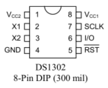
| PIN | Pin description |
|---|---|
| X1,X2 | The crystal oscillator is connected to the pin, and the crystal oscillator frequency is 32.768kHz |
| RST | Reset pin, high level start input and output, low level end input and output |
| I/O | Data input / output pin |
| SCLK | Serial clock input pin |
| GND | Ground pin |
| Vcc1,Vcc2 | Working power supply, backup working power supply |
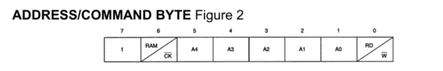
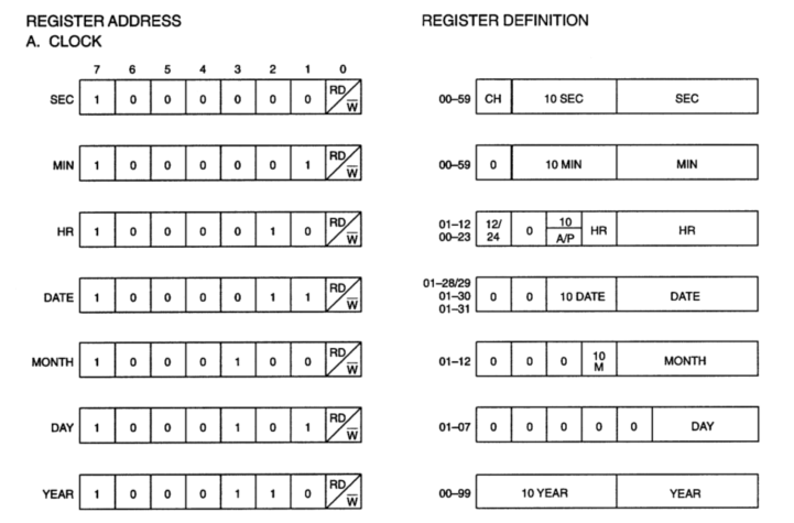
2. Command byte
The command byte is shown in the following figure:
Each data transmission is initiated by a command byte, and MSB (Bit7) must be logic 1. If it is 0, writing to DS1302 will be disabled.
If the logic of bit 6 is 0, specify clock / calendar data; If the logic is 1, the RAM data is specified.
Bits 1 to 5 specify the register to be input or output, and LSB (bit 0) specifies the write operation at logic 0 or the read operation (output) at logic 0.
The command byte is always input from LSB (bit 0)
3. Reset and clock control
All data transmission is initiated by driving the RST high input.
RST input has two functions:
- First, RST turns on the control logic to allow access to the shift register of the address / command sequence.
- Second, the RST signal provides a method for terminating single byte or multi byte data transmission.
A clock cycle is a sequence of falling and rising edges. For data input, the data must be valid at the rising edge of the clock, and the data bits are output at the lower edge of the time type. (that is, write data is on the rising edge of the clock and read data is on the falling edge of the clock)
If the RST input is low, all data transmission is terminated and the IO pin enters the high resistance state,
When powered on, RST must be logic 0 and know that VCC > 2.0V. Meanwhile, when RST is driven to logic 1, SCLK must be at logic 0. (look at the input and output diagram below. At first, RST is low, SCLK is low, then RST is high, and then data transmission starts.)
4. Data input and output
(1) Data input
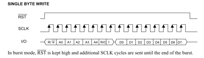
After inputting a write command byte in eight SCLK cycles (see the I/O line in the figure above, the first is to input the write command byte in eight SCLK cycles),
Input a data byte on the rising edge of the next 8 SCLK cycles (note that in the figure above, each byte input is from the rising edge),
If the data is entered from bit 0, the additional SCLK cycle is ignored.
Example:
- Each time CLK is pulled down, IO gives a value, and CLK is pulled up
- Dat always gives the IO value from the lowest bit, so dat should be shifted by 1 bit to the right
void DS1302_WByte(uchar dat)
{
	uchar i;
	for(i = 8; i > 0; i--)			// It can also be seen from the figure that the data is input from D0
	{
		DS1302_CLK = 0;				// Clock line to low level
		Delay4Us();					// delayed
		DS1302_IO = dat & 0x01;		// IO input one byte
		DS1302_CLK = 1;				// Clock line pull up
		dat = dat >> 1;				// Shift data one bit to the right
	}
}
(2) Data output
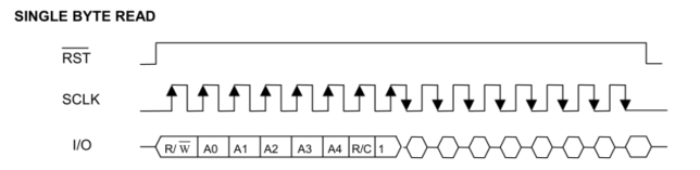
After 8 SCLK cycles of a read command byte are input, a data byte is output at the falling edge of the next 8 SCLK cycles.
Note that the first data bit to be transmitted occurs on the first falling edge after the last bit of the write command byte.
Additional SCLK cycles retransmit data bytes, which will occur inadvertently as long as RST remains high. Allows continuous highlighting of the read capability of the mode. In addition, the IO pins are three columns on each rising edge of SCLK. Data is output from bit 0.
uchar DS1302_RByte(void)
{
	uchar i,temp = 0;
	DS1302_IO = 1;
	for(i=8; i>0; i--)
	{
		DS1302_CLK=0;				// CLK clock is pulled down and ready to fetch data
		Delay4Us();
		temp = temp >> 1;			// First, the low position is in the high position, so you need to move right every time
		if( DS1302_IO == 1)			// When the IO pin is high, the data bit or operation is 0x80
		{
			temp = temp | 0x80;
		}
		DS1302_CLK=1;
		Delay4Us();
	}
	return temp;
}
5. Other sample functions
1) Write data to an address of ds1302
void DS1302_W_Addr_Dat(uchar addr, uchar dat)
{
	DS1302_RST = 0;
	DS1302_CLK = 0;
	DS1302_RST = 1;		// The reason for the first three lines is shown in the bold part of the last sentence over 3. Reset and clock control
	DS1302_WByte(addr);			// Address, command
	DS1302_WByte(dat);			// Write 1 byte of data, one byte is equal to 8 bits
	DS1302_CLK = 1;
	DS1302_RST = 0;
}
2) Read the data of an address in ds1302
void DS1302_R_All(uchar addr)
{
	uchar dat;
	DS1302_RST = 0;
	DS1302_CLK = 0;
	DS1302_RSt = 1;
	DS1302_WByte(addr | 0x01);			// Address, command
	dat = DS1302_RByte();				// Read 1 byte data
	DS1302_CLK=1;
	DS1302_RST=0;
	return(dat);
}
3) Read time and date
Register address
Sample program
// Define structure
typedef struct
{
	uchar Second;
	uchar Minute;
	uchar Hour;
	uchar Week;
	uchar Day;
	uchar Month;
	uchar Year;
	uchar DataString[9];
	uchar TimeString[9];
}TIMETYPE;

// Here is the address of the register
#define DS1302_SECOND      0x80
#define DS1302_MINUTE      0x82
#define DS1302_HOUR        0x84
#define DS1302_WEEK		   0x8A
#define DS1302_DAY		   0x86
#define DS1302_MONTH       0x88
#define DS1302_YEAR		   0x8C

// 0x70=0111 0000, 0x0F=0000 1111
// As can be seen from the above register address diagram, the upper four bits are the number stored on ten bits, and the fourth bit is the number stored on one bit
void DS1302_R_All( TIMETYPE *TIME)
{
	uchar Rtemp;
	Rtemp = DS1302_R_Addr(DS1302_SECOND);				// second
	Time->Second = ((Rtemp&0x70)>>4)*10 + (Rtemp & 0x0F);
	Rtemp = DS1302_R_Addr(DS1302_MINUTE);				// minute
	Time->Minute = ((Rtemp&0x70)>>4)*10 + (Rtemp & 0x0F);
	Rtemp = DS1302_R_Addr(DS1302_HOUR);					// hour
	Time->Hour = ((Rtemp&0x70)>>4)*10 + (Rtemp & 0x0F);
	Rtemp = DS1302_R_Addr(DS1302_DAY);					// day
	Time->Day = ((Rtemp&0x70)>>4)*10 + (Rtemp & 0x0F);
	Rtemp = DS1302_R_Addr(DS1302_WEEK);					// week
	Time->Week = ((Rtemp&0x70)>>4)*10 + (Rtemp & 0x0F);
	Rtemp = DS1302_R_Addr(DS1302_MONTH);				// month
	Time->Month = ((Rtemp&0x70)>>4)*10 + (Rtemp & 0x0F);
    Rtemp = DS1302_R_Addr(DS1302_YEAR);					// year
	Time->Year = ((Rtemp&0x70)>>4)*10 + (Rtemp & 0x0F);
}
4) ds1302 initialization
void DS1302_Init(void)

{
	uchar Second;
	DS1302_RST = 0;
	DS1302_CLK = 0;
	Second = DS1302_R_Addr(DS1302_SECOND);
	DS1302_W_Addr_Dat(0x8e, 0x00);
	DS1302_W_Addr_Dat(0x80, Second & 0x7f);
	DS1302_W_Addr_Dat(0x90, 0xa6);				// DS1302 register is configured with a diode and 4k Ω charging resistance
	DS1302_W_Addr_Dat(0x8E, 0x80);
}