1.ADC
- Sample and hold?
F28335 chip contains ADC peripherals to realize the conversion from analog quantity to digital quantity.
ADC conversion includes sample and hold quantization and coding; Sampling is to convert the continuous quantity in time into the discrete quantity in time, and save the sampling results until the next sampling is called hold - sample and hold circuit.
- DSP comes with ADC peripherals
The ADC of F28335 is 12 bits and has 16 channels (2 groups), but there is only one converter and two sample holders (S/H). The 16 bit result register returns the result of ADC conversion. The converted digital quantity:

The two terminals of the input signal of ADC acquisition module are: positive: ADCINAx and negative: ADCL0
- What is a sorter?
Because there is only one converter with 16 inputs, the sequencer is needed to control the order of conversion. - What is cascading / double sorting?
Change to a 16 state sequencer; 2 independent 8-state sorters - What is sequence / synchronization (SMODE_SEL)?
Sequence (0) is equivalent to serial, one at a time; Synchronization (1) is equivalent to parallel. One time corresponds to two groups A and B.
In fact, if there are no special requirements, direct cascade sorter + sequence / synchronization is enough.
2.SCI (two wires, one sending and one receiving)
- Serial communication refers to a communication mode in which data is transmitted bit by bit between peripherals and computers through data signal lines, ground wires, etc. it belongs to serial communication mode. SCI/SPI/IIC
- Serial port is an interface standard, which specifies the electrical standard of the interface, but does not specify the interface plug-in cable and the protocol used. RS232/485
- DSP28335 has three SCI serial ports. Since dsp has ttl level (1-2.4V; 0-0.4V), MAX232 needs to be used for level conversion.
- Main registers SCITXBUF, SCIRXBUF, baud rate generation
- SCI signal acceptance
The flag bit RXENA is 1, enabling the receiver to accept data.
The data reaches the SCIRXD pin and detects the start bit.
The data from the register to the accept buffer SCIRXBUF generates an interrupt request, and the flag bit RXRDY is 1, indicating that a new character has been accepted.
The program reads SCIRXBUF and the flag bit RXRDY is cleared - SCI signal transmission
TXENA is 1, enabling the transmitter. Write data to SCITXBUF register, TXRDY is low
The value in SCITXBUF enters the shift register and TXRDY becomes high. - Baud rate
3.ADC configuration
-
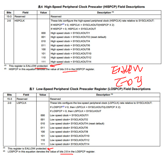
Peripheral high speed clock
ADC clock: CPS: 0, no frequency division for HSOCLK
-
Operation mode: CONT_RUN: 1 continuous operation
-
Cascade + sequence
Sorter mode: SEQ_CASC: 1 cascade
SMODE_SEL=0 default sequential sampling -
Max channels for initialization conversion_ Conv (max. 16)
Configure the conversion order CHSELxx, which determines the position of the final conversion result in the register.
For sequential sampling, the input pin is determined by the 4-bit value of the control register CONVxx, the highest bit determines the sample and hold buffer, and the other three bits define the specific input pin.
ADCCHSELSEQ1-4 contains CONV00-15; For example, if you want to input ADCINA0, assign - 0000 to CONVxx in the corresponding order (the first 0 represents group A and 000 represents pin 0)
About the result register: because it is a 12 bit ADC, only 12 bits are used, while the register is 16 bits. Therefore, the high 12 bits of ADCRESULTn are valid, so it needs to be shifted by 4.
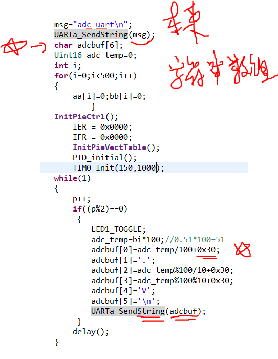
void ADC_Init(void)
{
EALLOW;
SysCtrlRegs.PCLKCR0.bit.ADCENCLK=1;//Turn on ADC clock
EDIS;
EALLOW;
SysCtrlRegs.HISPCP.all=3;//HISPCP frequency division 150M/2*3=25MHz
EDIS;
//Initialize adc
InitAdc();//TI's reference source calibration of ADC module is completed
//What we need to do, working mode, sampling mode, working frequency, sampling channel
AdcRegs.ADCTRL1.bit.ACQ_PS=0x0f;//Sampling filtering, smode is not set_ SEL default sequential sampling
AdcRegs.ADCTRL1.bit.SEQ_CASC=1;//cascade
AdcRegs.ADCTRL1.bit.CONT_RUN=1;//Continuous operation
AdcRegs.ADCTRL3.bit.ADCCLKPS=1;//No more frequency division
AdcRegs.ADCCHSELSEQ1.bit.CONV00=0x0;//ADCINA0
AdcRegs.ADCMAXCONV.bit.MAX_CONV1=0x0;//Maximum number of channels, 0-15
AdcRegs.ADCTRL2.all=0x2000;//Trigger source - software trigger
}
Uint16 Read_ADCValue(void)
{
	while(AdcRegs.ADCST.bit.INT_SEQ1==0);
	AdcRegs.ADCST.bit.INT_SEQ1_CLR=1;
	return AdcRegs.ADCRESULT0>>4;//The result of the conversion is shifted to the right. It was originally placed in the high 12 bits. Note the result0 here
}
Read this value in the main function:
float adc_vol;
adc_vol=(float)Read_ADCValue()*3.0/4095;
4.SCI configuration + float to str
#include "uart.h"
void UARTa_Init(Uint32 baud)
{
unsigned char scihbaud=0;
unsigned char scilbaud=0;
Uint16 scibaud=0;
scibaud=37500000/(8*baud)-1;
scihbaud=scibaud>>8;
scilbaud=scibaud&0xff;
EALLOW;
SysCtrlRegs.PCLKCR0.bit.SCIAENCLK = 1; // SCI-A
EDIS;
InitSciaGpio();
//Initalize the SCI FIFO
SciaRegs.SCIFFTX.all=0xE040;
SciaRegs.SCIFFRX.all=0x204f;
SciaRegs.SCIFFCT.all=0x0;
// Note: Clocks were turned on to the SCIA peripheral
// in the InitSysCtrl() function
SciaRegs.SCICCR.all =0x0007; // 1 stop bit, No loopback
// No parity,8 char bits,
// async mode, idle-line protocol
SciaRegs.SCICTL1.all =0x0003; // enable TX, RX, internal SCICLK,
// Disable RX ERR, SLEEP, TXWAKE
SciaRegs.SCICTL2.all =0x0003;
SciaRegs.SCICTL2.bit.TXINTENA =1;
SciaRegs.SCICTL2.bit.RXBKINTENA =1;
SciaRegs.SCIHBAUD =scihbaud; // 9600 baud @LSPCLK = 37.5MHz.
SciaRegs.SCILBAUD =scilbaud;
// SciaRegs.SCICCR.bit.LOOPBKENA =1; // Enable loop back
SciaRegs.SCICTL1.all =0x0023; // Relinquish SCI from Reset
}
// Transmit a character from the SCI'
void UARTa_SendByte(int a)
{
while (SciaRegs.SCIFFTX.bit.TXFFST != 0);
SciaRegs.SCITXBUF=a;
}
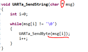
void UARTa_SendString(char * msg)
{
int i=0;
while(msg[i] != '\0')
{
UARTa_SendByte(msg[i]);
i++;
}
}
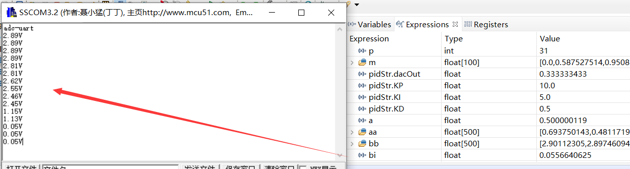
5. Effect
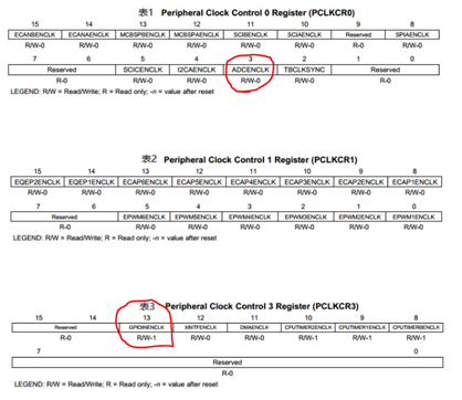
6. About peripheral clock configuration PCLKCRx
Dsp28335 generates the frequency doubling clock signal CLKIN through the external clock signal, OSC and PLL. After CLKIN passes through the CPU, it generates the clock SYSCLKOUT (the frequencies of CLKIN and SYSCLKOUT are the same). SYSCLKOUT provides clock signals to all internal and external devices.
In order to achieve low power consumption and provide high and low frequency clock signals, SYSCLKOUT needs to be further divided.
Except that SPI, SCI and McBSP modules use low-frequency clock and ADC uses high-frequency clock, other peripheral modules use SYSCLKOUT clock.
How to save electricity?
- Peripheral clock control register PCLKCR -- the unused peripheral will not turn on its clock 0
- High and low frequency peripheral clock division registers HISPCP, LOSPCP -- set rate
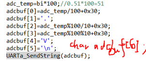
Char and char * and char []
- Char *str1="abcd";
String constants, stored in static storage, are read-only. Is to assign the first address of the anonymous array to the object. It is equivalent to that str1 stores the address of the anonymous array "abcd". At this time, char *str2=str1 means that the address of str1 is given to str2.
- Char str2[ ]="abcd";
String array is used to copy the contents of anonymous functions to the space of the object. Can str2[1] = 'a'; str2 + + is not allowed; - Char * str3 = & STR2 is str3 [] = "abcd";
But char [] can be implicitly converted to char *; That is, the function input (char * msg) has an array of str2 []; Is to use this function.
Or directly
char msg="123";
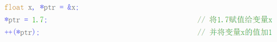
*And&
*Indicates a pointer& Indicates the address
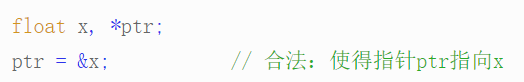
But if ptr is a pointer, * ptr is equivalent to the variable x