preface
FIFO(First in First out) represents the first out of the first in data and the last out of the data. It is a very important module in FPGA applications. It is widely used in data caching, cross clock domain data processing and so on. Vivado software provides the IP core of FIFO. We only need to instantiate a FIFO through the IP core, and write and read the data stored in FIFO according to the read-write timing of FIFO.
1, Introduction to FIFO
FIFO adds many functions on the basis of RAM. The typical structure of FIFO is shown in the figure below.
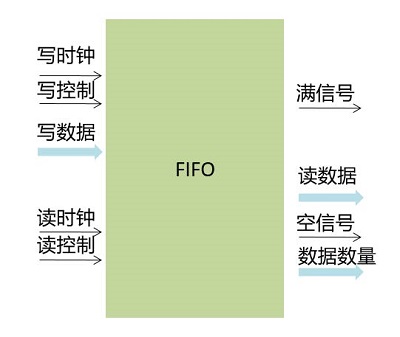
FIFO is mainly divided into two parts: read and write. The status signal includes empty signal and full signal, as well as data quantity status signal. The biggest difference between FIFO and RAM is that there is no address line, so random address reading data cannot be carried out (random reading data is the data that can read a certain address arbitrarily). This advantage is that there is no need to control the address line frequently.
Although the user cannot see the address line, there is still an address operation inside the FIFO, which is used to control the read-write interface of RAM. Its address is shown in the following figure during read-write operation.
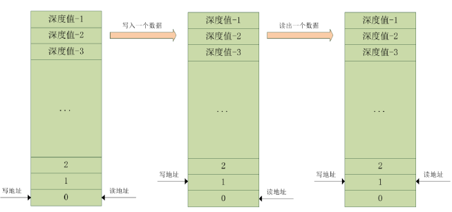
The depth value in the figure above is the maximum number of data that can be stored in a FIFO.
In the initial state, the read and write addresses are all 0. After writing a data into the FIFO, the write address is increased by 1. After reading a data from the FIFO, the read address is increased by 1. At this time, the FIFO state is empty, because a data is written and another data is read out.
If the frequency of writing data is faster than that of reading data, the FIFO will be full, that is, when it reaches the depth value. If the FIFO is full and continues to write data, it will overflow.
If the frequency of reading data is faster than that of writing data, the FIFO will be empty. Therefore, it is an arduous task to judge whether the FIFO is empty or full, grasp the frequency of reading data and writing data, and keep the data in the FIFO all the time.
According to the similarities and differences of read-write clocks, FIFO can be divided into synchronous FIFO (the same clock for read and write) and asynchronous FIFO (different clocks for read and write). Synchronous FIFO control is relatively simple. This experiment mainly introduces the control of asynchronous FIFO, in which the read clock is 75MHz and the write clock is 100MHz.
The port definitions in this experiment are as follows.
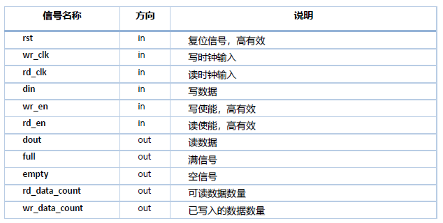
FIFO data writing and reading are operated according to the rising edge of the clock when wr_ Write FIFO data when en signal is high, when almost_ When the full signal is valid, it means that the FIFO can only write one more data. Once a data is written, the full signal will be pulled up. If in the case of full, wr_en is still valid, that is, if you continue to write data to FIFO, the overflow of FIFO will be valid, indicating overflow.
When Rd_ Read FIFO data when en signal is high. The data is valid in the next cycle. Valid is the data valid signal, almost_empty indicates that there is another data read. When another data is read, the empty signal is valid. If you continue to read, underflow is valid, indicating underflow. At this time, the read data is invalid.
2, Add FIFO IP core
First create a file called fifo_test project. See the following for the detailed steps of creating the project: Use of Vivado software -- Taking the alternating flashing of led as an example.
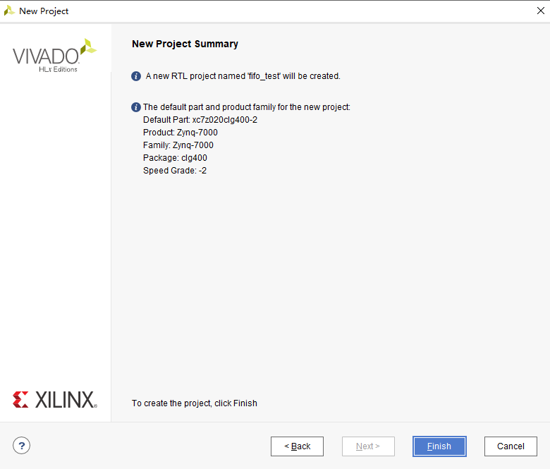
After the new project arrives at the interface shown in the figure below, click Finish to complete the creation of the project.
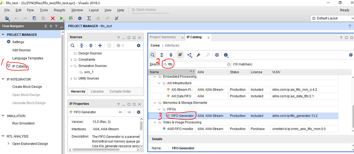
After the project is created, find the FIFO Generator according to the sequence number in the figure below and double-click to open it.
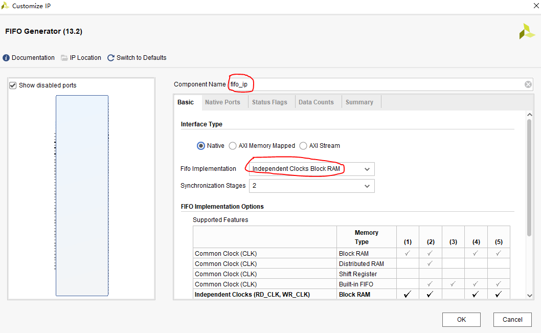
In the pop-up configuration page, first change the Component Name to "fifo_ip". Here you can choose whether the read-write clocks are separated or the same. Generally speaking, we use FIFO. In order to cache data, the clock speeds on both sides are usually different, so the independent clock is the most commonly used. Here we choose "Independent Clocks Block RAM".
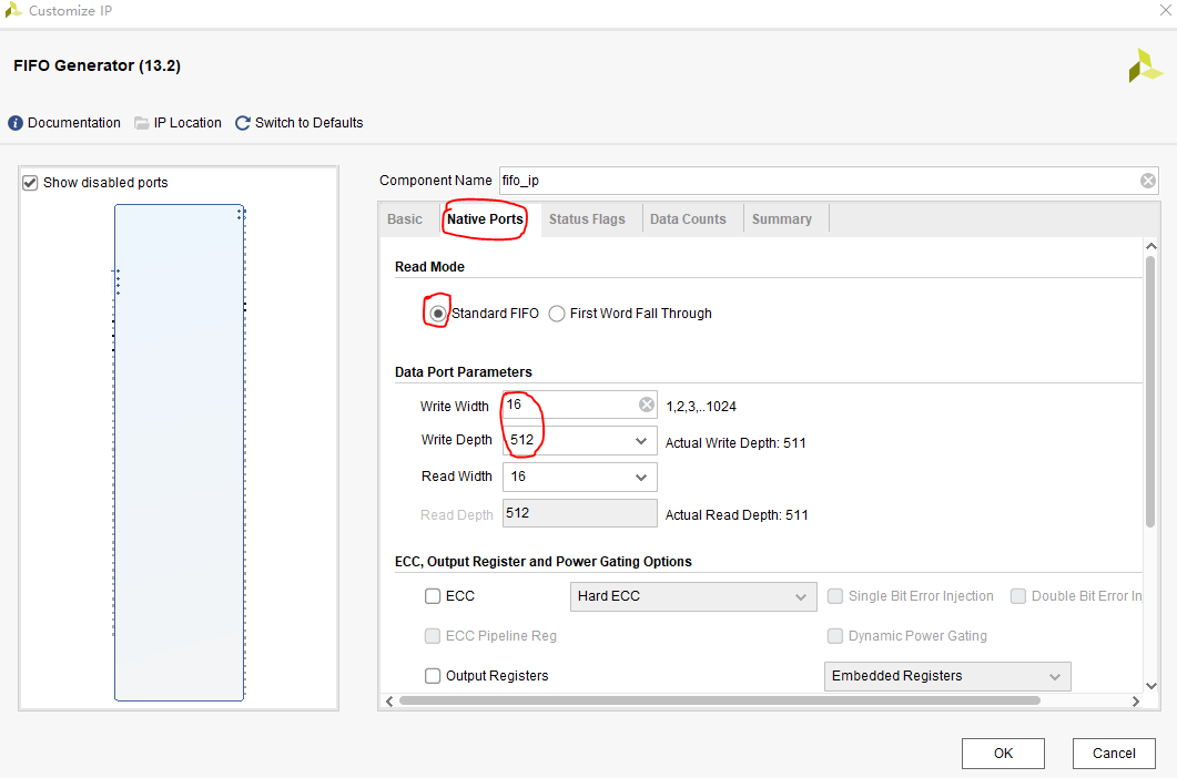
In the Native Ports configuration interface, select the data bit width of 16 and the FIFO depth of 512.
There are two modes of Read Mode. One is Standard FIFO, that is, Standard FIFO. The data lags behind the read signal by one cycle; Another method is First Word Fall Through, that is, data prefetching mode, referred to as FWFT mode, that is, FIFO will take out a data in advance. When the read signal is valid, the corresponding data is also valid. Here, select Standard FIFO.
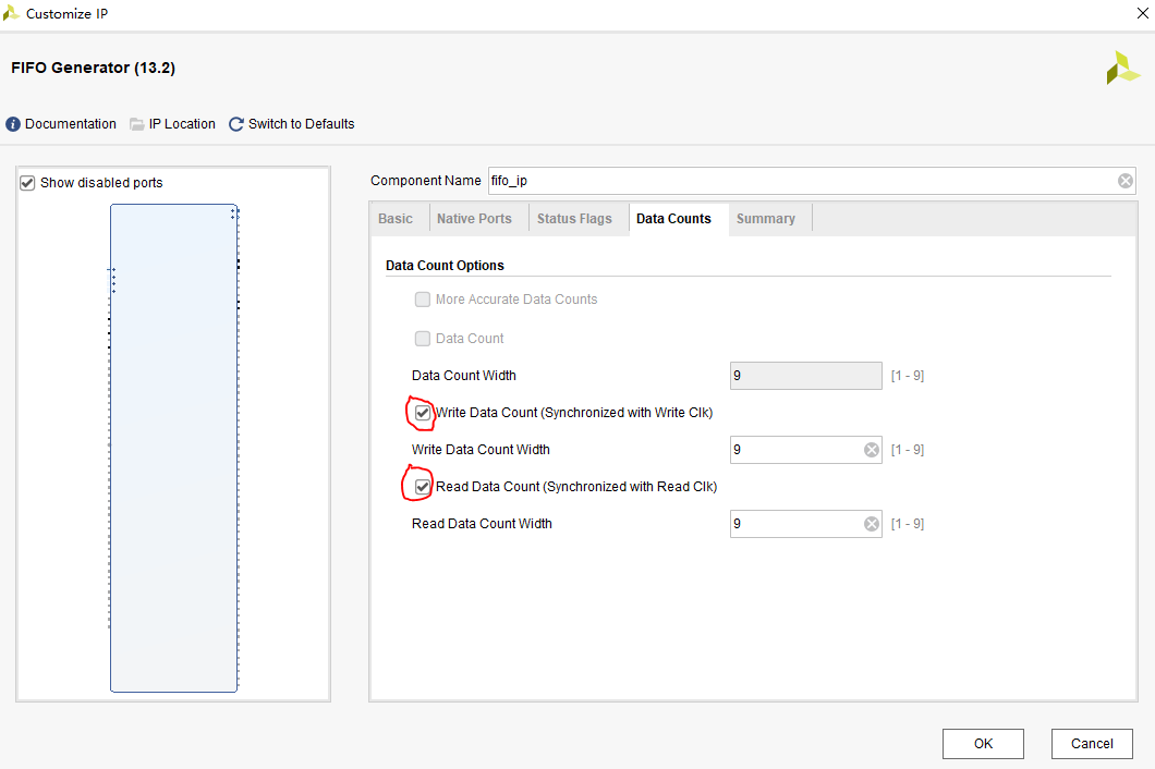
Switch to the Data Counts configuration interface and check the Write Data Count and Read Data Count options, so that we can see how much data is in the FIFO through these two values.
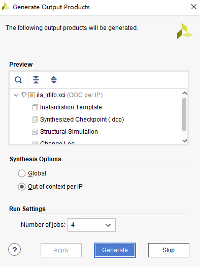
Here, the part to be modified has been completed, and the parameters under other options can remain the default. Click OK to pop up the following dialog box.
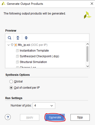
Click Generate to Generate FIFO IP.
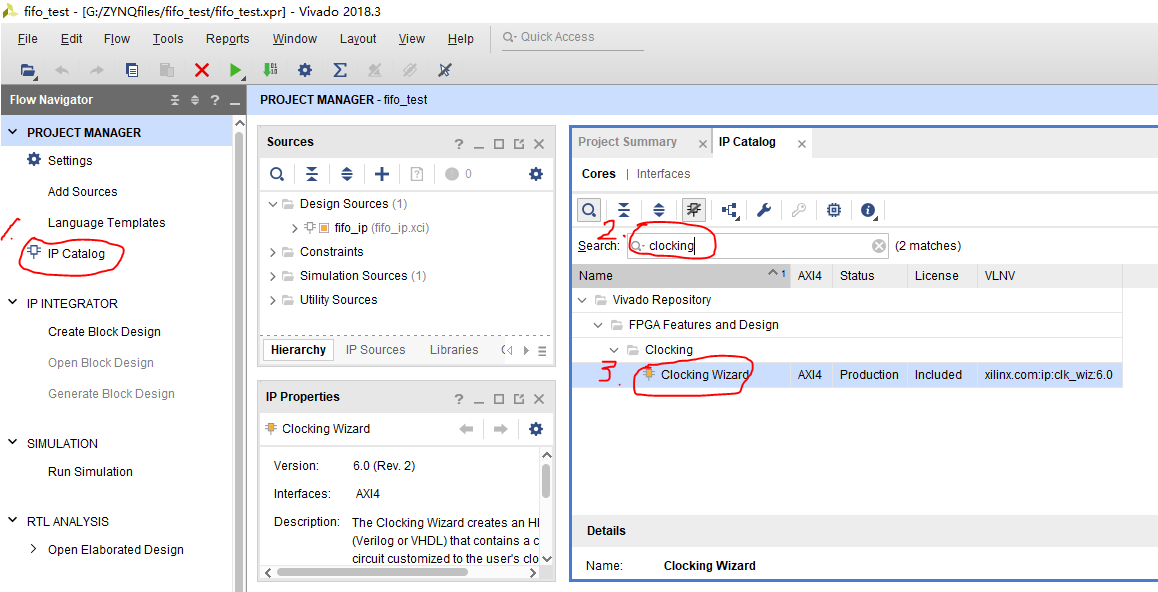
3, Add PLL IP core
PLL is used to generate two channels of 100MHz and 75MHz clocks, which are used for writing clock and reading clock respectively. The frequency of writing clock is higher than that of reading clock.
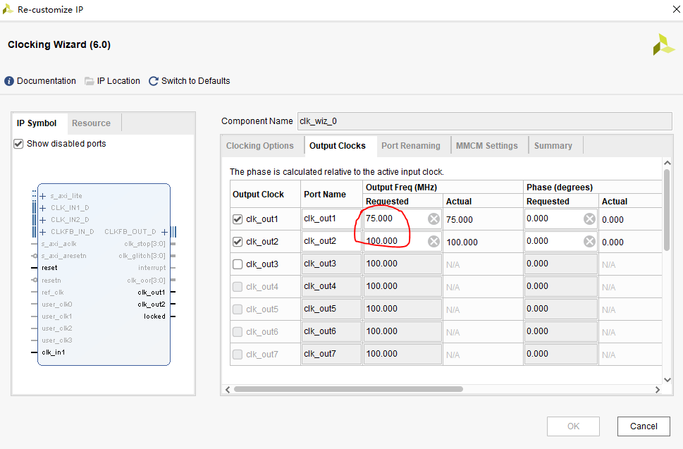
Follow the sequence number in the figure below to find the Clocking Wizard and double-click to open it.
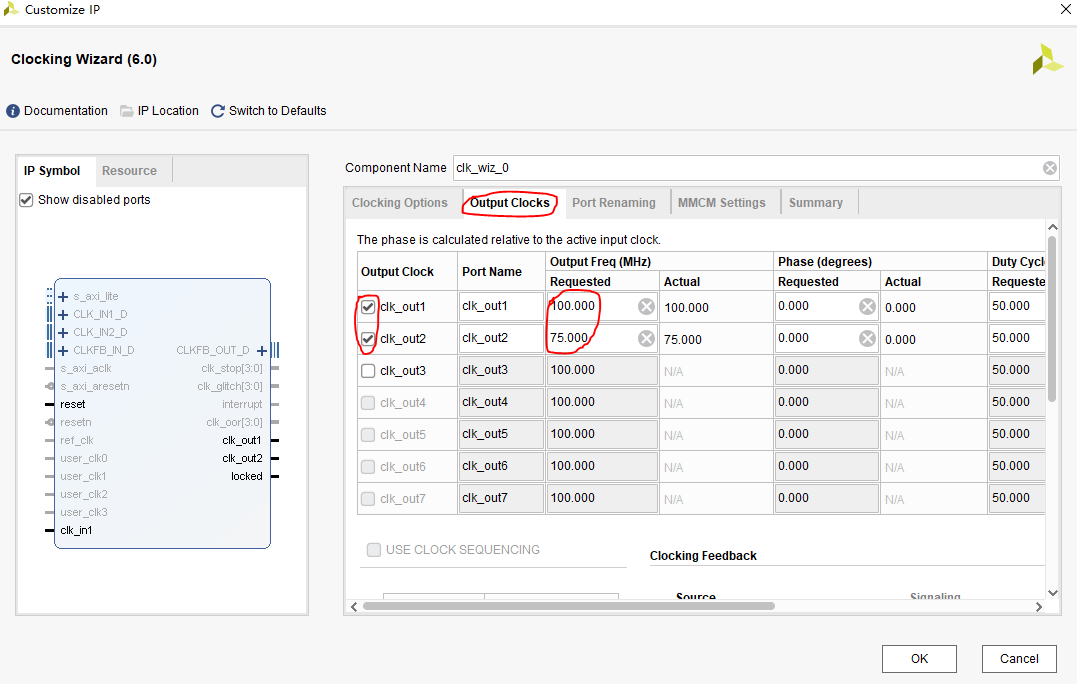
Add two clock outputs under Output Clocks, with frequencies of 100MHz and 75MHz. The others remain the default. Click OK.
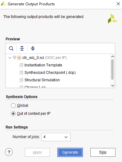
Click Generate IP core to Generate the clock.
4, Add ILA IP core
This experiment needs to instantiate two logic analyzers to connect the signals of write channel and read channel respectively.
First, add the ILA IP core of the write channel, as shown in the figure below.
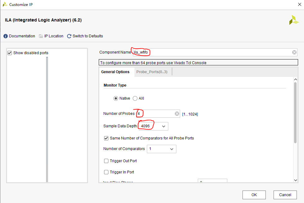
Set the number of bits for each write channel probe according to the code, as shown in the figure below.
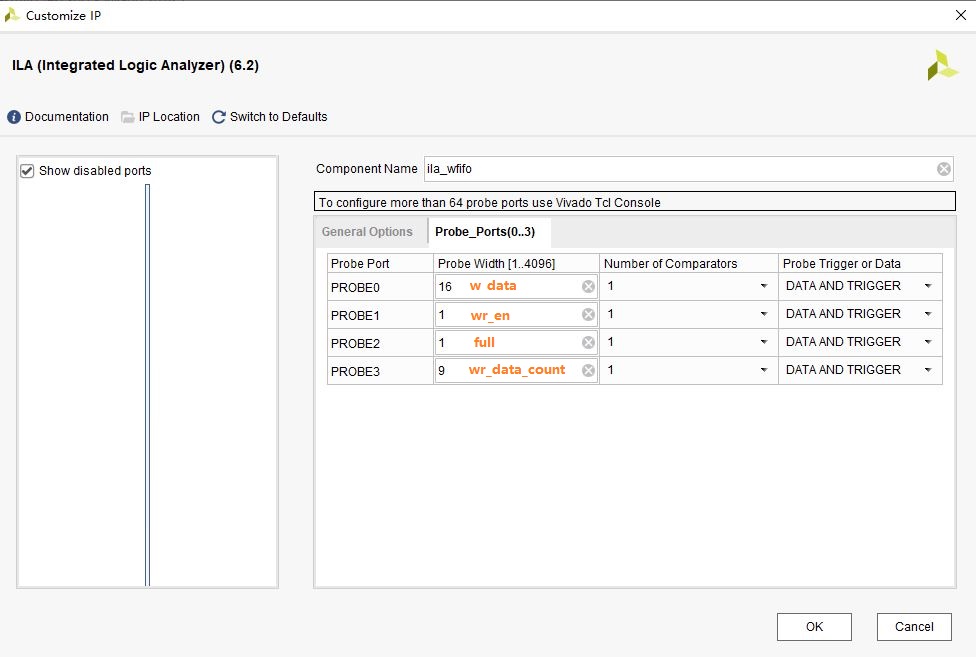
The corresponding codes are as follows.
reg	 [15:0] 		w_data			;	   		//FIFO write data
wire      			wr_en			;	   		//FIFO write enable
wire       			full			;  			//FIFO full signal
wire [8:0]  		wr_data_count	;  			//Number of data written
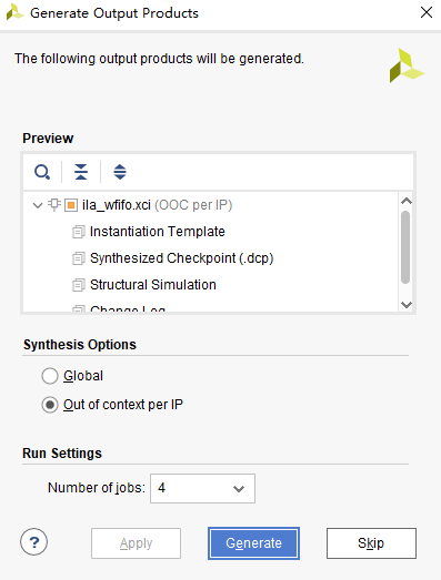
Click OK to pop up the following dialog box. Click Generate to Generate the ILA IP core of the write channel.
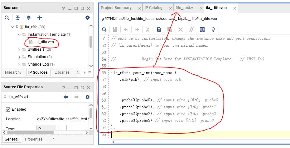
Next, add the ILA IP core of the read channel, as shown in the figure below.

Set the number of bits for each read channel probe according to the code, as shown in the figure below.
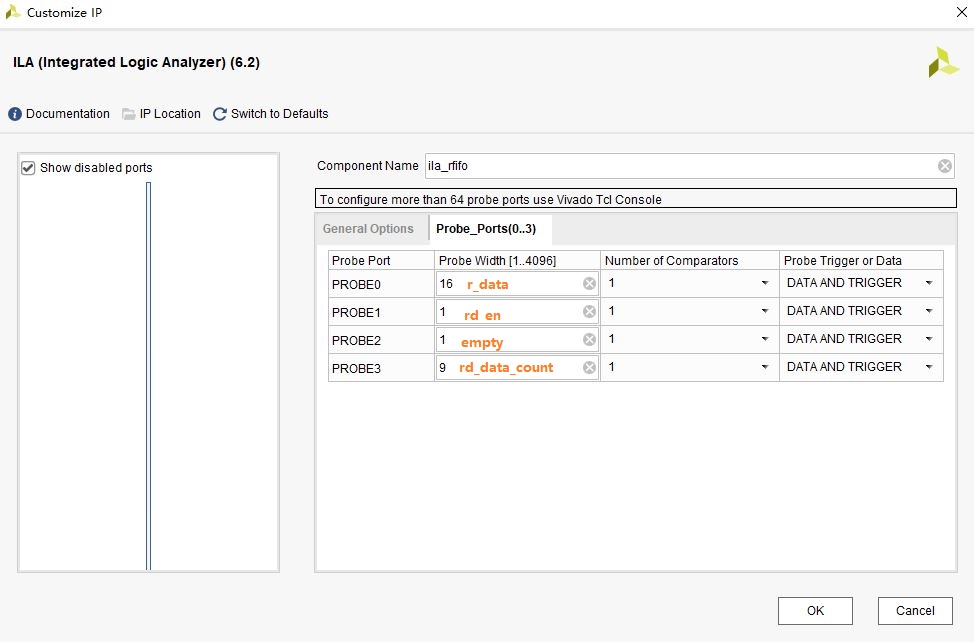
The corresponding codes are as follows.
wire [15:0] 		r_data			;			//FIFO read data
wire      			rd_en			;	   		//FIFO read enable
wire       			empty			;  			//FIFO null signal
wire [8:0]  		rd_data_count	;  			//Number of readable data
Click OK to pop up the following dialog box. Click Generate to Generate the ILA IP core of the read channel.
5, Write test program
Create a new file named FIFO_ The Verilog file of test can be carried out according to the sequence number marked in the figure below.
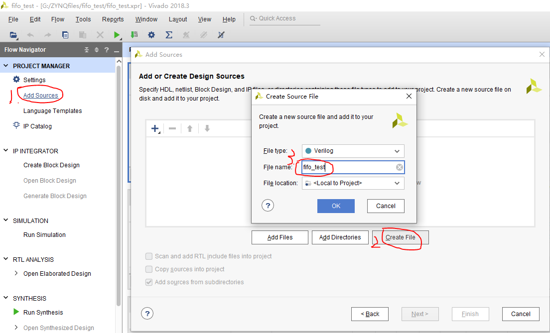
Create a new FIFO_ test. Write the following code in V.
//The code comes from the punctual atom
`timescale 1ns / 1ps

module fifo_test
	(
		input 		clk,		         //50MHz clock
		input 		rst_n	             //Reset signal, active at low level
	);

reg	 [15:0] 		w_data			;	   		//FIFO write data
wire      			wr_en			;	   		//FIFO write enable
wire      			rd_en			;	   		//Read enable FIFO
wire [15:0] 		r_data			;			//FIFO read data
wire       			full			;  			//FIFO full signal
wire       			empty			;  			//FIFO null signal
wire [8:0]  		rd_data_count	;  			//Number of readable data
wire [8:0]  		wr_data_count	;  			//Number of data written

wire				clk_100M 		;			//PLL generates 100MHz clock
wire				clk_75M 		;			//PLL generates 100MHz clock
wire				locked 			;			//PLL lock signal can be used as system reset signal, and high level indicates lock
wire				fifo_rst_n 		;			//fifo reset signal, active at low level

wire				wr_clk 			;			//Write FIFO clock
wire				rd_clk 			;			//Read FIFO clock
reg	[7:0]			wcnt 			;			//Wait for counter after write FIFO reset
reg	[7:0]			rcnt 			;			//Wait for counter after reading FIFO reset

//Instantiate PLL to generate 100MHz and 75MHz clocks
clk_wiz_0 fifo_pll
 (
  // Clock out ports
  .clk_out1(clk_100M),     	 	// output clk_out1
  .clk_out2(clk_75M),    		// output clk_out2
  // Status and control signals
  .reset(~rst_n), 			 	// input reset
  .locked(locked),       		// output locked
  // Clock in ports
  .clk_in1(clk)					// input clk_in1
  );

assign fifo_rst_n 	= locked	;	//Assign the LOCK signal of PLL to the reset signal of fifo
assign wr_clk 		= clk_100M 	;	//Assign 100MHz clock to write clock
assign rd_clk 		= clk_75M 	;	//Assign 75MHz clock to read clock

/* Write FIFO state machine */
localparam      W_IDLE      = 1	;
localparam      W_FIFO     	= 2	;

reg[2:0]  write_state;
reg[2:0]  next_write_state;

always@(posedge wr_clk or negedge fifo_rst_n)
begin
	if(!fifo_rst_n)
		write_state <= W_IDLE;
	else
		write_state <= next_write_state;
end

always@(*)
begin
	case(write_state)
		W_IDLE:
			begin
				if(wcnt == 8'd79)               //Wait for a certain time after reset. The slowest clock in safety circuit mode is 60 cycles
					next_write_state <= W_FIFO;
				else
					next_write_state <= W_IDLE;
			end
		W_FIFO:
			next_write_state <= W_FIFO;			//Always writing FIFO status
		default:
			next_write_state <= W_IDLE;
	endcase
end
//In the IDLE state, that is, after reset, the counter counts
always@(posedge wr_clk or negedge fifo_rst_n)
begin
	if(!fifo_rst_n)
		wcnt <= 8'd0;
	else if (write_state == W_IDLE)
		wcnt <= wcnt + 1'b1 ;
	else
		wcnt <= 8'd0;
end
//In the write FIFO state, if not satisfied, write data to the FIFO
assign wr_en = (write_state == W_FIFO) ? ~full : 1'b0;
//When the write enable is valid, the write data value is increased by 1
always@(posedge wr_clk or negedge fifo_rst_n)
begin
	if(!fifo_rst_n)
		w_data <= 16'd1;
	else if (wr_en)
		w_data <= w_data + 1'b1;
end

/* Read FIFO state machine */
localparam      R_IDLE      = 1	;
localparam      R_FIFO     	= 2	;
reg[2:0]  read_state;
reg[2:0]  next_read_state;

//Generate FIFO read data
always@(posedge rd_clk or negedge fifo_rst_n)
begin
	if(!fifo_rst_n)
		read_state <= R_IDLE;
	else
		read_state <= next_read_state;
end

always@(*)
begin
	case(read_state)
		R_IDLE:
			begin
				if (rcnt == 8'd59)             	//Wait for a certain time after reset. The slowest clock in safety circuit mode is 60 cycles
					next_read_state <= R_FIFO;
				else
					next_read_state <= R_IDLE;
			end
		R_FIFO:
			next_read_state <= R_FIFO ;			//Always reading FIFO status
		default:
			next_read_state <= R_IDLE;
	endcase
end

//In the IDLE state, that is, after reset, the counter counts
always@(posedge rd_clk or negedge fifo_rst_n)
begin
	if(!fifo_rst_n)
		rcnt <= 8'd0;
	else if (write_state == W_IDLE)
		rcnt <= rcnt + 1'b1 ;
	else
		rcnt <= 8'd0;
end
//In the state of reading FIFO, if it is not empty, read data from FIFO
assign rd_en = (read_state == R_FIFO) ? ~empty : 1'b0;

//Instantiate FIFO
fifo_ip fifo_ip_inst
(
  .rst            (~fifo_rst_n    	),   // input rst
  .wr_clk         (wr_clk          	),   // input wr_clk
  .rd_clk         (rd_clk          	),   // input rd_clk
  .din            (w_data       	),   // input [15 : 0] din
  .wr_en          (wr_en        	),   // input wr_en
  .rd_en          (rd_en        	),   // input rd_en
  .dout           (r_data       	),   // output [15 : 0] dout
  .full           (full         	),   // output full
  .empty          (empty        	),   // output empty
  .rd_data_count  (rd_data_count	),   // output [8 : 0] rd_data_count
  .wr_data_count  (wr_data_count	)    // output [8 : 0] wr_data_count
);

//Write channel logic analyzer
ila_wfifo ila_wfifo (
	.clk		(wr_clk			),
	.probe0		(w_data			),
	.probe1		(wr_en			),
	.probe2		(full			),
	.probe3		(wr_data_count	)
);
//Read channel logic analyzer
ila_rfifo ila_rfifo (
	.clk		(rd_clk			),
	.probe0		(r_data			),
	.probe1		(rd_en			),
	.probe2		(empty			),
	.probe3		(rd_data_count	)
);

endmodule
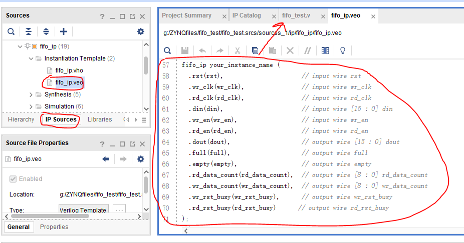
The code of instantiating FIFO comes from FIFO_ FIFO in IP_ ip. VEO file, but the parameters in parentheses need to be modified.
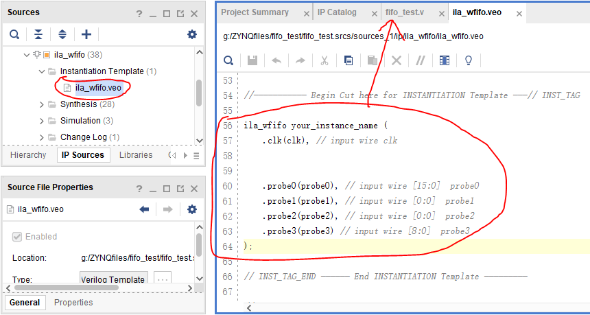
The code of instantiating write channel ila logic analyzer comes from ila_ ila in wfifo_ wfifo. VEO file, but the parameters in parentheses need to be modified.
The code of instantiating the reading channel ila logic analyzer comes from ila_ ila in rfifo_ rfifo. VEO file, but the parameters in parentheses need to be modified.
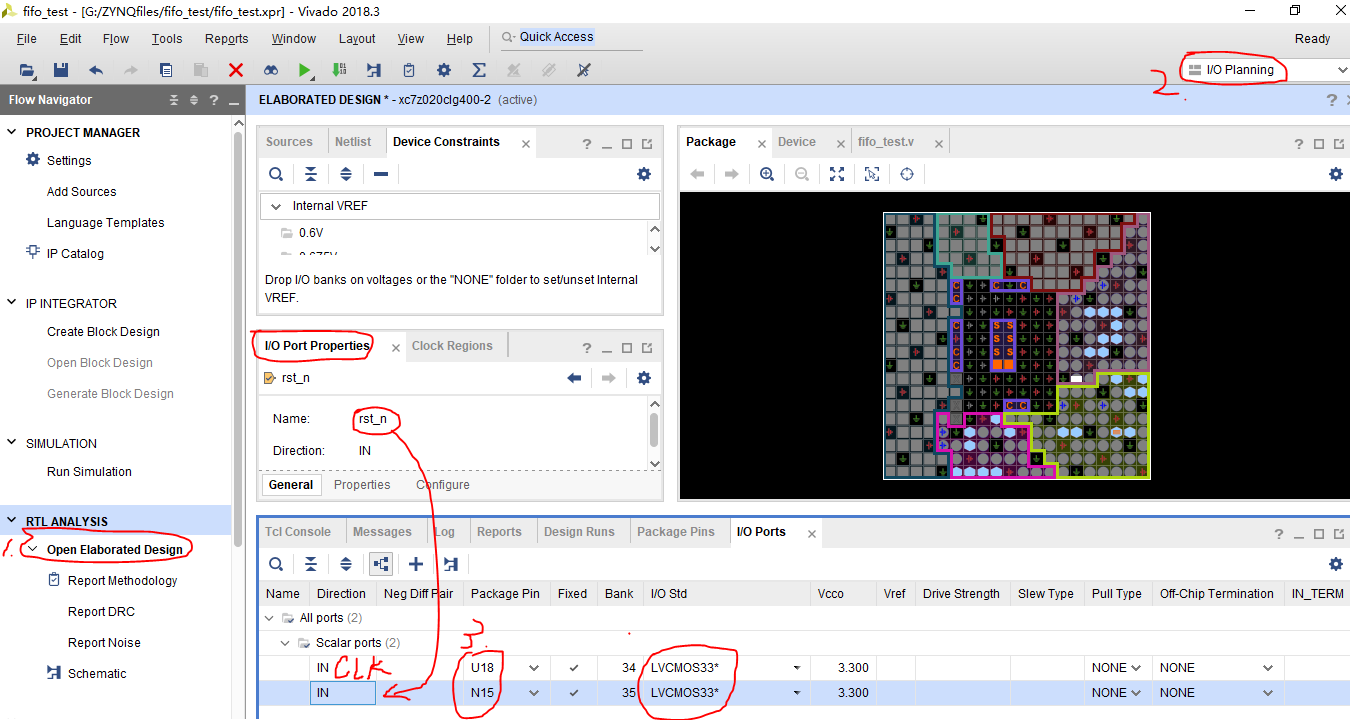
6, Allocation pin
In this experiment, only clock signal CLK (pin U18) and reset signal RST need to be allocated pins_ N (the pin is N15), the pin allocation can be completed according to the numerical order in the figure below.
After pin assignment is completed, Ctrl+S saves and the name is consistent with the project name.
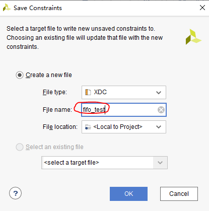
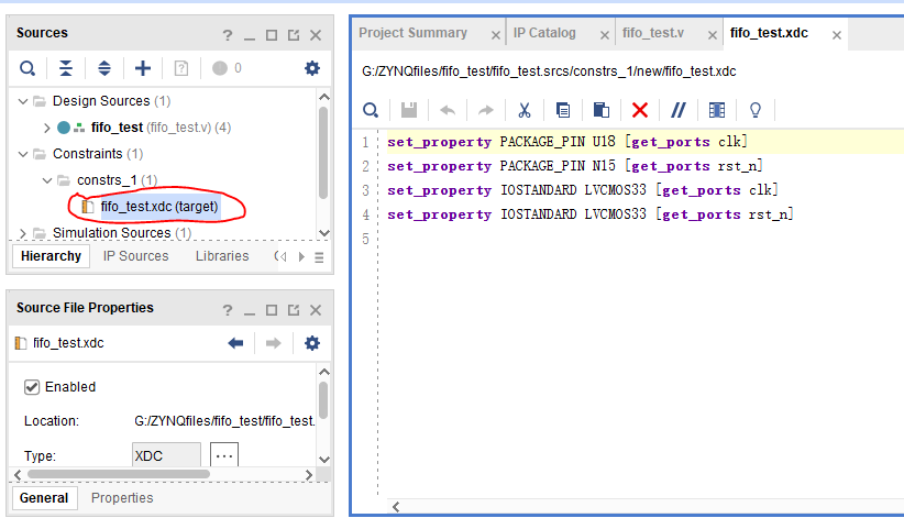
Pin assignment information in fifo_test.xdc file.
7, Simulator simulation
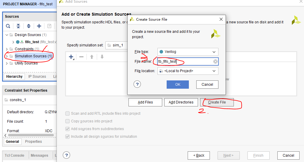
Right click Simulation Sources and select Add Source to create a new TB file according to the sequence number in the figure below.
In TB_ fifo_ test. Write the following code in the V file.
//The code comes from the punctual atom
`timescale 1ns / 1ps

module vtf_fifo_tb;
// Inputs
reg clk;
reg rst_n;

// Instantiate the Unit Under Test (UUT)
fifo_test uut (
	.clk	(clk),
	.rst_n		(rst_n)
);

initial
begin
	// Initialize Inputs
	clk = 0;
	rst_n = 0;

	// Wait 100 ns for global reset to finish
	#100;
      rst_n = 1;

 end

always #10 clk = ~ clk;   // A cycle of 20ns generates a 50MHz clock source

endmodule
After saving the code, select Run Simulation under SIMULATION and select the first behavior SIMULATION.
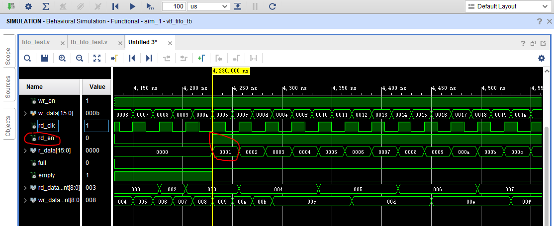
Drag the signals defined in all codes into the waveform simulation window, set the simulation time to 10us, and the results after operation are shown in the figure below.
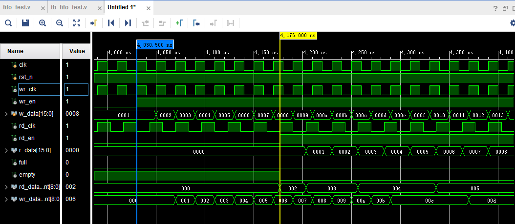
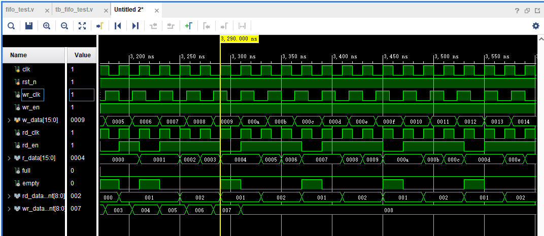
As can be seen from the simulation results, write enable WR_ When en is valid, start to write data. The initial value is 0001. When writing empty from the beginning, it needs a certain period, because there is also synchronization processing inside. After it is not empty, start reading data, and the read data is relative to rd_en lags by one cycle.
Extend the simulation cycle to 100us. If the FIFO is full, no data will be written to the FIFO according to the program design, wr_en also pulled down.
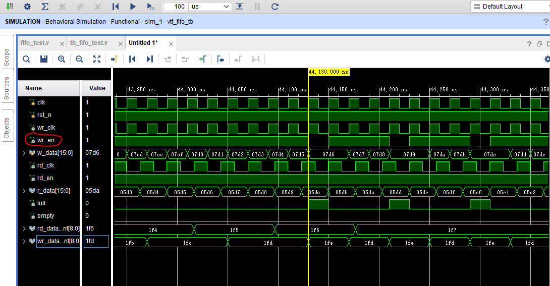
The reason why FIFO is full is that the write clock is faster than the read clock. If the write clock is exchanged with the read clock, that is, the read clock is faster, it will be empty.
Exchange read-write clock cycles and simulate again.
The simulation results are shown in the figure below.
Change the Read Mode of FIFO to First Word Fall Through, and then conduct simulation.
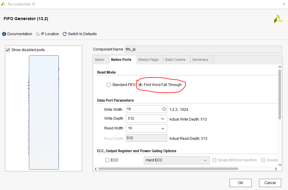
The simulation results are shown in the figure below. It can be seen that RD_ When en is valid, the data is also valid without a cycle difference. This is the difference between the First Word Fall Through simulation mode and Standard FIFO.
That is, in the First Word Fall Through read mode, FIFO will take out a data in advance. When the read signal is valid, the corresponding data is also valid.
8, Hardware debugging
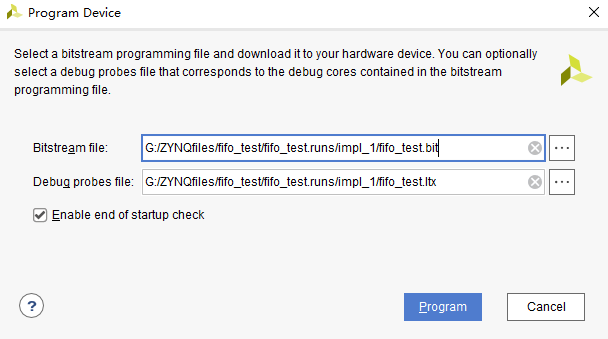
Connect the development board, click Generate Bitstream to Generate Bitstream file and download it to the development board.
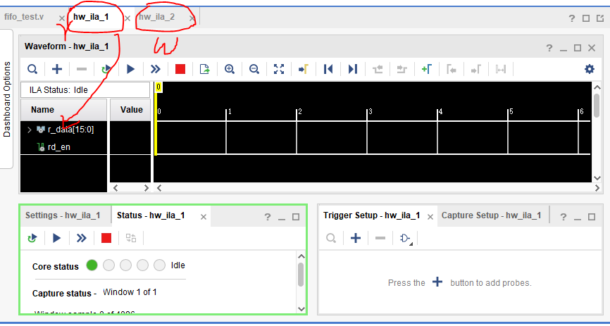
At this time, two ila documents will be generated, corresponding to read channel and write channel respectively.
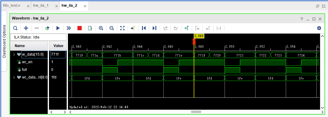
Let's first look at the write channel. The corresponding file is hw_ila_2. The simulation results are shown in the figure below. It can be seen that the full signal is high, wr_en is low level, and FIFO no longer writes data to it.
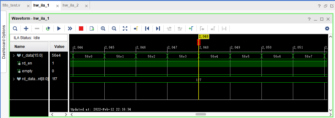
Try the read channel again. The corresponding file is hw_ila_1. The simulation results are shown in the figure below.
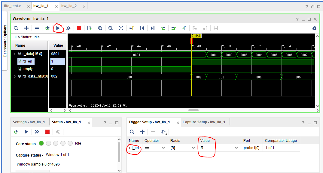
If in RD_ The rising edge of en is used as the trigger condition, click Run, and then press the reset button, that is, the PL KEY1 button on the development board. The following results will appear, which is consistent with the simulation results. Under the standard FIFO mode, the data lag is Rd_ One cycle.
summary
The above is all the contents of the FPGA on-chip FIFO read-write test experiment of ZYNQ. The experimental process is basically similar to the experimental process of FPGA on-chip RAM and ROM read-write test, but there are also obvious differences. This experiment adds PLL IP core and two ILA logic analyzers. These are more complex than the previous experiments. We should learn this hardware test method, In order to be applied in subsequent experiments.
Reference: punctual atom - course_s1_ZYNQ those things - FPGA experiment v1 06.pdf