IIC
Inter integrated circuit
The serial bus is composed of data line SDA and clock line SCL, which can send and receive data.
SCL: plays a control role in communication.
SDA: bit transfer data.
Software IIC: through the I/O port simulation of single chip microcomputer, use software to control I/O port to simulate communication waveform, and software to simulate the working mode of register.
Hardware IIC: through the IIC drive circuit, the hardware directly calls the register configuration.
Half duplex communication mode
IIC communication protocol
It mainly includes the processes of start, end, sending, response and receiving.
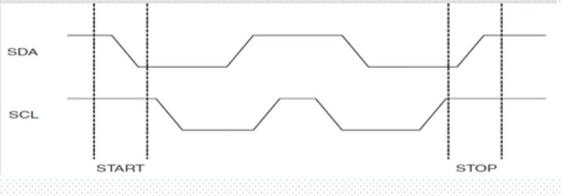
//Generate IIC start signal
//1. Set SDA output
//2. First pull up SDA, then SCL, idle state
//3. Lower SDA
//4. Prepare to receive data
void IIC_Start(void)
{
    SDA_OUT();     //sda line output
    IIC_SDA=1;
    IIC_SCL=1;
    delay_us(4);
     IIC_SDA=0;//START:when CLK is high,DATA change form high to low
    delay_us(4);
    IIC_SCL=0;//Clamp the I2C bus and prepare to send or receive data
}
//Generate IIC stop signal
//1. Set SDA output
//2. Lower SDA first and then SCL
//3. Raise SCL
//4. Pull up SDA
//5. Stop receiving data
void IIC_Stop(void)
{
    SDA_OUT();//sda line output
    IIC_SCL=0;
    IIC_SDA=0;//STOP:when CLK is high DATA change form low to high
     delay_us(4);
    IIC_SCL=1;
    IIC_SDA=1;//Send I2C bus end signal
    delay_us(4);
}
Response signal
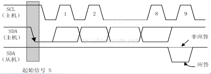
Each time the master sends a byte of data to the slave, the master needs to wait for the slave to send a response signal to determine whether the slave has received data. The clock required by the slave is provided by the master. The response is in the clock cycle after completing 8 data bits. Low level 0 is the response and 1 is the non response.
Response procedure:
//Generate ACK response
//It is clear here to generate response: SCL completes low-level and high-level conversion during SDA is always low-level
void IIC_Ack(void)
{
    IIC_SCL=0;
    SDA_OUT();
    IIC_SDA=0;
    delay_us(2);
    IIC_SCL=1;
    delay_us(2);
    IIC_SCL=0;
}
//No ACK response is generated
//It is clear here that no response is generated: SCL completes low-level and high-level conversion while SDA is always high-level
void IIC_NAck(void)
{
    IIC_SCL=0;
    SDA_OUT();
    IIC_SDA=1;
    delay_us(2);
    IIC_SCL=1;
    delay_us(2);
    IIC_SCL=0;
}
Send data:
void IIC_Send_Byte(u8 txd)
{
    u8 t;
    SDA_OUT();
    IIC_SCL=0;//Pull down the clock to start data transmission
    for(t=0;t<8;t++)
    {
        //IIC_SDA=(txd&0x80)>>7;
        //Get the highest bit of the data and move it 7 bits left
        //If a bit is 1, SDA is 1, otherwise it is the opposite
        if((txd&0x80)>>7)
            IIC_SDA=1;
        else
            IIC_SDA=0;
        txd<<=1;
        delay_us(2);   //These three delays are necessary for TEA5767
        IIC_SCL=1;
        delay_us(2);
        IIC_SCL=0;
        delay_us(2);
    }
}
After sending a byte, the MCU must be followed by an external response function:
Idea: first let SDA=1, and then judge whether SDA becomes 0 within a certain time, so as to identify whether the peripheral has sent a response signal.
u8 IIC_Wait_Ack(void)
{
    u8 ucErrTime=0;
    SDA_IN();      //SDA set as input
    IIC_SDA=1;delay_us(1);
    IIC_SCL=1;delay_us(1);
    while(READ_SDA)
    {
        ucErrTime++;
        if(ucErrTime>250)
        {
            IIC_Stop();
            return 1;
        }
    }
    IIC_SCL=0;//Clock output 0
    return 0;
}
receive data
The transmitted data is transmitted through bit, the received data is received through bit, and finally the response signal is returned:
u8 IIC_Read_Byte(unsigned char ack)
{
    unsigned char i,receive=0;
    SDA_IN();//SDA set as input
    for(i=0;i<8;i++ )
    {
        IIC_SCL=0;
        delay_us(2);
        IIC_SCL=1;
        receive<<=1;
        if(READ_SDA)receive++;
        delay_us(1);
    }
    if (!ack)
        IIC_NAck();//Send nACK
    else
        IIC_Ack(); //Send ACK
    return receive;
}
SPI
Serial Peripheral interface
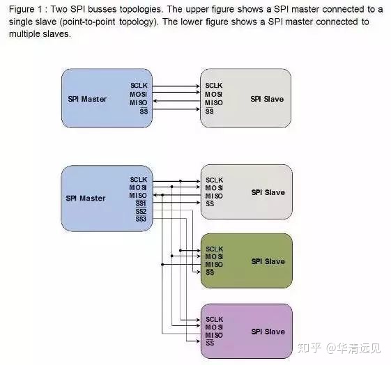
- SCLK: Serial Clock (output from master); Serial clock (host output)
- MOSI; SIMO: Master Output, Slave Input(output from master); Master output, slave input (slave output)
- MISO; SOMI: Master Input, Slave Output(output from slave); Master input, slave output (slave output)
- SS: Slave Select (active low, outputfrom master). Slave selection (active low level, host output)
SPI is a high-speed, full duplex, synchronous communication bus, and only occupies four wires on the pins of the chip
The clock polarity CPOL is used to configure which state the SCLK level is in the idle state or the active state, and the clock phase CPHA is used to configure which edge the data sampling is on:
- CPOL=0 means that SCLK is in idle state when SCLK=0, so the effective state is that SCLK is at high level;
- CPOL=1 indicates that SCLK is in idle state when SCLK=1, so the effective state is that SCLK is at low level;
- CPHA=0, indicating that the data is sampled at the first edge and the data is sent at the second edge;
- CPHA=1, indicating that data sampling is at the second edge and data transmission is at the first edge.
Under the control of SCLK, the data is moved out of the master register and slave register from high to low, and into the slave register and master register in turn** When all the contents of the register are moved out, the exchange of the contents of the two registers is completed.