Salty spoon design
1, Overview
Hot pot, barbecue, crayfish, people always want to eat something to satisfy their appetite at night. In addition to being delicious, these heavy taste things also contain very high salt, sugar and oil. Among them, high salt food is almost everywhere, and people with long-term high salt diet are prone to hypertension, cardiovascular disease and so on. In order to let us enjoy delicious food while avoiding these health hazards, we came up with a salty spoon to solve it.
The principle of salty spoon is actually very simple. When humans eat, the taste buds of the tongue will produce corresponding bioelectricity, which will be transmitted to the brain to let everyone know the taste. Similarly, if we use the stimulation of low-frequency current of 20-50uA, it will also produce the effect of actually tasting food.
This article will take the salty spoon as a reference to introduce you how to make a spoon with taste. You can also design other flavors according to your preferences.
| taste | Current & temperature parameters |
|---|---|
| salty | Low frequency current of 20-50uA |
| acid | The current and tongue temperature of 60-180uA rise from 20 ℃ to 30 ℃ |
| sweet | The reverse current and tongue temperature rise to 35 ℃ first, and then slowly decrease to 20 ℃ |
| bitter | Reverse current of 60-140uA |
| hot | The temperature is heated from 33 ℃ to 38 ℃ |
| mint | The temperature decreased from 22 ℃ to 19 ℃ |
2, Introduction to hardware scheme
1. Hardware block diagram

2. Hardware design
(1) Schematic diagram( Click download)

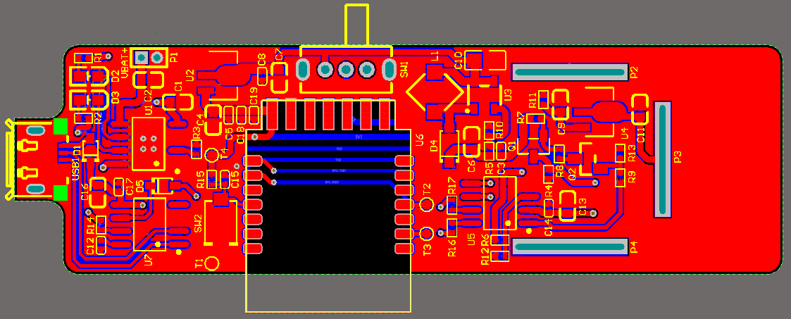
(2) PCB diagram( Click download)
3. Circuit function
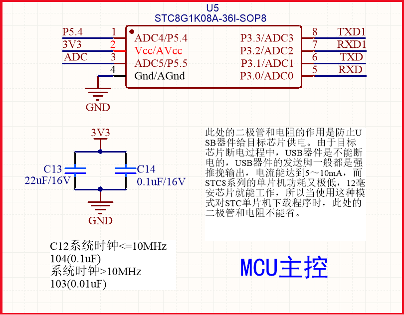
(1) MCU main control circuit
MCU master chip selection STC A single chip microcomputer with simple peripheral circuit and low power consumption.
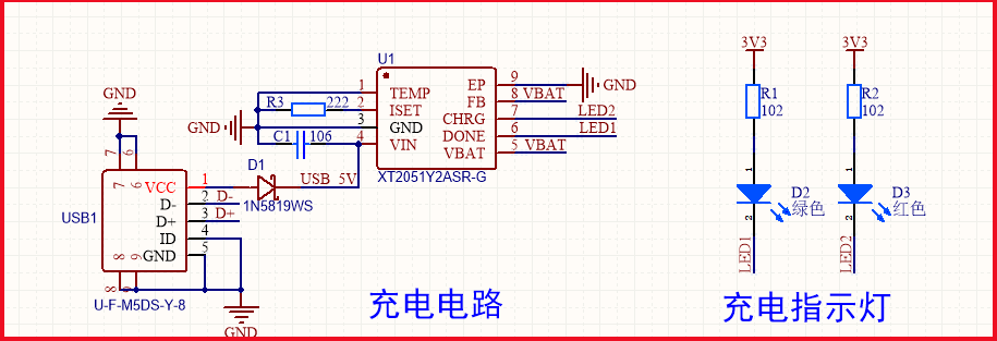
(2) Power management circuit
Charging management circuit: XT2051 It is a constant current / constant voltage charging circuit for single-cell lithium-ion battery. The device includes an internal power transistor, which does not require external current detection resistors and blocking diodes in applications. XT2051 requires a minimum of external components and meets the USB bus specification. And low power consumption, low cost, very suitable for portable, battery powered applications.
(3) Boost control circuit

Output voltage calculation: VOUT=1.233*(1+R5/R10) is about 8V.
The selection of inductance value determines the maximum switching frequency of the converter, and the inductance value should have a saturation current that meets the maximum peak current of the converter.
Ipeak(typ)=400ma+Vin/L*100ns. The smaller the inductor value, the higher the chip switching frequency, but the lower the efficiency. The inductance value has little effect on the available current of the maximum load, which is only secondary (as can be seen from the calculation formula in the chip manual). The range of inductance value is 2.2uH~47uH.
It is necessary to provide sufficient overspeed drive for the error comparator through the feedforward capacitor of the feedback resistor R5. If there is no feedforward capacitance or the feedforward capacitance is too small, TPS61040 On the switch node (SW), double pulse or pulse burst is displayed instead of single pulse, resulting in higher output voltage ripple. If this higher output voltage ripple is acceptable, the feedforward capacitor can be excluded. The lower the switching frequency of the frequency converter, the greater the feedforward capacitance required. The required value of feedforward capacitance at the operating point can also be calculated by the following formula: C3=1/(23.14(fs/20)*R5)
Methods to improve line supervision: 1. Use a smaller inductance value to increase the switching frequency, which will reduce the output voltage ripple and the voltage ripple on the feedback pin. 2. 2. Add a small capacitor from the feedback pin (FB) to the ground to reduce the voltage ripple on the feedback pin to 50mv. As a starting point, the same capacitance value as the feedforward capacitance C3 can be used.
(4) Low frequency constant current source circuit
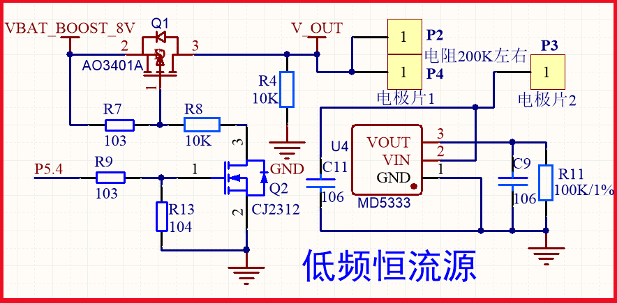
MCU IO output PWM wave is used to control the frequency of current.
utilize LDO It is a constant current source based on the function of module voltage stabilization and the characteristic that the input current is equal to the output current.
Iout=Vout/R11=3.3V/100K=33uA.
Current and frequency meet the human body's feeling of saltiness at the same time.
(5) Wireless communication control circuit
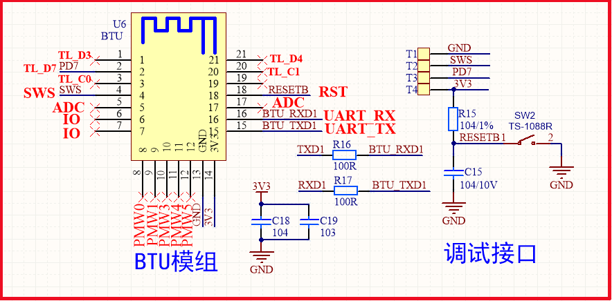
Design of a low power embedded BLE protocol based on graffiti intelligence for wireless communication BTU Module.
3, Appearance and structure design
After the circuit analysis, let's take a look at the shape and structure of the spoon. The shape and structure of the spoon is also a crucial part. How to make the spoon portable, exquisite and compact still needs the imagination of developers. In the structure, a spoon, an electrode sheet embedded in the structure and a human tongue are used to form a circuit, so that the current flows from the human body to the tongue. Electrode pieces and spoons need to be conductive materials.

4, Product creation
This demo is developed based on graffiti IoT platform. There are no Baiwei spoon products in the existing categories. Therefore, click to find the category. Fill in the product name, product description and communication protocol in turn, and select Bluetooth. The BLE module is used for development, and the device is paired and controlled through Bluetooth in the graffiti APP.

5, Firmware development
(1) Serial port initialization and function
void UartInit()		//9600bps@11.0592MHz
{
	P_SW1 &= ~(3<<6);
	P_SW1 |= 1<<6;			//RXD/P3.2, TXD/P3.3
	P3M0 |= 1<<3;
	P3M1 &= ~(1<<3); //TX push pull output
	SCON = 0x50;		//8-bit data, variable baud rate
	AUXR |= 0x40;		//Timer clock 1T mode, no frequency division
	AUXR &= 0xFE;		//Serial port 1 selects timer 1 as baud rate generator
	TMOD &= 0x0F;		//Set timer mode
	TL1 = 0xE0;		//Set timing initial value
	TH1 = 0xFE;		//Set timing initial value
	ET1 = 0;		//Disable timer 1 interrupt
	ES=1;						//Open receive interrupt
	TR1 = 1;		//Timer 1 starts timing
}

void Uart_PutChar(unsigned char value)
{
	SBUF=value;//Put the received data into the transmit register
	while(!TI);			 //Wait for sending data to complete
	TI=0;						 //Clear the transmission completion flag bit
}

void Usart() interrupt 4
{
	u8 receiveData;
	receiveData=SBUF;//Data received
	RI = 0;//Clear receive interrupt flag bit
	uart_receive_input(receiveData);
}
(2) Timer initialization and function
void Timer0Init()		//1000 microseconds @ 11.0592MHz
{
	P5M0 |=1<<4;
	P5M1 &=~(1<<4);	//P54 output mode
	AUXR |= 0x80;		//Timer 0 clock 1T mode
	TMOD &= 0xF0;		//Set timer mode
	TL0 = 0xCD;		//Set timing initial value
	TH0 = 0xD4;		//Set timing initial value
	TF0 = 0;		//Clear TF0 flag
	ET0=1;//Enable timer 0 interrupt
	EA=1;//Open total interrupt
	TR0 = 1;		//Timer 0 starts timing
}

void Timer0() interrupt 1
{
	static u16 i=0;
	static u16 count=0;
	if(fre_set>=100)//Frequency greater than or equal to 100Hz
	{
		TL0 = (65535-11059/fre_set*500)%256;
		TH0 = (65535-11059/fre_set*500)/256;
		i=0;
		P54 =~P54;
		count++;
	}
	else if(fre_set<100)//0.1ms
	{
		TL0 = 0xAE;		//Set timing initial value
		TH0 = 0xFB;		//Set timing initial value
		if(fre_set==0)
		{
			P54=1;
		}
		else
		{
			i++;
			if(i>(5000/fre_set))
			{
				P54 =~P54;
				i=0;
				count++;
			}
		}
	}
	if(count>(4*fre_set))
	{
		count=0;
		f_task_ad=1;
	}
}
(3) ADC initialization and function
void ADCInit()
{
    P5M0 &= ~(1<<5);                                //Set P5 5 is ADC port
    P5M1 |= 1<<5;
    P_SW2 |= 0X80;
    ADCTIM=0X3F;
    P_SW2 &= 0X7F;
    ADCCFG |= 0x0f;                              //Set ADC clock to system clock / 2 / 16 / 16
    ADC_CONTR |=5;  													//Set channel 5
    ADC_CONTR |= 0x80;                           //Enable ADC module
}

void TASK_ADC()		//1000 microseconds @ 11.0592MHz
{
	ADC_CONTR |= 0x40;                      //Start AD conversion
	while (!(ADC_CONTR & 0x20)) ;           //Query ADC completion flag
    _nop_();
	_nop_();
	ADC_CONTR &= ~0x20;                     //Cleaning completion mark
	voltage = ADC_RES*4+ADC_RESL/64;                           //Read ADC results
	voltage = voltage *32/5;
	mcu_dp_value_update(DPID_VOLTAGE,voltage);//Report
}
6, Summary
With the smart spoon in your hand and the graffiti smart APP, let's explore those unknown delicacies. Graffiti IoT development platform provides developers with convenient IoT development tools and services, helps developers complete device access more efficiently, and provides developers with IoT application development and scene service capabilities.