Introduction to DSP: Interrupt PIE
1. The interrupt management of DSP is divided into three levels: peripheral level, PIE level and CPU level.
Among them, peripheral interrupt management is responsible for the permission and prohibition of specific peripheral interrupt sources, PIE interrupt management is responsible for grouping peripheral interrupts and managing them according to priority, and CPU kernel interrupt management is responsible for processing interrupt requests directly to the CPU. 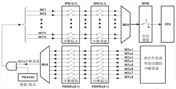
The peripheral interrupt extension module (PIE) of the DSP controller extends the interrupt centrally so that each level of CPU interrupt can respond to multiple interrupt sources.
2. PIE level interruption and management:
CPU kernel level interrupts (INT1-INT14) and INT1-INT12 are used by PIE module for interrupt extension. There are 12 groups with 8 interrupt sources in each group.
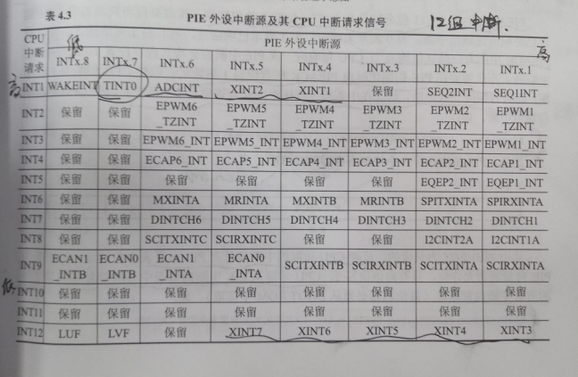
The priority of each interrupt decreases gradually from right to left. The overall priority of INT1 is the highest and INT12 is the lowest.
INT13 is multiplexed by CPU timer 1 and external interrupt XINT13, and INT14 is exclusively owned by timer 2.
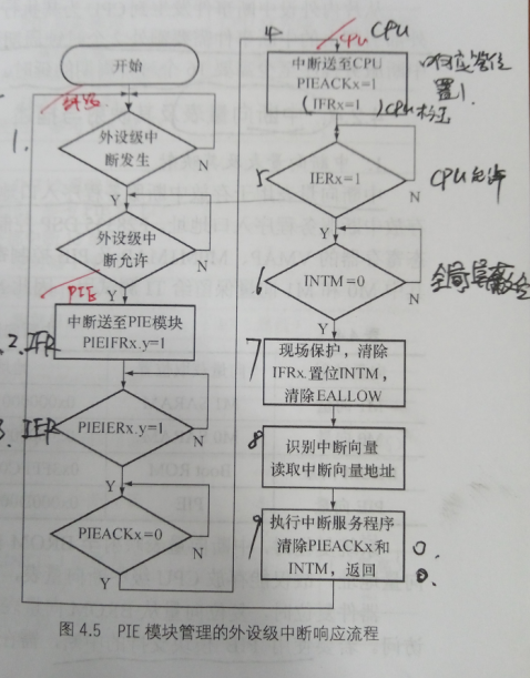
3. Interruption response process
4. Interrupt Register Introduction
- PIEIFRx (1-12) interrupt flag register
- PIEIERx (1-12) Interrupt Shielding Register
Each has 12 bits, each 16 bits wide, and only the first 8 bits are used to represent 8 interrupt sources respectively; IFR flags interrupt arrival, and IER indicates whether to respond (PIEIFRx.1-8, PIEIERx.1-8) - PIEACKx (1-12) Response Points
Whether the CPU responds to the bit-given interrupt, feeds the 0 interrupt to the CPU, and waits for the 1 interrupt PIECTRL PIE Control Register, Read Only
Read interrupt vectorsXINTnCR (n 1-7) 7 external interrupts
Select interrupt edge, 01 rising edge; external interrupt allowable bit
5. Code slice
PieCtrlRegs.PIEIFR1.bit.INTx4=1;//Setting the interrupt flag bit of XINT 1 in PIE interrupt group 1
PieCtrlRegs.PIEIER1.bit.INTx4=1;//XINT1 interrupt allowed for PIE interrupt group 1

PieCtrlRegs.PIEACK.all = 0x0004;//Clear the ACK bit of interrupt group 3 to respond again
PieCtrlRegs.PIECTRL.bit.ENPIE=1;//Read interrupt vectors from vector tables- 1
- 2
- 3
- 4
- 5
6. Examples of timer interruption
#include "DSP2833x_Device.h"
#include "DSP2833x_Examples.h"

interrupt void cpu_timer0_isr(void);//Declare interrupt service functions

void main()
{

    //Step 1: Initialize system control, PLL, watchdog, allowable peripheral clock
    InitSysCtrl();

    //Step 2: Initialize GPIO
    InitGpio();

    //Step 3: Clear all interrupts and initialize PIE vector table
    DINT;
    InitPieCtrl();   //Initialize PIE Controller
    IER = 0x0000;    //Prohibit CPU interruption
    IFR = 0x0000;    //Clear all CPU interrupt flags
    InitPieVectTable();   //Initialize PIE interrupt vector table

    EALLOW;
    PieVectTable.TINT0 = &cpu_timer0_isr;   //Remap the interrupt vector to the interrupt service program
    EDIS;

    //Step 4: Initializing peripheral modules
    InitCpuTimers();
    ConfigCpuTimer(&CpuTimer0,150,1000000);  //150 MHz, cycle 1 second
    CpuTimer0Regs.TCR.all = 0x4001;          //Allow timer interrupt and set TSS to 0 to start timer work

    //step5:
    IER |= M_INT1;                          //Allow CPU INT1 interruption, which connects to TINT0
    PieCtrlRegs.PIEIER1.bit.INTx7 = 1;      //TINT0 interrupt allowed in PIE interrupt group 1
    EINT;           //Clear global shielding
    ERTM;           //Allow global real-time interruption

    //step6: cycle
    while(1);


}


interrupt void cpu_timer0_isr(void)
{
    CpuTimer0.InterruptCount++;
    PieCtrlRegs.PIEACK.all = PIEACK_GROUP1;   //Clear the response bit of PIE interrupt group 1 so that the CPU can respond again

}
- 1
- 2
- 3
- 4
- 5
- 6
- 7
- 8
- 9
- 10
- 11
- 12
- 13
- 14
- 15
- 16
- 17
- 18
- 19
- 20
- 21
- 22
- 23
- 24
- 25
- 26
- 27
- 28
- 29
- 30
- 31
- 32
- 33
- 34
- 35
- 36
- 37
- 38
- 39
- 40
- 41
- 42
- 43
- 44
- 45
- 46
- 47
- 48
- 49
- 50
- 51
- 52
7. Example of External Interruption
Follow-up examples, first occupy a pit
- 1