1. Basic principles
In fact, driving the LCD is to write data to the LCD display memory. The place where 1 is written is displayed, and the place where 0 is written is not displayed. The reverse display is just the opposite; Since the video memory is distributed in 128 columns and 64 rows, it is also called 12864 liquid crystal.
2. Basic characteristics
Working voltage 3.3V, backlight voltage 3.0VMA communication mode;
8-bit parallel (6800 and 8080 timing), 4-wire serial communication 12864;
Memory of dot matrix display (DDRAM is 13265);
Display contrast, internal register adjustment (software adjustment contrast);
Duty ratio 1 / 64, bias ratio 1 / 9;
Operating temperature - 20 to + 70 degrees.
3. Video memory mapping
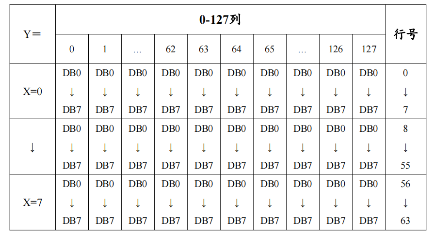
It can be seen that the column is defined as 0-127, and the row address range is defined as (0-7) pages in units of 8 pixels, a total of 64.
4. Pin description
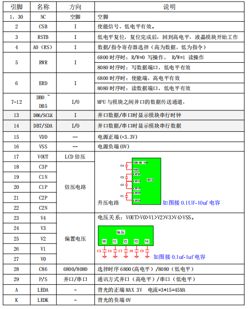
It can be seen that the high and low level of pin 29 determines whether to use parallel port or serial port.
5. Serial mode drive timing
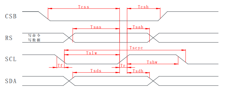
As can be seen from the figure:
Data or command transmission when CSB is pulled low;
Transmit data when RS is high, and transmit instructions when RS is low;
SCL is the clock;
SDA is data.
6. Serial write process
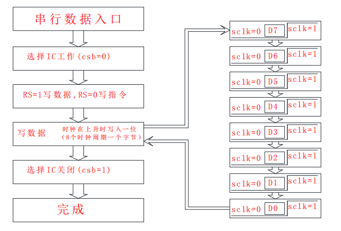
First, pull down CSB;
Select write data or instruction by setting the level of RS;
SCL is pulled down, bit7 is transmitted, SCL is pulled up, and so on. One byte is transmitted from bit7 to bit0;
Finally, pull up the CSB.
7. Write data flow
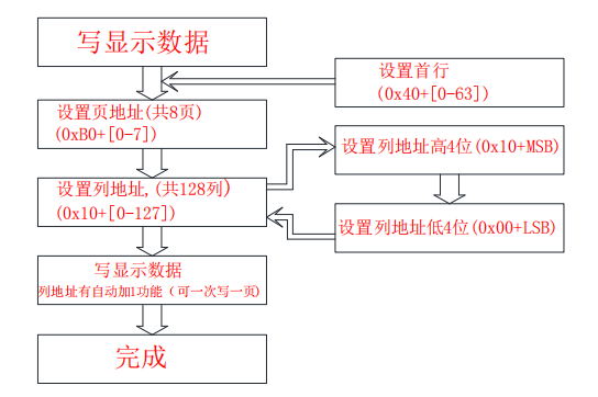
It can be seen that before writing data, the write address should be set first. Here are column address (0-127 columns) and page address (0-7 pages). At the same time, it should be noted that the column address will be added automatically.
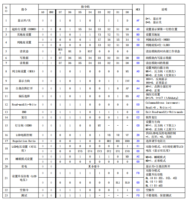
8. Instruction description
9. Principle design
10. Program driver
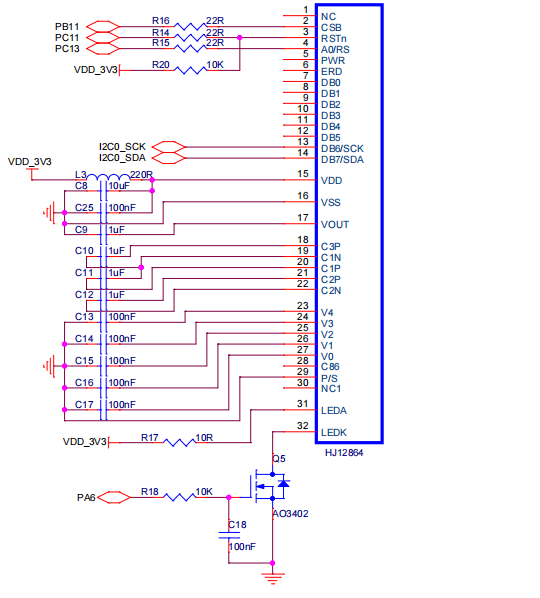
This paper uses GD32 to drive LCD.
10.1 definition and initialization of io port
#define LCD_SCL_PORT         GPIOB
#define LCD_SCL_PIN          GPIO_PIN_6

#define LCD_SDA_PORT         GPIOB
#define LCD_SDA_PIN          GPIO_PIN_7

#define LCD_CSB_PORT         GPIOB
#define LCD_CSB_PIN          GPIO_PIN_11

#define LCD_RST_PORT         GPIOC
#define LCD_RST_PIN          GPIO_PIN_11

#define LCD_A0_PORT          GPIOC
#define LCD_A0_PIN           GPIO_PIN_13

#define LCD_BKLED_PORT       GPIOA
#define LCD_BKLED_PIN        GPIO_PIN_6

#define LCD_CMD  		     1
#define LCD_DATA             0

#define PORT(port)       	 LCD_##port##_PORT
#define PIN(pin)         	 LCD_##pin##_PIN

#define LCD_PIN_OUT(pin,level) { if(level)                               \
							     { gpio_bit_set(PORT(pin),PIN(pin));}    \
							     else                                    \
							     { gpio_bit_reset(PORT(pin),PIN(pin));}  \
                               }
void LcdIoInit(void)
{
	rcu_periph_clock_enable(RCU_GPIOA);
	rcu_periph_clock_enable(RCU_GPIOB);
	rcu_periph_clock_enable(RCU_GPIOC);

	gpio_init(LCD_SCL_PORT, GPIO_MODE_OUT_PP, GPIO_OSPEED_50MHZ,  LCD_SCL_PIN);
	gpio_init(LCD_SDA_PORT, GPIO_MODE_OUT_PP, GPIO_OSPEED_50MHZ,  LCD_SDA_PIN);

	gpio_init(LCD_CSB_PORT, GPIO_MODE_OUT_PP, GPIO_OSPEED_50MHZ,  LCD_CSB_PIN);
	gpio_init(LCD_RST_PORT, GPIO_MODE_OUT_PP, GPIO_OSPEED_50MHZ,  LCD_RST_PIN);
	gpio_init(LCD_A0_PORT, GPIO_MODE_OUT_PP, GPIO_OSPEED_50MHZ,  LCD_A0_PIN);

	gpio_init(LCD_BKLED_PORT, GPIO_MODE_OUT_PP, GPIO_OSPEED_50MHZ,  LCD_BKLED_PIN);

	LCD_PIN_OUT(BKLED,1);
}
10.2 LCD write
/*
ismcd:High indicates data and low indicates instruction
*/
static void LcdWrite(uint8_t iscmd ,uint8_t data)
{
	uint8_t  i;

	LCD_PIN_OUT(CSB,0);
	if(iscmd)
	{
		LCD_PIN_OUT(A0,0);
	}
	else
	{
		LCD_PIN_OUT(A0,1);
	}
	for(i=0;i<8;i++)
	{
		LCD_PIN_OUT(SCL,0);
		 DelayUs(10);
		if(data&0x80)
		{
			LCD_PIN_OUT(SDA,1);
		}
		else
		{
			LCD_PIN_OUT(SDA,0);
		}
		LCD_PIN_OUT(SCL,1);
		DelayUs(10);
		data=data<<1;
	}

	LCD_PIN_OUT(CSB,1);
}
10.3 LCD setting address
void LcdAddress(uint8_t  page,uint8_t column)
{
	LcdWrite(LCD_CMD,0xb0+page);
	LcdWrite(LCD_CMD,((column>>4)&0x0f)+0x10); //Set the upper 4 bits of the column address
	LcdWrite(LCD_CMD,((column>>0)&0x0f)+0x00); //Set the lower 4 bits of the column address
}
10.4 LCD clear screen
Screen clearing is to write 0 to the video memory, that is, it is not displayed.
/*Full screen clearing*/
void LcdClearScreen(void)
{
	uint8_t  i,j;

	for(i=0;i<8;i++)
	{
		LcdAddress(i,0);
		for(j=0;j<128;j++)
		{
			LcdWrite(LCD_DATA,0x00);
		}
	}
}
10.5 LCD display frame
void LcdDispBK(void)
{
	uint8_t  i;

	//Upper frame
	LcdAddress(0,0);
	for (i=0;i<128;i++)
	{
		LcdWrite(LCD_DATA,0x01);
	}
	//Lower frame
	LcdAddress(7,0);
	for (i=0;i<128;i++)
	{
		LcdWrite(LCD_DATA,0x80);
	}

	//Left frame
	for(i=0;i<8;i++)
	{
		LcdAddress(i,0);
		LcdWrite(LCD_DATA,0xff);
	}
	//Right frame
	for(i=0;i<8;i++)
	{
		LcdAddress(i,127);
		LcdWrite(LCD_DATA,0xff);
	}
}
10.6 LCD displays 8 * 16 string
void LcdDispStr8x16(uint8_t reverse,uint8_t page,uint8_t column,uint8_t *str)
{
	uint16_t i=0,j;
	uint8_t zk[16];

	while(str[i]>0x00)
	{
		if((str[i]>=0x20)&&(str[i]<=0x7e))
		{
			extern uint8_t  GT20L16S1YGetAsciiData( uint8_t ASCIICode, uint32_t BaseAdd, uint8_t* S1YDZ_Data );

			GT20L16S1YGetAsciiData( str[i], 0x3b7c0, zk);

			LcdAddress(page,column); //Upper half
			for(j=0;j<8;j++)
			{
				if (reverse==1)
				{
					LcdWrite(LCD_DATA,zk[j]);
				}
				else
				{
					LcdWrite(LCD_DATA,~(zk[j]));
				}
			}
			LcdAddress(page+1,column);//Lower half

			for(j=0;j<8;j++)
			{
				if (reverse==1)
				{
					LcdWrite(LCD_DATA,zk[j+8]);
				}
				else
				{
					LcdWrite(LCD_DATA,~(zk[j+8]));
				}
			}
			i++;
			column+=8;
		}
	}
}
Used in this article GT20L16S1Y Font, so lattice data is read directly from the font.
10.7 LCD display 16 * 16 Chinese characters
void LcdDispStr16x16(uint8_t reverse,uint8_t page,uint8_t column,uint8_t *str)
{
	uint16_t i=0,j;
	uint8_t zk[32];

	while(str[i]>0x00)
	{
		extern  void GT20L16S1YGetGb2312Data( uint8_t MSB, uint8_t LSB, uint8_t* S1YDZ_Data );

		GT20L16S1YGetGb2312Data( str[i], str[i+1], zk );

		LcdAddress(page,column); //Upper half
		for(j=0;j<16;j++)
		{
			if (reverse==1)
			{
				LcdWrite(LCD_DATA,zk[j]);
			}
			else
			{
				LcdWrite(LCD_DATA,~(zk[j]));
			}
		}
		LcdAddress(page+1,column);//Lower half

		for(j=0;j<16;j++)
		{
			if (reverse==1)
			{
				LcdWrite(LCD_DATA,zk[j+16]);
			}
			else
			{
				LcdWrite(LCD_DATA,~(zk[j+16]));
			}
		}
		i++,i++;
		column+=16;
	}
}
Used in this article GT20L16S1Y Font, so lattice data is read directly from the font.
10.8 LCD initialization
void LcdInit(void)
{
	LcdIoInit();

	LCD_PIN_OUT(RST,0);
	DelayUs(20);
	LCD_PIN_OUT(RST,1);     /*Reset complete*/
	DelayUs(20);
	LcdWrite(LCD_CMD,0xe2); /*Soft reset*/
	DelayUs(50);
	LcdWrite(LCD_CMD,0x2c); /*Boost step 1*/
	DelayUs(50);
	LcdWrite(LCD_CMD,0x2e); /*Boost step 2*/
	DelayUs(50);
	LcdWrite(LCD_CMD,0x2f); /*Boost step 3*/
	DelayUs(50);

	LcdWrite(LCD_CMD,0x24); /*Coarse contrast adjustment, settable range 0x20 ~ 0x27*/
	LcdWrite(LCD_CMD,0x81); /*Fine tune contrast*/

	LcdWrite(LCD_CMD,0x1b); /*0x1a,Fine tune the contrast value, and the range can be set from 0x00 to 0x3f 1f*/
	LcdWrite(LCD_CMD,0xa3); /*Bias ratio (bias), 0xa2:1 / 9 0xa3:1 = 1 / 7    */

	LcdWrite(LCD_CMD,0xc8); /*Line scanning order: top to bottom*/
	LcdWrite(LCD_CMD,0xa0); /*Column scan order: left to right*/
	LcdWrite(LCD_CMD,0x40); /*Start line: the first line starts*/

	LcdWrite(LCD_CMD,0xaf); /*On display*/
	LcdClearScreen();
	LcdDispBK();

	LcdDispStr8x16(0,2,20,(uint8_t*)"display,test") ;
	LcdDispStr16x16(1,5,50,(uint8_t*)"Hello");
}
Note: if the display is not clear, it can be adjusted by bias ratio and contrast.
11. Display test
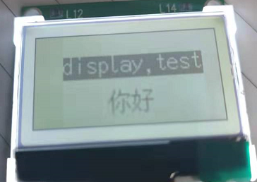
The figure shows Chinese, English and border, and also realizes anti display.