Used as a record of the learning process
1 Preparation
Software part
ise14.7 mainly completes the programming and pin binding of FPGA development board. modelsim simulates the spi communication process of verilog program to judge whether the program can be effectively executed. ADF435X is a simulation software for ADF4351 chip, which judges the theoretical value of output according to the input by setting the number of internal registers. AD software is the software used to draw PCB, and then place an order for PCB through jialichuang.
hardware component

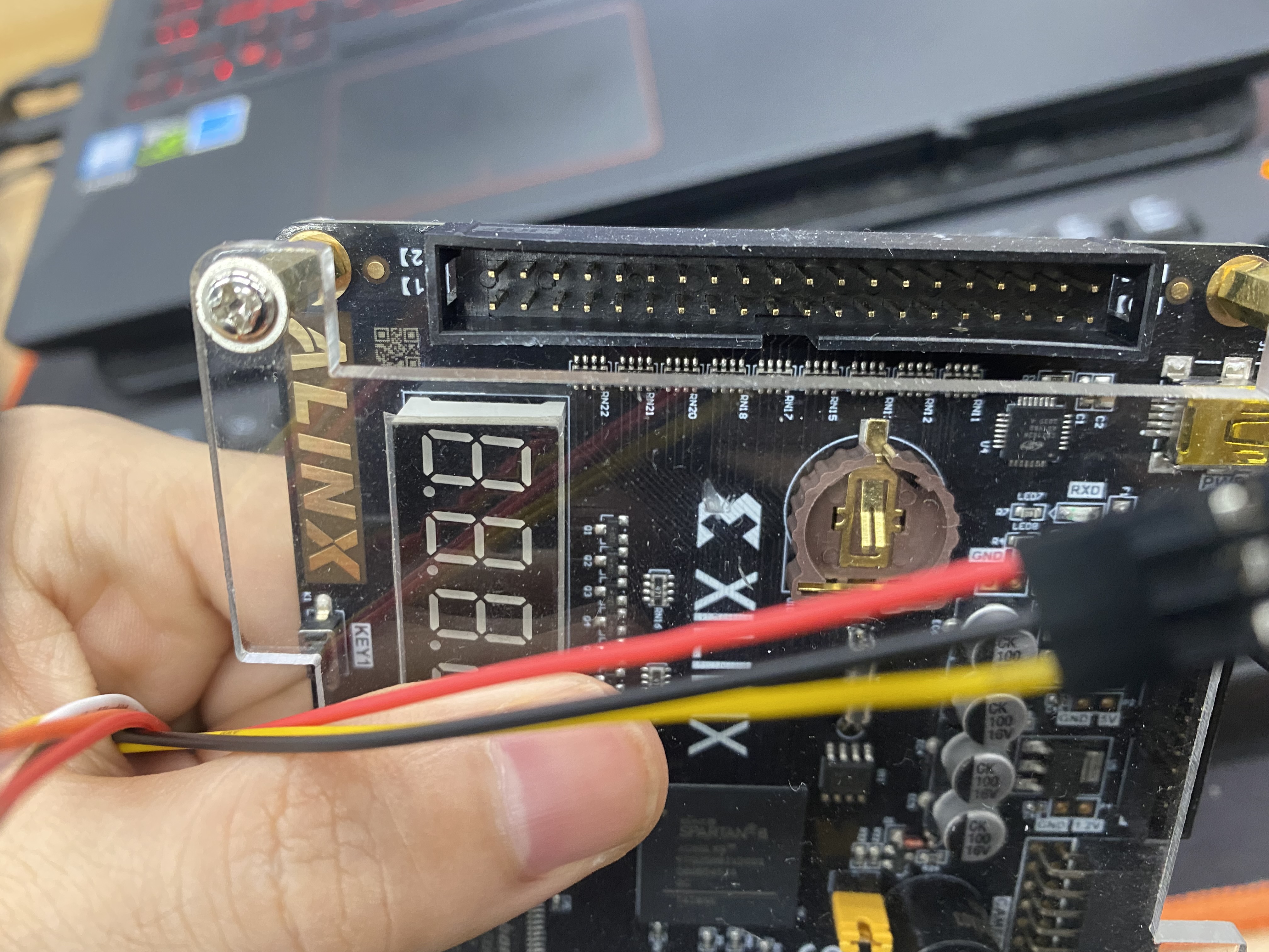
The hardware part is mainly a signal generator, oscilloscope or frequency meter, as well as a FPGA development board (I use alinx black gold development board, equipped with spartan-6) and ADF4351 chip (the chip performance is no longer introduced, and the manual of chip can be found on the Internet).
Main process
In fact, the process is mainly divided into two parts, one is the convenient programming of software, and the other is the pcb board making and welding of hardware.
ISE program written to development board
The establishment of ISE complete project will not be repeated. This article I refer to, Establishment of a complete ise project And alinx's teaching documents. This step is actually the most complex. Beginners like me spend a lot of time. For pin binding, please refer to the user manual of the development board and the demo file of the teaching file as a reference. Here I use modelsim for simulation.
The verilog program is as follows: the value written to the register has also been set,
`timescale 1ns / 1ps
//
module ADF4351#
   (
    parameter r0=32'h0fa00000,
    parameter r1=32'h00008011,
    parameter r2=32'h0c08dfc2,
    parameter r3=32'h004004b3,
    parameter r4=32'h00b040bc,
    parameter r5=32'h00580005
   )
   (
    input clk,
    input config_start,
    output reg config_end=1'b0,
    output reg sclk=1'b0,
    output reg csn=1'b1,
    output reg le=1'b0,
    output reg dout=1'b0
    );
///*edge_config_start*
reg [1:0] edge_config_check=2'b00;
wire edge_config_start;
assign edge_config_start=~edge_config_check[1] & edge_config_check[0];
always@(posedge clk) edge_config_check<={edge_config_check[0],config_start};
  vb///*trans_data*//
localparam addr_r0=3'b000,addr_r1=3'b001,addr_r2=3'b010,addr_r3=3'b011,addr_r4=3'b100,addr_r5=3'b101;
reg [2:0] addr_reg=3'b101;
reg delay=1'b0;
reg [31:0] trans_data=32'h00000000;
always@(*)
case(addr_reg)
addr_r0:trans_data<=r0;
addr_r1:trans_data<=r1;
addr_r2:trans_data<=r2;
addr_r3:trans_data<=r3;
addr_r4:trans_data<=r4;
addr_r5:trans_data<=r5;
default:;
endcase
///*dout*/
localparam start=1'b0,process=1'b1;
reg status=start;
reg [4:0] addr_bit=5'b00000;
always@(posedge clk)
case(status)
start:
if(edge_config_start)
  begin csn<=1'b0;
        dout<=r5[31];
        addr_bit<=5'b11111;
        addr_reg<=3'b101;
        config_end<=1'b0;
        status<=process;
  end
else if(~csn)
       if(~sclk && ~delay)
         sclk<=1'b1;
       else if(sclk)
              begin sclk<=1'b0;
                    dout<=r5[31];
                    addr_bit<=5'b11111;
                    addr_reg<=3'b101;
              end
       else if(~config_end)
              begin csn<=1'b1;
                    config_end<=1'b1;
              end
            else ;
     else ;
process:
if(~sclk && ~delay && ~le)
  sclk<=1'b1;
else if(~sclk && delay) ;
else if((addr_reg==3'b000) && (addr_bit==5'b00001))
       begin dout<=trans_data[addr_bit-1'b1];
             addr_bit<=addr_bit-1'b1;
             sclk<=1'b0;
             status<=start;
       end
else if(addr_bit==5'b00000)
       begin dout<=trans_data[31];
             addr_bit<=5'b11111;
             addr_reg<=addr_reg-1'b1;
             sclk<=1'b0;
       end
else begin dout<=trans_data[addr_bit-1'b1];
           addr_bit<=addr_bit-1'b1;
           sclk<=1'b0;
     end
default:;
endcase
///*delay*/
always@(posedge clk)
if((addr_bit==5'b00000) && ~sclk)
  delay<=1'b1;
else if(~(addr_bit==5'b00000) && ~sclk && le)
       delay<=1'b0;
     else ;
*le*
always@(posedge clk)
if(delay && ~sclk)
  le<=1'b1;
else if(le)
       le<=1'b0;
     else ;
endmodule
Setting stop time, clock signal and reset signal in the simulated text fixture file, and then calling modelsim to simulate, you can get the following picture.
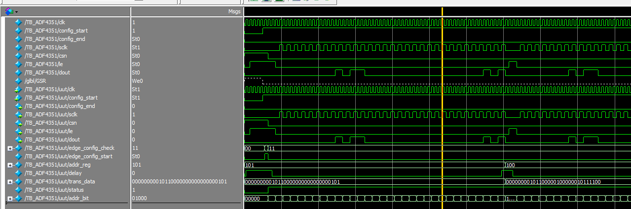
You can see that the data is written to the specified register in turn, and the spi communication is successfully established. It is consistent with the sequence diagram in ADF4351 manual.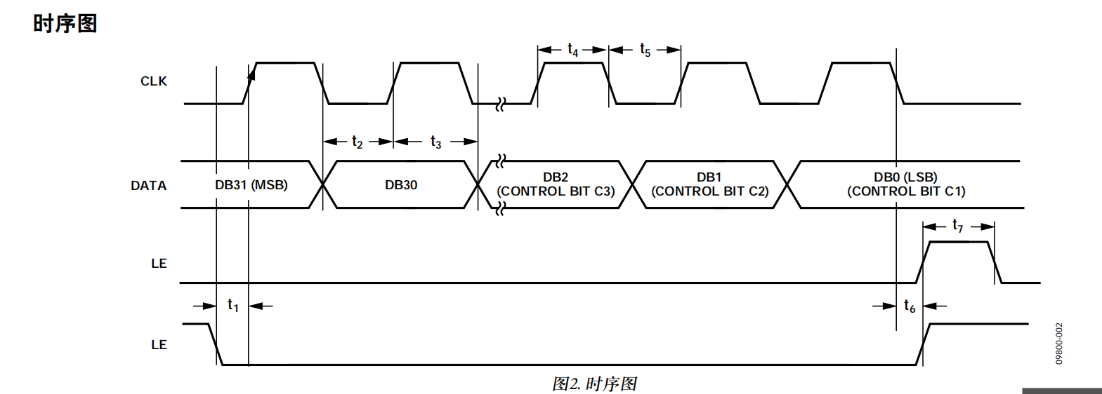
Then burn the verilog program into the development board. The development board program is ready.
Design and welding of PCB
Go directly to the finished product. In the design process, I mainly refer to this video, A flow explanation video of ad software , the effect of the PCB designed and welded by myself is not ideal, so I temporarily use the PCB welded by my senior brother. I'm lazy.
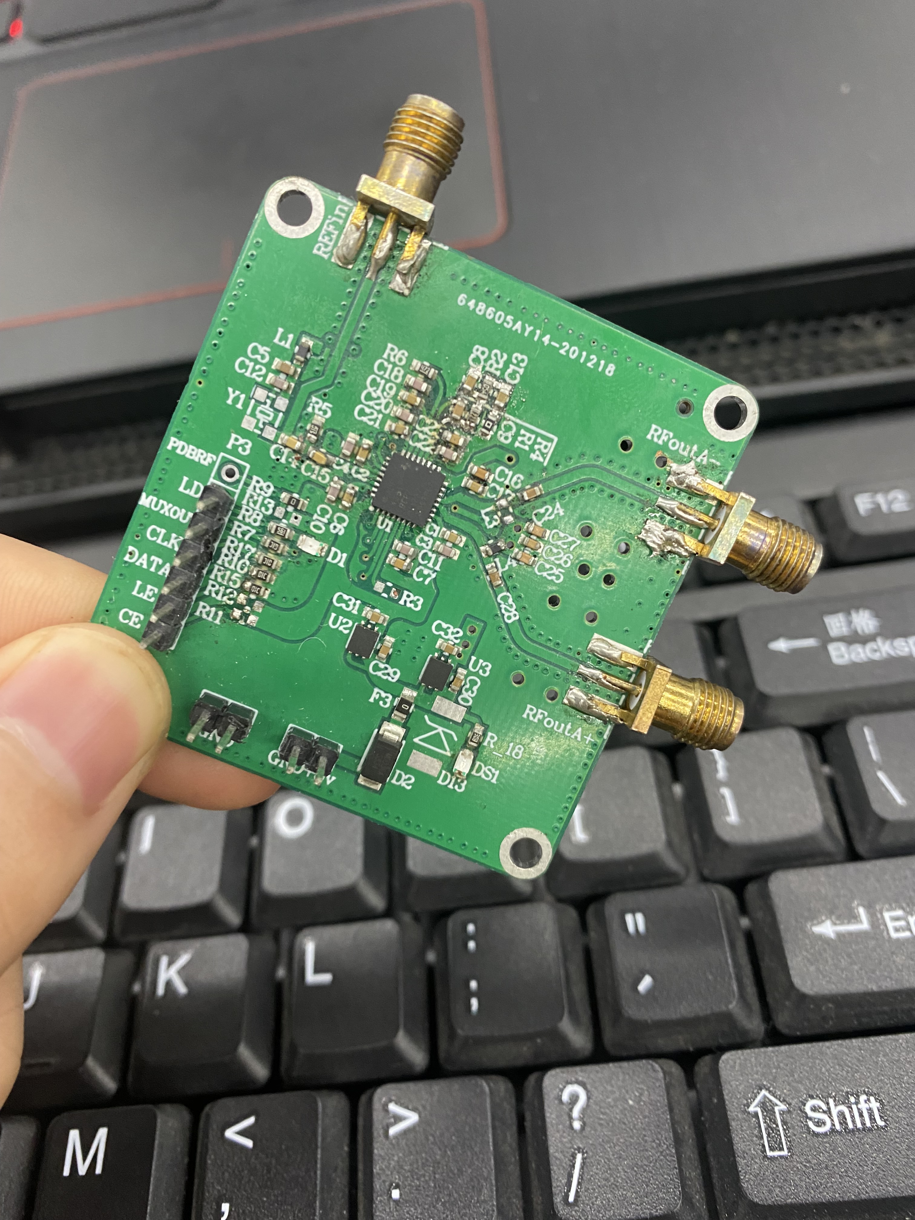
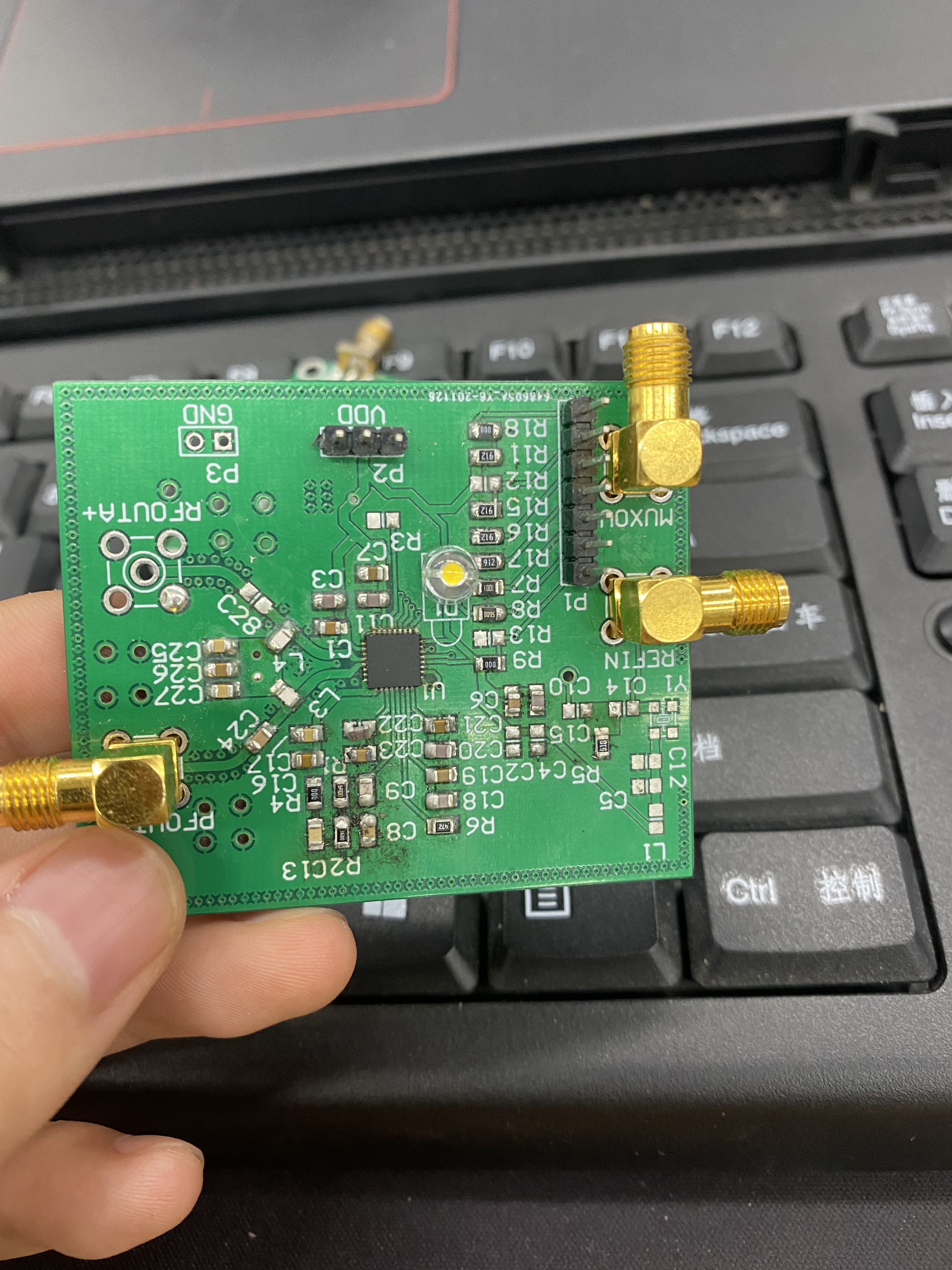
The effect of the two PCBs is the same, but the models of electronic components are different. Just use DuPont line to connect the PCB pin with the FPGA development board pin. Note that the voltage and ground should also be connected. According to the pin connection set in ise, the expansion port of black gold development board is as follows.
experimental result
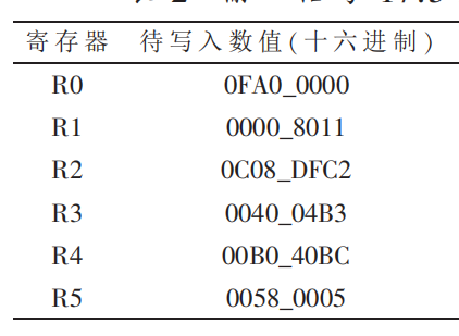
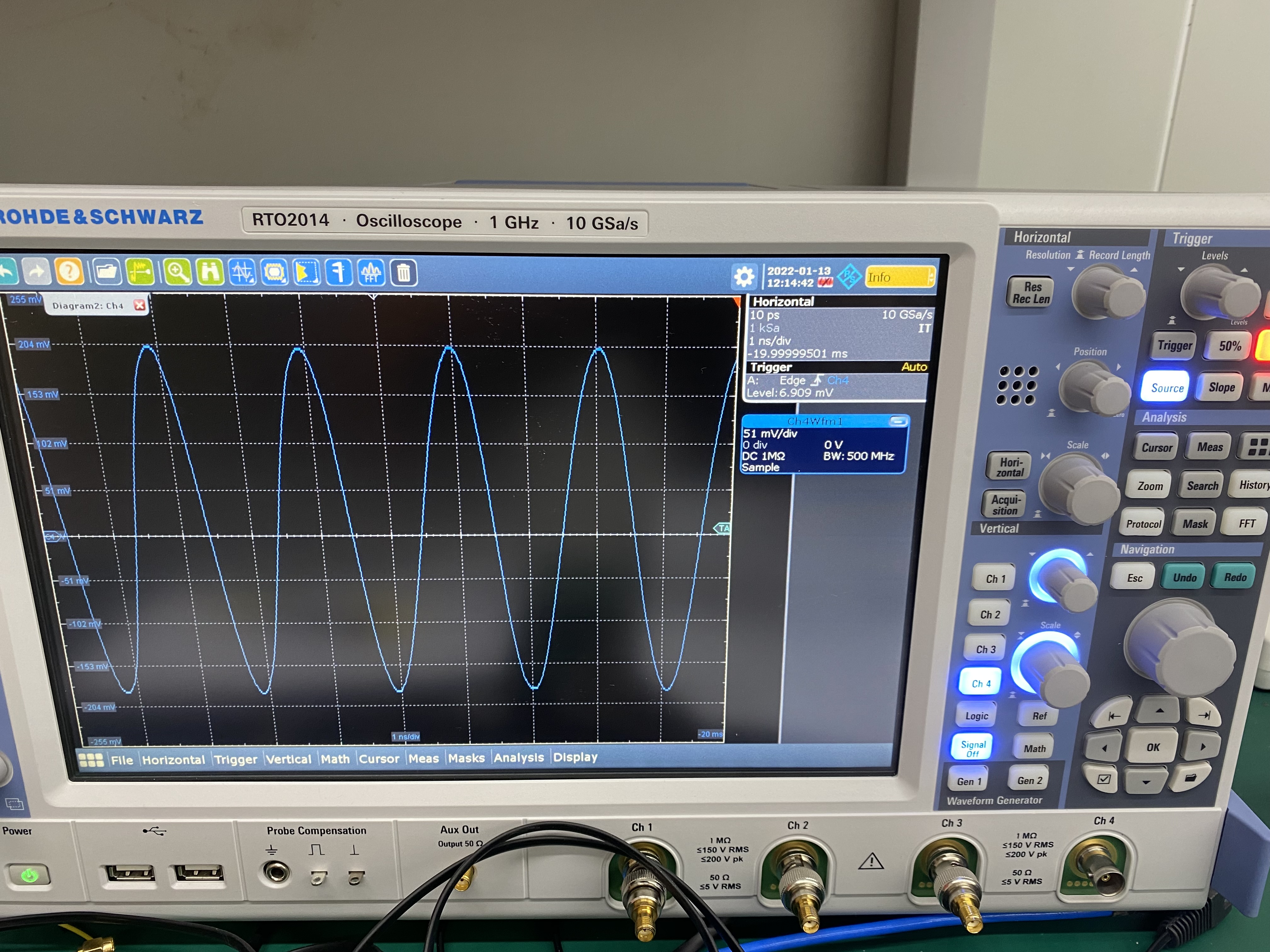
When setting the register in this way, it can be obtained through the simulation of the simulation software. If the input is 17.5mhz, the output of 500mhz can be obtained. The register value in the program is set in this way.
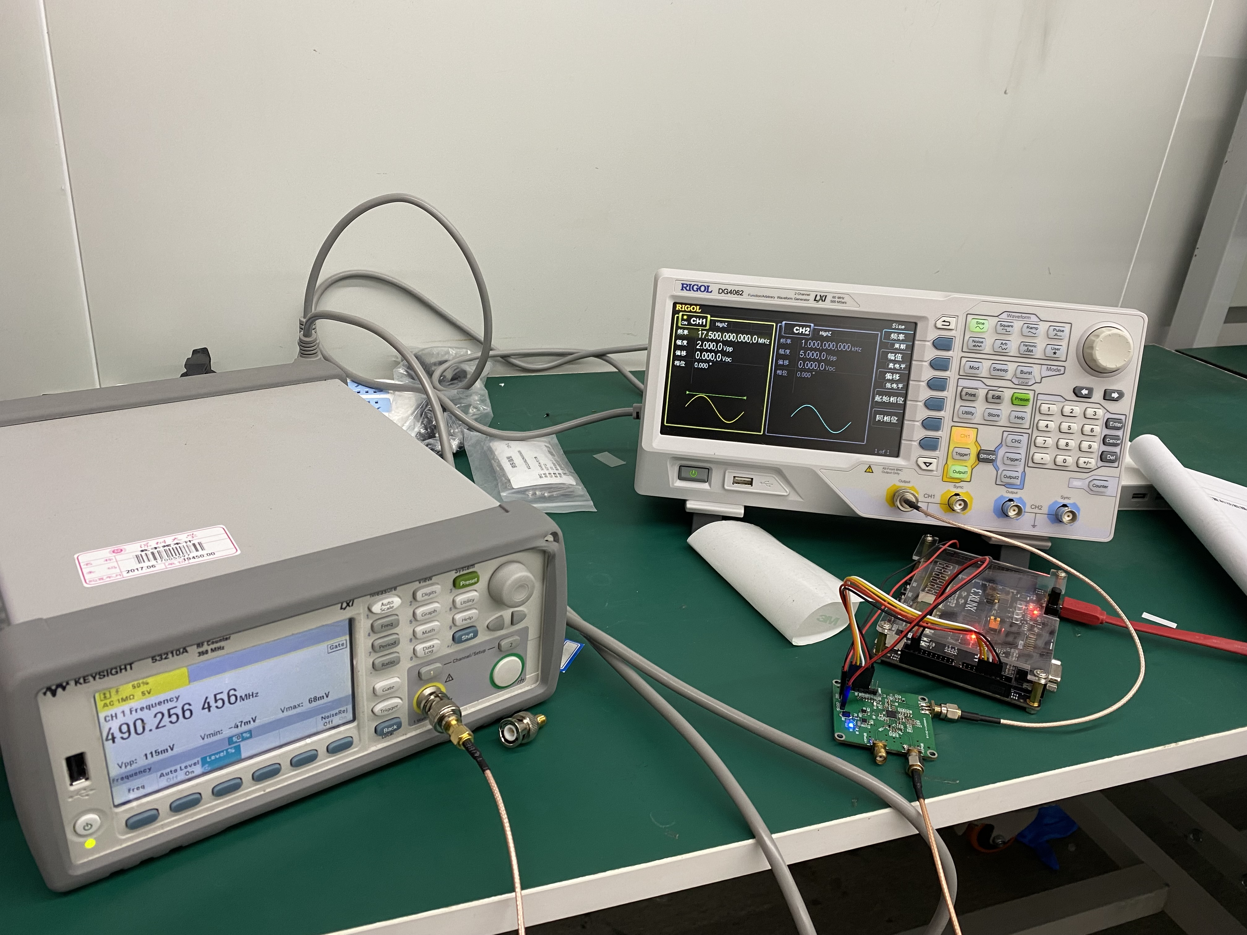
In the figure above, the signal generator generates a 17.5mhz sine wave with an output frequency of 490.256mhz. Although there is error, it preliminarily proves that the FPGA control of ADF4351 has been realized. Later, as long as the register value in the program is changed, and then written into the development board again, and the development board writes the value into the register of ADF chip, the control can be realized.
[1] Wang Han, Cheng Cheng, Shi Jiaru Design of synthetic frequency source based on ADF4351 and FPGA [J] Application of electronic technology, 2017,43 (10): 34-38 + 43 DOI:10.16157/j.issn. 0258-7998.171271.