Platform: Code Composer Studio 10.3.1
MSP430F5529 LaunchPad™ Development Kit
(MSP‑EXP430F5529LP)
Hard knowledge
Introduction to comparator B
The comparator B module contains the comparison function of up to 16 channels and has the following characteristics:
inverting and in-phase input multiplexers;
comparator output programmable RC filter;
output is provided to timer A capture input;
port input buffer program control;
interruption capability;
optional reference voltage generator and voltage lag generator;
external reference voltage input;
ultra low power comparator mode;
interrupt driven measurement system - supports low-power operation.
The structural block diagram of comparator B is shown in the figure.
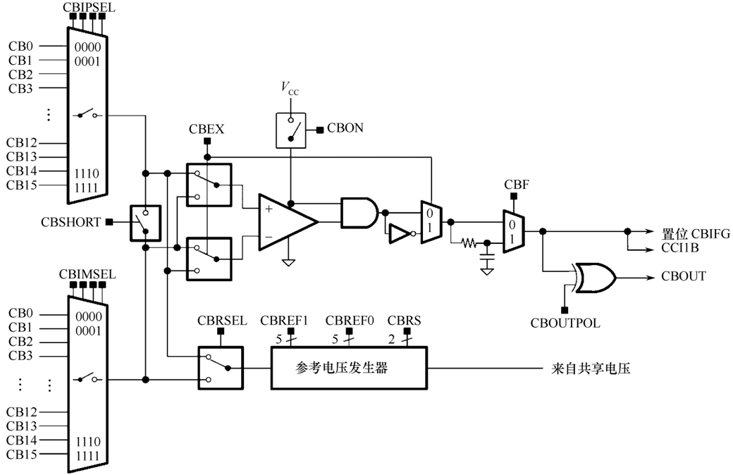
Analog input switch
The analog input switch controls the input of analog signal through CBIPSEL and SBIMSEL control bits. Each input channel is relatively independent and can be introduced into the "+" input or "-" input of comparator B. The analog signal input of comparator B can be short circuited through the CBSHORT control bit. The input of comparator B can also introduce the reference voltage generated by the internal reference voltage generator through the cooperation of CBRSEL and CBEX control bits.
Through the configuration of corresponding registers, comparator B can compare the following analog voltage signals:
comparison of two external input voltage signals;
comparison between each external input voltage signal and internal reference voltage.
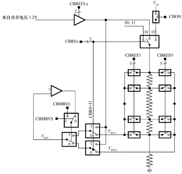
Reference voltage generator
The structural block diagram of the reference voltage generator of comparator B is shown in the figure.
The reference voltage generator generates different reference voltages VREF by connecting trapezoidal resistance circuit or internal shared voltage. As shown in the figure, the CBRSx control bit can select the source of the reference voltage. If CBRSx is 10, the internal ladder resistance circuit voltage comes from the internal shared voltage, which can generate 1.5V, 2.0V or 2.5V through the CBREFLx control bit. If CBRSx is 01, the voltage of internal ladder resistance circuit comes from VCC, and the switching of reference power supply can be realized through CBON. If CBRSx is 00 or 11, the internal ladder resistance circuit has no power available and is prohibited. If CBRSx is 11, the reference voltage comes from the internal shared voltage. When CBRSx is not 11, when CBMRVS is 0 and CBOUT is 1, the reference voltage comes from VREF1; When both CBMRVS and CBOUT are 0, the reference voltage comes from VREF0. When the ladder resistance circuit is available, the reference voltage source can be divided by CBREF1 and CBREF0 control bits, and the voltage division multiples can be 1 / 5, 2 / 5, 3 / 5, 4 / 5, 1 / 4, 3 / 4, 1 / 3, 2 / 3, 1 / 2 and 1. The CBMRVS control bit controls the source signal controlling the VREF voltage. If CBMRVS control bit is 0, CBOUT controls the source of VREF voltage signal; If the CBMRVS control bit is 1, the CBMRVL control bit controls the source of the VREF voltage signal.
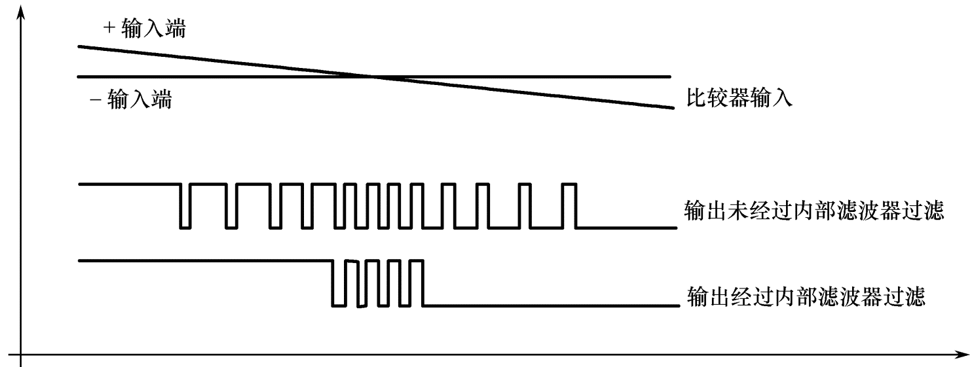
Internal filter
The output of comparator B can choose to use or not use an internal RC filter. When the CBF control bit is set to 1, the output signal of the comparator is RC filtered. On the contrary, RC filtering is not used.
If the voltage difference of the analog voltage is very small at the input of the comparator, the output of the comparator will oscillate. As shown in figure 6.3.3, when the voltage at the "+" input of the comparator decreases and crosses the reference comparison voltage at the "-" input, if the comparator output is not filtered by the internal filter, the comparator output will produce large oscillation at the time of voltage crossing; If the output of the comparator is filtered by an internal filter, the output oscillation of the comparator is small at the time of voltage crossing.
Comparator B measuring resistance principle
The circuit diagram of measuring resistance with comparator B is shown in the figure. The measured resistance and A standard reference resistance are respectively connected to two GPIO ports. The measured resistance can be fixed or variable, such as temperature control resistance. The other end of the measured resistance and the standard resistance is connected with A fixed capacitor and connected to the positive input of comparator B. The negative input terminal of the comparator is connected to the internal 0.25VCC reference voltage, and the comparator output is connected to timer A.
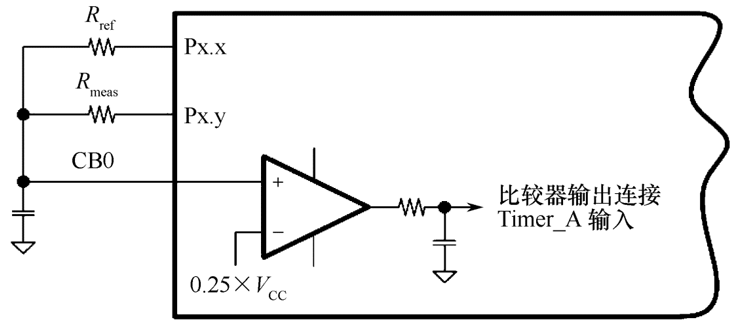
The measurement process of the measured resistance is as follows:
Set px The x pin is pulled up and the capacitor is charged through the standard reference resistance Rref;
Set px The x pin is pulled down and the capacitor is discharged through the standard reference resistance Rref;
Then px The x pin is pulled up and the capacitor is charged through the standard reference resistance Rref;
Then px Y pin is pulled down and the capacitor is discharged through the measured resistance Rmeas.
In this way, the timer A is used to accurately measure the time of discharging the capacitor through Rref and Rmeas. The measurement process is shown in the figure.
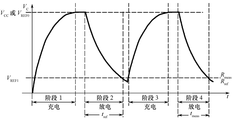
The calculation formula of the measured resistance is
Where Nmeas is the capture count value of timer A when the capacitor discharges through the measured resistance; Nref is the capture count value of timer A when the capacitor discharges through the standard reference resistance.
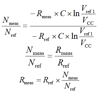
Principle of capacitive touch key using comparator B
The human body has a certain capacitance. When we draw the copper on the PCB as shown in the figure, we make a basic touch sensitive key.
The figure on the left in the figure above shows a basic touch button. The central circular shadow part is copper (which can be called "key"), in which a wire will be led out to connect with the single chip microcomputer. The single chip microcomputer will detect whether there is a key "pressed" through this wire (the detection method will be introduced later); The shaded part of the periphery is also copper, but these copper in the periphery are connected to GND earth. There is a gap between the "key" and the peripheral copper (which can be called gap d). The right figure in figure 6.3.6 is the cross-sectional view of the left figure. When there is no finger contact, there is only one capacitance Cp; When a finger contacts, the "key" forms a capacitance Cf through the finger. Since the two capacitors are connected in parallel, the change rate of the total capacitance before and after the finger contacts the "key" is C% = ((Cp+Cf)- Cp)/ Cp =Cf/Cp.
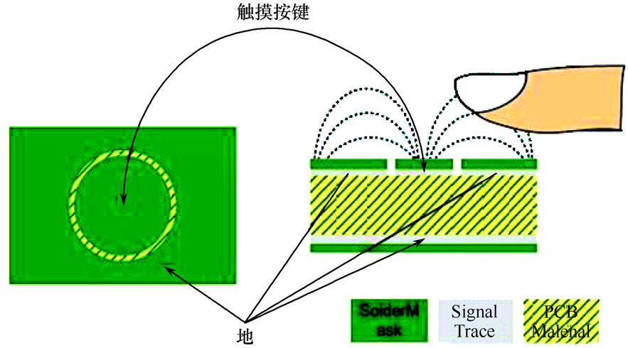
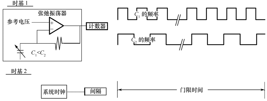
The circuit of using comparator B to realize A relaxation oscillation touch key is shown in figure 6.3.8. At the input terminal, the positive input terminal of the comparator is connected with the internal reference voltage, the negative input terminal of the comparator is connected between the resistance Rc and the induction capacitor, and CBOUT is connected with TACLK. When there is no voltage at both ends of the induction capacitor CSENSOR, CBOUT will output A high level through the comparison of comparator B, and then charge the induction capacitor through Rc. When the voltage at both ends of the induction capacitor is higher than the reference voltage at the "+" input of the internal comparator, CBOUT will output A low level through the comparison of comparator B, and the induction capacitor will discharge through Rc. In the process of discharge, if the voltage at both ends of the induction capacitor is lower than the reference voltage at the "+" input of the internal comparator, CBOUT outputs A high level. Discharge the induction capacitor through Rc. In this way, the output CBOUT of comparator B will output A rectangular wave with A certain frequency. The frequency of the rectangular wave can reflect the charge and discharge time of the induction capacitor, and then the change of the induction capacitor can be detected. Therefore, it is only necessary to use timer A as A frequency meter to calculate the output frequency of the relaxation oscillator within A fixed time. If the output frequency changes greatly at A certain time, it means that the capacitance value has been changed, that is, the key has been "pressed".
The schematic diagram of the capacitance touch key detection method based on the relaxation oscillator is shown in the figure below. When the finger touches the capacitance touch key, the capacitance changes from C1 to C2, and the output frequency of the relaxation oscillator will be greatly reduced. Then, use the timer to calculate the output frequency of comparator B within the threshold time to detect the induced capacitance.
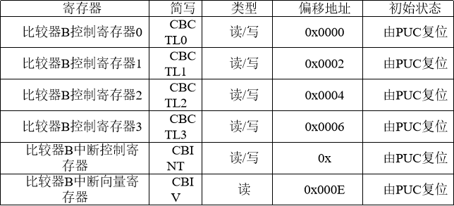
Comparator B control register
COMP_ API B (mechanical turnover)
introduce
COMP_ The B API provides a set of comps using msp430ware_ Function of module B. Initialization comp is provided_ B module, setting input reference voltage and managing comp_ Function interrupted by module B.
COMP_ Module B provides the ability to compare two analog signals and uses available software and output pins to indicate whether the positive end signal is higher than the negative end signal. COMP_B can be used to produce hysteresis. You can use 16 different inputs or as few as 2 inputs. COMP_ The B module can also control the REF module to generate a reference voltage as an input.
COMP_ Module B can generate multiple interrupts. An interrupt can be generated for the output, or the output is divided into rising or falling separate interrupts.
COMP_ The B API is divided into three groups of functions:
Functions that handle initialization and output,
Functions that handle interrupts,
Processing COMP_B function of auxiliary characteristics.
Functions that handle initialization and output
Comp_B_init(uint16_t baseAddress, Comp_B_initParam ∗ param)
//Initialize Comp B module
Comp_B_configureReferenceVoltage(uint16_t baseAddress, Comp_B_configureReferenceVoltageParam ∗ param)
//A reference voltage is generated to the selected terminal during initialization
Comp_B_selectReferenceVoltage(uint16_t baseAddress, uint16_t selectType, uint16_t selectVRef)
//Modify how the comparator output is selected between VREFO or VREF1
Comp_B_enable(uint16_t baseAddress)
//Open comp_ Module B
Comp_B_disable(uint16_t baseAddress)
//Close comp_ Module B
Comp_B_outputValue(uint16_t baseAddress)
//Returns the output value of Comp B module
parameter
baseAddress
COMP_B_BASE
Comp_B_initParam
//*****************************************************************************
//
//! \brief Used in the Comp_B_init() function as the param parameter.
//
//*****************************************************************************
typedef struct Comp_B_initParam {
    //! Selects the input to the positive terminal.
    //! \n Valid values are:
    //! - \b COMP_B_INPUT0 [Default]
    //! - \b COMP_B_INPUT1
    //! - \b COMP_B_INPUT2
    //! - \b COMP_B_INPUT3
    //! - \b COMP_B_INPUT4
    //! - \b COMP_B_INPUT5
    //! - \b COMP_B_INPUT6
    //! - \b COMP_B_INPUT7
    //! - \b COMP_B_INPUT8
    //! - \b COMP_B_INPUT9
    //! - \b COMP_B_INPUT10
    //! - \b COMP_B_INPUT11
    //! - \b COMP_B_INPUT12
    //! - \b COMP_B_INPUT13
    //! - \b COMP_B_INPUT14
    //! - \b COMP_B_INPUT15
    //! - \b COMP_B_VREF
    uint8_t positiveTerminalInput;
    //! Selects the input to the negative terminal.
    //! \n Valid values are:
    //! - \b COMP_B_INPUT0 [Default]
    //! - \b COMP_B_INPUT1
    //! - \b COMP_B_INPUT2
    //! - \b COMP_B_INPUT3
    //! - \b COMP_B_INPUT4
    //! - \b COMP_B_INPUT5
    //! - \b COMP_B_INPUT6
    //! - \b COMP_B_INPUT7
    //! - \b COMP_B_INPUT8
    //! - \b COMP_B_INPUT9
    //! - \b COMP_B_INPUT10
    //! - \b COMP_B_INPUT11
    //! - \b COMP_B_INPUT12
    //! - \b COMP_B_INPUT13
    //! - \b COMP_B_INPUT14
    //! - \b COMP_B_INPUT15
    //! - \b COMP_B_VREF
    uint8_t negativeTerminalInput;
    //! Selects the power mode at which the Comp_B module will operate at.
    //! \n Valid values are:
    //! - \b COMP_B_POWERMODE_HIGHSPEED [Default]
    //! - \b COMP_B_POWERMODE_NORMALMODE
    //! - \b COMP_B_POWERMODE_ULTRALOWPOWER
    uint16_t powerModeSelect;
    //! Controls the output filter delay state, which is either off or enabled
    //! with a specified delay level. This parameter is device specific and
    //! delay levels should be found in the device's datasheet.
    //! \n Valid values are:
    //! - \b COMP_B_FILTEROUTPUT_OFF [Default]
    //! - \b COMP_B_FILTEROUTPUT_DLYLVL1
    //! - \b COMP_B_FILTEROUTPUT_DLYLVL2
    //! - \b COMP_B_FILTEROUTPUT_DLYLVL3
    //! - \b COMP_B_FILTEROUTPUT_DLYLVL4
    uint8_t outputFilterEnableAndDelayLevel;
    //! Controls if the output will be inverted or not
    //! \n Valid values are:
    //! - \b COMP_B_NORMALOUTPUTPOLARITY [Default]
    //! - \b COMP_B_INVERTEDOUTPUTPOLARITY
    uint16_t invertedOutputPolarity;
} Comp_B_initParam;
Comp_B_configureReferenceVoltageParam
//*****************************************************************************
//
//! \brief Used in the Comp_B_configureReferenceVoltage() function as the param
//! parameter.
//
//*****************************************************************************
typedef struct Comp_B_configureReferenceVoltageParam {
    //! Decides the source and max amount of Voltage that can be used as a
    //! reference.
    //! \n Valid values are:
    //! - \b COMP_B_VREFBASE_VCC
    //! - \b COMP_B_VREFBASE1_5V
    //! - \b COMP_B_VREFBASE2_0V
    //! - \b COMP_B_VREFBASE2_5V
    uint16_t supplyVoltageReferenceBase;
    //! Is the numerator of the equation to generate the reference voltage for
    //! the lower limit reference voltage.
    uint16_t lowerLimitSupplyVoltageFractionOf32;
    //! Is the numerator of the equation to generate the reference voltage for
    //! the upper limit reference voltage.
    uint16_t upperLimitSupplyVoltageFractionOf32;
    //!  is the reference accuracy setting of the Comp_B. Clocked is for low
    //! power/low accuracy.
    //! \n Valid values are:
    //! - \b COMP_B_ACCURACY_STATIC
    //! - \b COMP_B_ACCURACY_CLOCKED
    uint16_t referenceAccuracy;
} Comp_B_configureReferenceVoltageParam;
selectType
/*determines whether VREF instance is chosen automatically or manually Valid
values are:*/
COMP_B_VREF_AUTO_SELECT /* [Default] - VREF instance is chosen by comparator output state.*/
COMP_B_VREF_MANUAL_SELECT /*- VREF instance is chosen by user (CBCTL1. CBMRVL bit)
Modified bits are CBMRVS of CBCTL1 register.*/
selectVRef
/*selects VREF0 or VREF1. Only applicable if VREF instance is set up to be
chosen manually Valid values are:*/
COMP_B_SELECT_VREF0 /*[Default]*/
COMP_B_SELECT_VREF1
/*Modified bits are CBMRVL of CBCTL1 register*/
Functions that handle interrupts
Comp_B_enableInterrupt(uint16_t baseAddress, uint16_t interruptMask)
//Enable the selected Comp B interrupt source
Comp_B_disableInterrupt(uint16_t baseAddress, uint16_t interruptMask)
//Disable the selected Comp B interrupt source
Comp_B_clearInterrupt(uint16_t baseAddress, uint16_t interruptFlagMask)
//Clear Comp_B interrupt flag
Comp_B_getInterruptStatus(uint16_t baseAddress, uint16_t interruptFlagMask)
//Get the current Comp B interrupt status
Comp_B_setInterruptEdgeDirection(uint16_t baseAddress, uint16_t edgeDirection)
//Sets the edge direction that will trigger the interrupt
Comp_B_toggleInterruptEdgeDirection(uint16_t baseAddress)
//Reverse the direction of the edge that will trigger the interrupt
parameter
baseAddress
COMP_B_BASE
interruptMask
/*is the bit mask of the interrupt sources to be enabled. Mask value is the logical
OR of any of the following:*/
COMP_B_OUTPUT_INT /*- Output interrupt*/
COMP_B_OUTPUTINVERTED_INT /*- Output interrupt inverted polarity*/
/*Modified bits of CBINT register.*/
interruptFlagMask
/*is a bit mask of the interrupt sources to be cleared. Mask value is the
logical OR of any of the following:*/
COMP_B_OUTPUT_FLAG /*- Output interrupt*/
COMP_B_OUTPUTINVERTED_FLAG /*- Output interrupt inverted
polarity
Modified bits of CBINT register.*/
edgeDirection
/*determines which direction the edge would have to go to generate an interrupt
based on the non-inverted interrupt flag. Valid values are:*/
COMP_B_RISINGEDGE /*[Default] - sets the bit to generate an interrupt
when the output of the Comp_B falls from LOW to HIGH if the normal
interrupt bit is set(and HIGH to LOW if the inverted interrupt enable bit is
set).*/
COMP_B_FALLINGEDGE /*- sets the bit to generate an interrupt when
the output of the Comp_B rises from HIGH to LOW if the normal interrupt
bit is set(and LOW to HIGH if the inverted interrupt enable bit is set).
Modified bits are CBIES of CBCTL1 register.*/
Processing COMP_B function of auxiliary characteristics
Comp_B_shortInputs(uint16_t baseAddress)
//Short circuit the two input pins selected during initialization
Comp_B_unshortInputs(uint16_t baseAddress)
//Disable the short circuit of the two input pins selected during initialization
Comp_B_disableInputBuffer(uint16_t baseAddress, uint8_t inputPort)
//Disables the input buffer of the selected input port to effectively allow analog signaling
Comp_B_enableInputBuffer(uint16_t baseAddress, uint8_t inputPort)
//Enables the input buffer of the selected input port to allow the passage of digital signals
Comp_B_swapIO(uint16_t baseAddress)
//Switch the bits of the input terminal and reverse comp at the same time_ B output
parameter
baseAddress
COMP_B_BASE
inputPort
//is the port in which the input buffer will be disabled. Valid values are:
COMP_B_INPUT0 //[Default]
COMP_B_INPUT1
COMP_B_INPUT2
COMP_B_INPUT3
COMP_B_INPUT4
COMP_B_INPUT5
COMP_B_INPUT6
COMP_B_INPUT7
COMP_B_INPUT8
COMP_B_INPUT9
COMP_B_INPUT10
COMP_B_INPUT11
COMP_B_INPUT12
COMP_B_INPUT13
COMP_B_INPUT14
COMP_B_INPUT15
COMP_B_VREF
//Modified bits are CBPDx of CBCTL3 register.
Actual combat
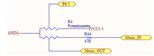
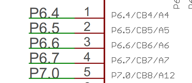
P6.5 (CB5) is the input, which is compared with the internally generated reference voltage
In normal mode, the filter selects the one with the shortest delay
    //Initialize the Comparator B module
    /*
     * Base Address of Comparator B,
     * Pin CB5 to Positive(+) Terminal
     * Reference Voltage to Negative(-) Terminal
     * Normal Power Mode
     * Output Filter On with minimal delay
     * Non-Inverted Output Polarity
     */
    Comp_B_initParam initParam = {0};
    initParam.positiveTerminalInput = COMP_B_INPUT5;
    initParam.negativeTerminalInput = COMP_B_VREF;
    initParam.powerModeSelect = COMP_B_POWERMODE_NORMALMODE;
    initParam.outputFilterEnableAndDelayLevel = COMP_B_FILTEROUTPUT_DLYLVL1;
    initParam.invertedOutputPolarity = COMP_B_NORMALOUTPUTPOLARITY;
    Comp_B_init(COMP_B_BASE, &initParam);
Set the lower threshold as Vcc*(11/32) = 1.134375V and the upper threshold as Vcc*(21/32) = 2.165625V
Static mode
    //Set the reference voltage that is being supplied to the (-) terminal
    /*
     * Base Address of Comparator B,
     * Reference Voltage = Vcc = 3.3V,
     * Lower Limit of Vcc*(11/32) = 1.134375V,
     * Upper Limit of Vcc*(21/32) = 2.165625V,
     * Static Mode Accuracy
     */
    Comp_B_configureReferenceVoltageParam refVoltageParam = {0};
    refVoltageParam.supplyVoltageReferenceBase = COMP_B_VREFBASE_VCC;
    refVoltageParam.lowerLimitSupplyVoltageFractionOf32 = 11;
    refVoltageParam.upperLimitSupplyVoltageFractionOf32 = 21;
    refVoltageParam.referenceAccuracy = COMP_B_ACCURACY_STATIC;
    Comp_B_configureReferenceVoltage(COMP_B_BASE, &refVoltageParam);
Enable the comparator and multiplex P1 6 is the comparator output
    //Allow power to Comparator module
    Comp_B_enable(COMP_B_BASE);

    GPIO_setAsPeripheralModuleFunctionOutputPin(GPIO_PORT_P1,GPIO_PIN6);
Overall code
#include "driverlib.h"

#define MCLK_IN_HZ      25000000

#define delay_us(x)     __delay_cycles((MCLK_IN_HZ/1000000*(x)))
#define delay_ms(x)     __delay_cycles((MCLK_IN_HZ/1000*(x)))

void SystemClock_Init(void)
{
    PMM_setVCore(PMM_CORE_LEVEL_3);     //High dominant frequency operation requires high core voltage

    //XT1 pin multiplexing
    GPIO_setAsPeripheralModuleFunctionInputPin(GPIO_PORT_P5, GPIO_PIN4);
    GPIO_setAsPeripheralModuleFunctionOutputPin(GPIO_PORT_P5, GPIO_PIN5);

    //Starting vibration XT1
    UCS_turnOnLFXT1(UCS_XT1_DRIVE_3,UCS_XCAP_3);

    //XT2 pin multiplexing
    GPIO_setAsPeripheralModuleFunctionInputPin(GPIO_PORT_P5, GPIO_PIN2);
    GPIO_setAsPeripheralModuleFunctionOutputPin(GPIO_PORT_P5, GPIO_PIN3);

    //Starting vibration XT2
    UCS_turnOnXT2(UCS_XT2_DRIVE_4MHZ_8MHZ);

    //XT2 is used as FLL reference clock, first 8 frequency division, then 50 frequency multiplication 4MHz / 8 * 50 = 25MHz
    UCS_initClockSignal(UCS_FLLREF, UCS_XT2CLK_SELECT, UCS_CLOCK_DIVIDER_8);
    UCS_initFLLSettle(25000, 50);

    //XT1 as ACLK clock source = 32768Hz
    UCS_initClockSignal(UCS_ACLK, UCS_XT1CLK_SELECT, UCS_CLOCK_DIVIDER_1);

    //DCOCLK as MCLK clock source = 25MHz
    UCS_initClockSignal(UCS_MCLK, UCS_DCOCLK_SELECT, UCS_CLOCK_DIVIDER_1);

    //DCOCLK as SMCLK clock source = 25MHz
    UCS_initClockSignal(UCS_SMCLK, UCS_DCOCLK_SELECT, UCS_CLOCK_DIVIDER_1);

    //Set the frequency of the external clock source so that when calling UCS_getMCLK, UCS_getSMCLK or UCS_ The correct value can be obtained when getaclk
    UCS_setExternalClockSource(32768, 4000000);
}

int main(void)
{
    WDT_A_hold(WDT_A_BASE);
    SystemClock_Init();

    //Initialize the Comparator B module
    /*
     * Base Address of Comparator B,
     * Pin CB5 to Positive(+) Terminal
     * Reference Voltage to Negative(-) Terminal
     * Normal Power Mode
     * Output Filter On with minimal delay
     * Non-Inverted Output Polarity
     */
    Comp_B_initParam initParam = {0};
    initParam.positiveTerminalInput = COMP_B_INPUT5;
    initParam.negativeTerminalInput = COMP_B_VREF;
    initParam.powerModeSelect = COMP_B_POWERMODE_NORMALMODE;
    initParam.outputFilterEnableAndDelayLevel = COMP_B_FILTEROUTPUT_DLYLVL1;
    initParam.invertedOutputPolarity = COMP_B_NORMALOUTPUTPOLARITY;
    Comp_B_init(COMP_B_BASE, &initParam);

    //Set the reference voltage that is being supplied to the (-) terminal
    /*
     * Base Address of Comparator B,
     * Reference Voltage = Vcc = 3.3V,
     * Lower Limit of Vcc*(11/32) = 1.134375V,
     * Upper Limit of Vcc*(21/32) = 2.165625V,
     * Static Mode Accuracy
     */
    Comp_B_configureReferenceVoltageParam refVoltageParam = {0};
    refVoltageParam.supplyVoltageReferenceBase = COMP_B_VREFBASE_VCC;
    refVoltageParam.lowerLimitSupplyVoltageFractionOf32 = 11;
    refVoltageParam.upperLimitSupplyVoltageFractionOf32 = 21;
    refVoltageParam.referenceAccuracy = COMP_B_ACCURACY_STATIC;
    Comp_B_configureReferenceVoltage(COMP_B_BASE, &refVoltageParam);

    //Allow power to Comparator module
    Comp_B_enable(COMP_B_BASE);

    GPIO_setAsPeripheralModuleFunctionOutputPin(GPIO_PORT_P1,GPIO_PIN6);

    __bis_SR_register(GIE);

    while(1)
    {

    }
}
Experimental phenomenon
Measure P1 with a multimeter 6 output voltage, it can be observed that when the CB5 input voltage is higher than the upper threshold voltage, P1 6 output 3.3V. When CB5 input voltage is lower than the lower threshold voltage, P1 6 output 0V. When it is between the two, the voltage changes continuously.