The development board has two timers: timer A and timer B. Since timer B is similar to timer A, let's introduce timer a.
There are three timers A and one timer B. Timer A is divided into Timer0_A,Timer1_A,Timer2_A. Timer a supports multiple acquisition / comparison, PWM output and timing functions, and has interrupt function, which can be triggered by timer overflow or acquisition / comparison.
Here, the timer function and output PWM function of timer A are introduced. Don't introduce anything else that isn't involved.
The following describes the registers related to timer A0:
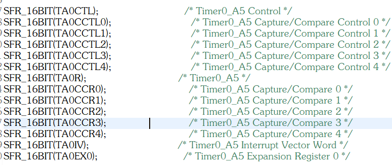
1.TA0CTL register is the total control register of timer A. relevant bits can be configured by writing words defined by macros
2.TA0CCTL0 register is the control register of the first capture / comparator under timer A. the corresponding functions can also be configured by writing relevant words.
3.TA0CCR0 register can determine how many times to time once by writing relevant values.
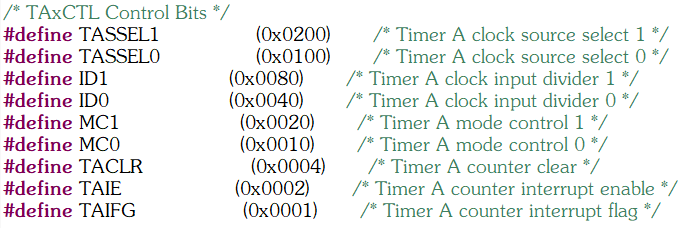
The configuration words corresponding to TA0CTL register can be configured by writing the words defined by these macros.
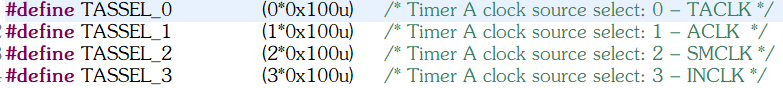
a.TASSELn bit can select the clock source of the timer (I generally choose SMCLK, which has a frequency with the master clock)
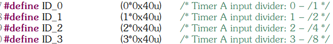
b. IDn bit can divide the frequency of the master clock. For example, if the frequency is divided by two, the 16Mhz master clock will become 8Mhz, and the maximum frequency is eight.
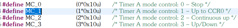
c. MCn bit can configure the functions corresponding to the register, which are stop count, increase count, continue count and increase / decrease count in order. PWM mode and timer mode can be increased by counting mode.
d. The taclr bit can clear the count value. It should be written to make the timer into the initial state at the beginning of configuration.
e. The TAIE bit can turn on the timer interrupt function.
f. The taifg bit will be automatically set to one when the timer interrupt is triggered.
Introduction to relevant functional bits of TA0CCTLn register
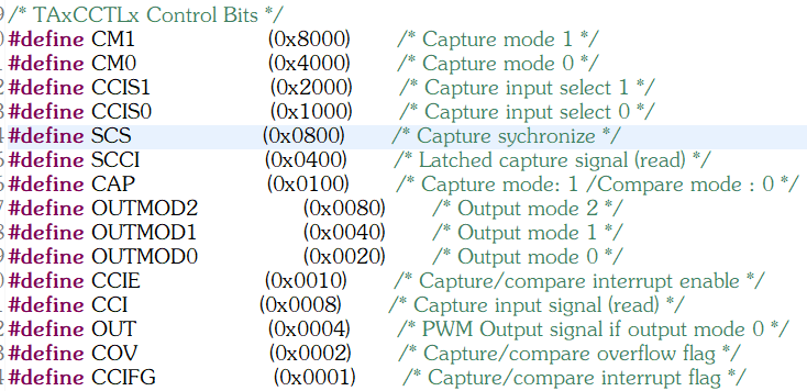
a. When used as a timer function, you only need to set CCIE, that is, turn on the comparator interrupt enable.
b. PWM sets OUTMOD_7, set to reset / set mode.
Other functional bits used as comparators / traps will not be introduced first.
Timer0_A5, 5 means that there are 5 capture / comparators. Two configuration routines will be given below. The PWM routine can observe the output of the corresponding pin through the oscilloscope.
Routine 1. Timer function
Value configuration formula corresponding to TA0CCR0:
Ta0ccr0 = 16m (clock frequency) /( 2 (default dichotomy) * 200(5ms corresponding frequency) )
If the corresponding frequency division is configured, the corresponding frequency division value needs to be removed
#include <msp430.h>
void initClockTo16MHz()
{
    UCSCTL3 |= SELREF_2;                      // Set DCO FLL reference = REFO
    UCSCTL4 |= SELA_2;                        // Set ACLK = REFO
    __bis_SR_register(SCG0);                  // Disable the FLL control loop
    UCSCTL0 = 0x0000;                         // Set lowest possible DCOx, MODx
    UCSCTL1 = DCORSEL_5;                      // Select DCO range 16MHz operation
    UCSCTL2 = FLLD_0 + 487;                   // Set DCO Multiplier for 16MHz
                                              // (N + 1) * FLLRef = Fdco
                                              // (487 + 1) * 32768 = 16MHz
                                              // Set FLL Div = fDCOCLK
    __bic_SR_register(SCG0);                  // Enable the FLL control loop

    // Worst-case settling time for the DCO when the DCO range bits have been
    // changed is n x 32 x 32 x f_MCLK / f_FLL_reference. See UCS chapter in 5xx
    // UG for optimization.
    // 32 x 32 x 16 MHz / 32,768 Hz = 500000 = MCLK cycles for DCO to settle
    __delay_cycles(500000);//
    // Loop until XT1,XT2 & DCO fault flag is cleared
    do
    {
        UCSCTL7 &= ~(XT2OFFG + XT1LFOFFG + DCOFFG); // Clear XT2,XT1,DCO fault flags
        SFRIFG1 &= ~OFIFG;                          // Clear fault flags
    }while (SFRIFG1&OFIFG);                         // Test oscillator fault flag
}

void time0Init(void)
{
    TA0CTL |= MC_1 + TASSEL_2 + TACLR;       //The clock is SMCLK, the counting mode is increased, and the counter is cleared at the beginning
    TA0CCTL0 = CCIE;            //Comparator interrupt enable
    TA0CCR0 = 40000;           //Interruption (cycle) 5ms
}

void GPIO_init(void){
    P4DIR |= BIT7;
}

void main(void){
    WDTCTL = WDTPW + WDTHOLD;                 // Stop WDT
    initClockTo16MHz();                        //Configure the system clock to 16Mhz
    GPIO_init();
    time0Init();
    _EINT();
    while(1){
    }

}

/************************Timer interrupt function********************************/
#if 1

#pragma vector = TIMER0_A0_VECTOR
__interrupt void Timer_A(void)
{
    P4OUT ^= BIT7;
}

#endif
Routine 2.PWM mode
The actual output frequency is mainly displayed by oscilloscope.
Which pins can be used to output PWM wave? Please see the built-in pin function diagram.
#include <msp430.h>
void initClockTo16MHz()
{
    UCSCTL3 |= SELREF_2;                      // Set DCO FLL reference = REFO
    UCSCTL4 |= SELA_2;                        // Set ACLK = REFO
    __bis_SR_register(SCG0);                  // Disable the FLL control loop
    UCSCTL0 = 0x0000;                         // Set lowest possible DCOx, MODx
    UCSCTL1 = DCORSEL_5;                      // Select DCO range 16MHz operation
    UCSCTL2 = FLLD_0 + 487;                   // Set DCO Multiplier for 16MHz
                                              // (N + 1) * FLLRef = Fdco
                                              // (487 + 1) * 32768 = 16MHz
                                              // Set FLL Div = fDCOCLK
    __bic_SR_register(SCG0);                  // Enable the FLL control loop

    // Worst-case settling time for the DCO when the DCO range bits have been
    // changed is n x 32 x 32 x f_MCLK / f_FLL_reference. See UCS chapter in 5xx
    // UG for optimization.
    // 32 x 32 x 16 MHz / 32,768 Hz = 500000 = MCLK cycles for DCO to settle
    __delay_cycles(500000);//
    // Loop until XT1,XT2 & DCO fault flag is cleared
    do
    {
        UCSCTL7 &= ~(XT2OFFG + XT1LFOFFG + DCOFFG); // Clear XT2,XT1,DCO fault flags
        SFRIFG1 &= ~OFIFG;                          // Clear fault flags
    }while (SFRIFG1&OFIFG);                         // Test oscillator fault flag
}

void PWMInit(void)
{

#if 1

    P2DIR |= BIT0;
    P2SEL |= BIT0;
    TA1CCTL1 |= OUTMOD_7; //Reset set mode
    TA1CTL |= TASSEL_2 + MC_1 + ID_3; //Set the clock source to SMCLK 16Mhz 8 frequency division
    TA1CCR0 = 400;            // 400:16Mhz/8/400≈5000hz
    TA1CCR1 = 200;            //The value is 200 when the duty cycle is 50%

#endif

}

void GPIO_init(void){
    P4DIR |= BIT7;
}

void main(void){
    WDTCTL = WDTPW + WDTHOLD;                 // Stop WDT
    initClockTo16MHz();                        //Configure the system clock to 16Mhz
    GPIO_init();
    PWMInit();
    _EINT();
    while(1){
        P4OUT |= BIT7; //Light up
    }

}