Realization of VGA display 8 color bar
Software used: Quartus II 13.1
Language used: Verilog HDL
On board chip: EP4CE6E22C8
Write in front
Since the FPGA foundation studied in school was based on VHDL (very high speed integrated circuit hardware description language), but most of them had forgotten and didn't want to start from scratch, so they studied and contacted FPGA again and wanted to use another HDL (hardware description language) closer to C language - that is, Verilog HDL.
VHDL has entity, architecture, configuration, package, and library.
-
entity mainly includes the Port declaration and establishes a black box model.
-
The architecture mainly includes the internal logic design at the behavior level to configure each process or state machine.
-
Library is used to reference the required library files. Often use the library file library ieee;
-
Package is used to reference the required package file. For example, if you want to use STD_ Logic (standard logic) type. The package in which the type is located shall be declared use IEEE std_ logic_ 1164.all;, Otherwise, an error will be reported; If behavior level modeling requires operator overloading, declare use IEEE std_ logic_ unsigned. All, if type conversion is required, convert the function conv from integer to logical vector type_ STD_ LOGIC_ Vector (begin, end), you need to reference use IEEE std_ logic_ arith. all
Of course, similar to VHDL, Verilog HDL also has a similar structure, such as module, procedural ` include (header file) corresponding to VHDL port, process and package. Therefore, Verilog HDL is not a problem if it is based on C language and VHDL language.
preparation
The book returns to the true story and understands the syntax of the language used, which is conducive to code writing and code reading.
We should learn more about VGA.
VGA interface
VGA interface is a D-type interface, which adopts asymmetric distribution connection mode, with a total of 15 pins. For users, its outgoing line commonly has five signals: red R, green G, blue B, line synchronization signal HS, field synchronization signal VS. HS and VS are used to process input analog signals and control the display timing of VGA in parallel, corresponding to Pin1, PIN2, PIN3, PIN13 and PIN14 respectively.
Is it a little abstract? The picture above here is the most direct and clear
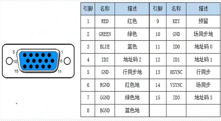
Of course, art students and Photoshop users should not be too unfamiliar with colors. Red, Green and Blue are the three primary colors. After different mixing and collision, they produce a colorful world and then display it on the screen. However, the internal output of the hardware is a digital signal, which can not be displayed on the VGA display screen. Therefore, digital analog converter (DAC) is required, The commonly used digital to analog conversion chip is ADV7125, which is the conversion of DAC signals of three 8-bit video signals.
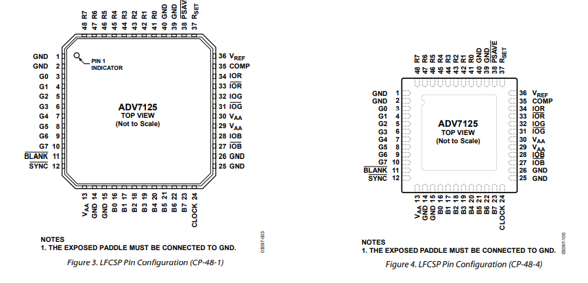
However, the chip overhead will be relatively large, so generally VGA video image signals are completed using a weight resistor network (as shown in the figure below)
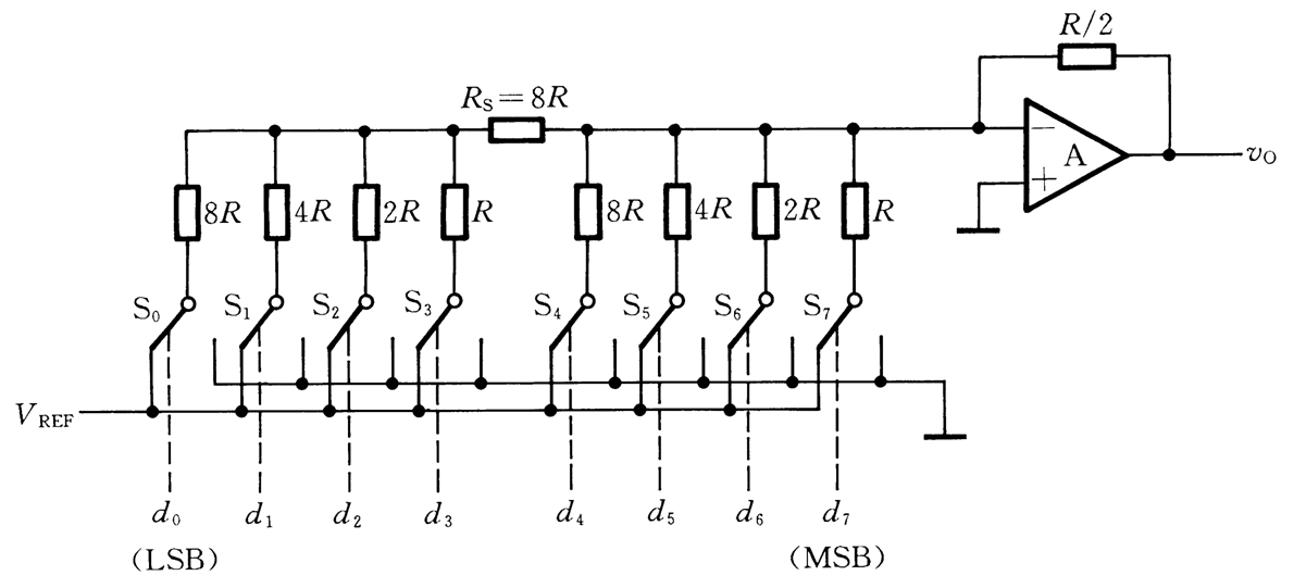
When R s = 8 R {R_s = 8R } Rs=8R, V o = − V r e f 2 8 D n {V_o = -\frac{V_{ref}}{2^8}D_n} Vo=−28VrefDn, D n yes high position ( M S B ) or low position ( L S B ) electric Resistance power heavy {D_n} is the high (MSB) or low (LSB) resistance weight Dn ¢ is the weight of high (MSB) or low (LSB) resistance
VGA timing
Understand the relevant knowledge of VGA interface and further understand the knowledge of VGA timing, because the writing code is generally based on timing. In terms of general industrial standards, 640* 480@60 The display is relatively stable and easy to grasp, so the following is based on 640* 480@60 About.
@Attention: 640* 480@60 , indicating that there are 307200 pixels in the row and column, and the rate of displaying one frame of image at the same time is 60MHz
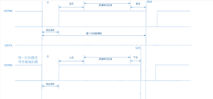
It can be seen from the above figure that the line scanning cycle is in pixels, which consists of line synchronization, trailing edge, image effective area and leading edge until the beginning of the next frame of image. When the scanning of one line is completed, the field scanning cycle starts, and the image effective area and lower edge are formed through field synchronization, upper edge and lower edge.
Start Coding
According to the previous explanation, you should understand the VGA display, so start Coding.
/*
* @author: lgdsmq
* @data:2021.12.26
* @modulename:VGA
* @header:include"vga_param.v"
*/
`include"vga_param.v"
module VGA(
clock	,
switch	,
out_RGB	,
hsync	,
vsync
);
input  clock		;    //System clock 50MHz
input  [1:0] switch	;	//Used to switch modes and display checkerboard

output [2:0] out_RGB;   //VGA output color
output  hsync		;   //VGA scan signal
output  vsync		;   //VGA field scan signal

reg [9:0]    hcount	;   //VGA line counter
reg [9:0]    vcount	;  //VGA field counter
reg [2:0]    data		;
reg [2:0]    h_dat		;
reg [2:0]    v_dat		;

reg   flag				;	//Flag bit
wire  hcount_ov			; 	//Overflow signal
wire  vcount_ov			;
wire  dat_act			;
wire  hsync				;
wire  vsync				;
reg  vga_clk			;

//Clock with frequency division operation of 25MHz
always @(posedge clock)
begin
vga_clk = ~vga_clk;
end

//************************VGA drive*******************************
//Row count
always @(posedge vga_clk)
begin
if (hcount_ov)// Clear if overflow
hcount <= 10'd0;
else
hcount <= hcount + 10'd1;
end
assign hcount_ov = (hcount == hpixel_end);
//Field count
always @(posedge vga_clk)
begin
if (hcount_ov)
begin
if (vcount_ov)
vcount <= 10'd0;
else
vcount <= vcount + 10'd1;
end
end
assign  vcount_ov = (vcount == vline_end);
//Determine whether it is in the valid data area
assign dat_act =    ((hcount >= hdat_begin) && (hcount < hdat_end))
&& ((vcount >= vdat_begin) && (vcount < vdat_end));
assign hsync = (hcount > hsync_end);
assign vsync = (vcount > vsync_end);
assign disp_RGB = (dat_act) ?  data : 3'h00;

//************************VGA display processing operation*******************************
always @(posedge vga_clk)
begin
case(switch[1:0])
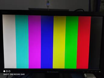
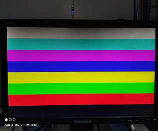
2'd0: data <= h_dat;      //Row data
2'd1: data <= v_dat;      //Column data
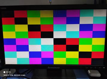
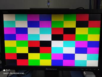
2'd2: data <= (v_dat ^ h_dat); //Chessboard
2'd3: data <= (v_dat ~^ h_dat); //Transposed chessboard
endcase
end

always @(posedge vga_clk)  //Line color bar counting sequence
begin
if(hcount < 223)
v_dat <= 3'h7;
else if(hcount < 303)
v_dat <= 3'h6;
else if(hcount < 383)
v_dat <= 3'h5;
else if(hcount < 463)
v_dat <= 3'h4;
else if(hcount < 543)
v_dat <= 3'h3;
else if(hcount < 623)
v_dat <= 3'h2;
else if(hcount < 703)
v_dat <= 3'h1;
else
v_dat <= 3'h0;
end

always @(posedge vga_clk)  //Column color bar counting sequence
begin
if(vcount < 94)
h_dat <= 3'h7;
else if(vcount < 154)
h_dat <= 3'h6;
else if(vcount < 214)
h_dat <= 3'h5;
else if(vcount < 274)
h_dat <= 3'h4;
else if(vcount < 334)
h_dat <= 3'h3;
else if(vcount < 394)
h_dat <= 3'h2;
else if(vcount < 454)
h_dat <= 3'h1;
else
h_dat <= 3'h0;
end

endmodule
Header file of timing parameters (vga_param.v)
`ifndef __VGA_PARAM_
`define __VGA_PARAM_640_480_60MHz
`define hsync_end    10'd95
`define hdat_begin   10'd143
`define hdat_end     10'd783
`define hpixel_end   10'd799
`define vsync_end 	 10'd1
`define vdat_begin   10'd34
`define vdat_end     10'd514
`define vline_end  	 10'd524
`endif
The introduction of header file can improve the portability of code, and display the code style of the file more succinctly and easily understood
The results show that
Write at the end
FPGA's first composition, there are still deficiencies, I would like to encourage you.