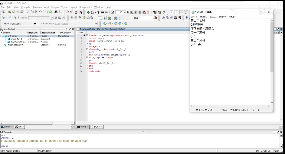
Part I: introduction of this experiment
This brings you three experiments. The following is the code of this experiment
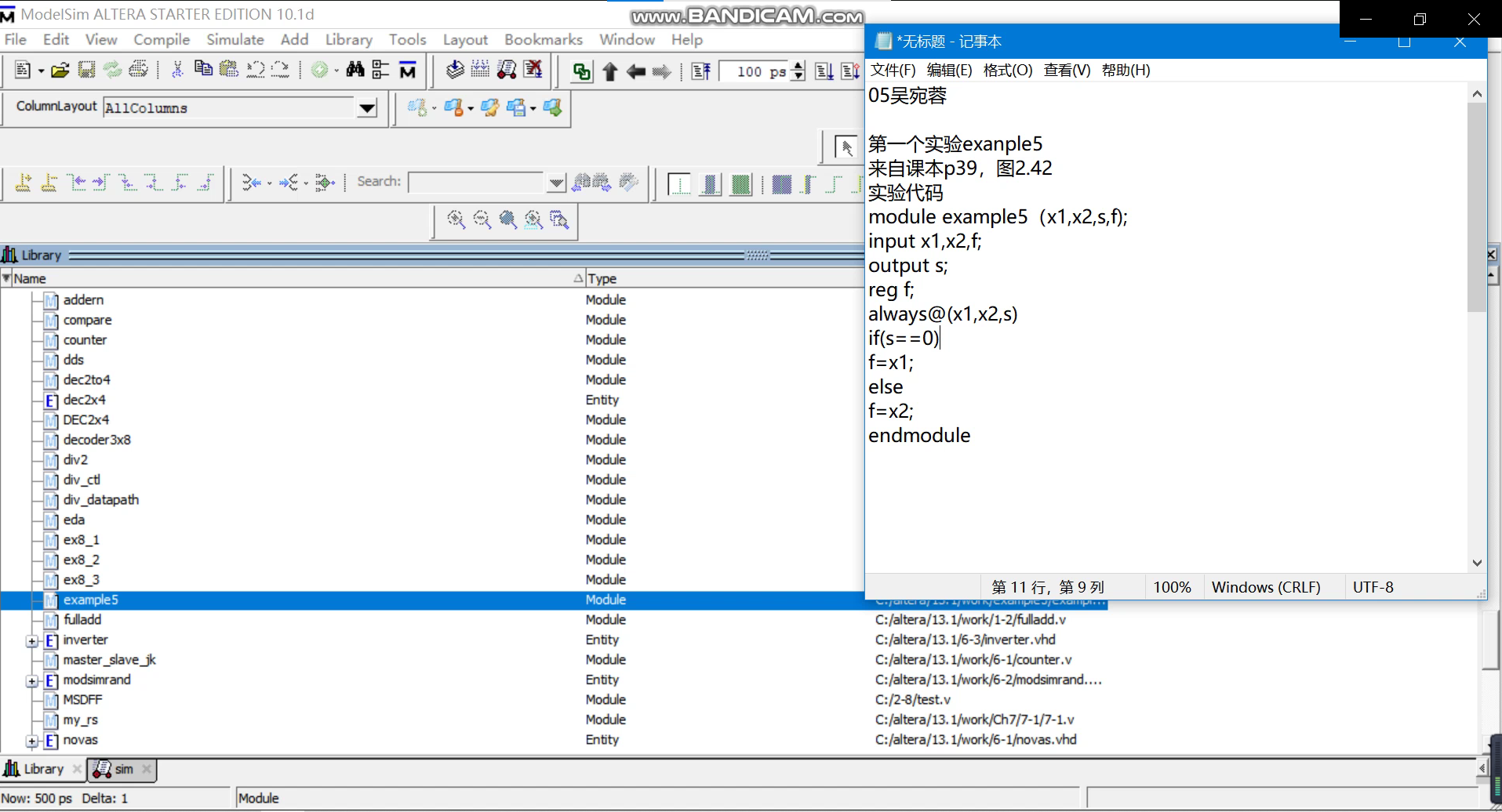
First experiment
From p39 figure 2.42 in the textbook
Behavior level description circuit code language
module example5(x1,x2,s,f);
input x1,x2,s;
output f;
reg f;
always @(x1,x2,s)
if (s==0)
f=x1;
else
f=x2;
endmodule
The second experiment
From Verilog HDL advanced design (Second Edition)
p159 figure 6.16
Unintentional synthesis of latches
First file: or4 experimental principle file
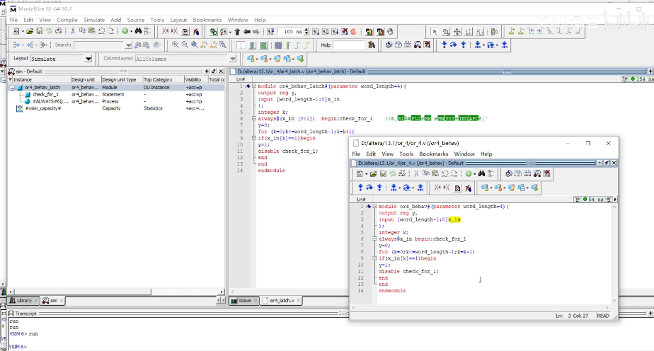
module or4_behav#(parameter word_length=4)(
output reg y,
input [word_length-1:0]x_in
);
integer k;
always@x_in begin:check_for_1
y=0;
for (k=0;k<=word_length-1;k=k+1)
if(x_in[k]==1)begin
y=1;
disable check_for_1;
end
end
endmodule
The second file: or4#; latch
module or4_behav_latch#(parameter word_length=4)(
output reg y,
input [word_length-1:0]x_in
);
integer k;
always@(x_in [3:1])  begin:check_for_1    //Incomplete sensitive table
y=0;
for (k=0;k<=word_length-1;k=k+1)
if(x_in[k]==1)begin
y=1;
disable check_for_1;
end
end
endmodule
The third experiment
Verilog HDL simulation design (version 2)
Chapter 11 Experiment 6
First file: dds experimental principle code
module dds(clk,reset,div,choose,data);
input [5:0] div;
input [1:0] choose;
input clk,reset;
output [7:0] data;
wire [7:0]data;
reg [5:0] addr,address;
reg [5:0] i;
reg clkdiv;
function [7:0] rom;
input [5:0]address;
begin
case (address)
     0 : rom = 0;
	  1 : rom = 4;
	  2 : rom = 12;
	  3 : rom = 21;
	  4 : rom = 25;
	  5 : rom = 21;
	  6 : rom = 12;
	  7 : rom = 4;
	  8 : rom = 20;
	  9 : rom = 20;
	  10 : rom = 20;
	  11 : rom = 20;
	  12 : rom = 1;
	  13 : rom = 1;
	  14 : rom = 1;
	  15 : rom = 1;
	  16 : rom = 0;
	  17 : rom = 5;
	  18 : rom = 10;
	  19 : rom = 15;
	  20 : rom = 20;
	  21 : rom = 25;
	  22 : rom = 30;
	  23 : rom = 35;
	  24 : rom = 35;
	  25 : rom = 30;
	  26 : rom = 25;
	  27 : rom = 20;
	  28 : rom = 15;
	  29 : rom = 10;
     30 : rom = 5;
     31 : rom = 0;
	  default :rom = 10'hxx;
	  endcase
	  end
	  endfunction
	  assign data = rom(address);
	  endmodule
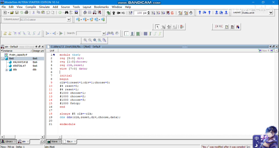
The second file: tbs6 experimental test code
module tbs6;
reg [5:0] div;
reg [1:0]choose;
reg clk,reset;
wire [7:0] data;

initial
begin
clk=0;reset=1;div=1;choose=0;
#4 reset=0;
#4 reset=1;
#1000 choose=1;
#1000 choose=2;
#1000 choose=3;
#1000 $stop;
end

always #5 clk=~clk;
dds dds(clk,reset,div,choose,data);

endmodule
Part II: introduction to the operation of the experiment
The first experiment: code description of behavior level language
Operation of the first experiment: code details of behavior level description language circuit
Step 1: add the file to the library of modelsim and open it
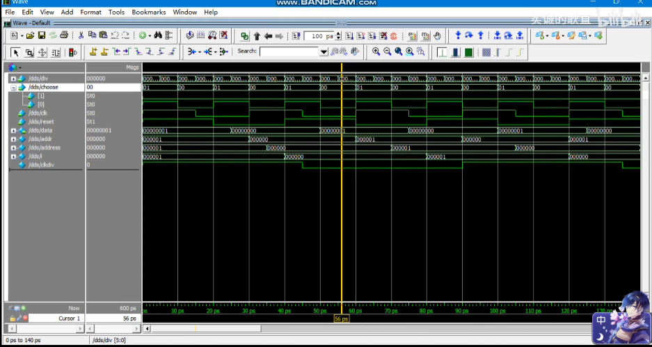
Step 2: the waveform of the experiment is simulated. The frequency of the experiment is 100ns and the parameter is 10ps
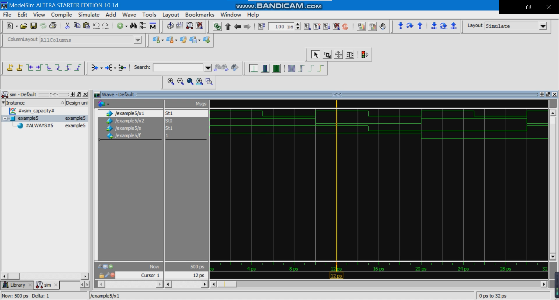
We will find that the result of our experiment is a timing chart with periodic changes
For detailed introduction, please enter my video: Explanation of textbook experiment
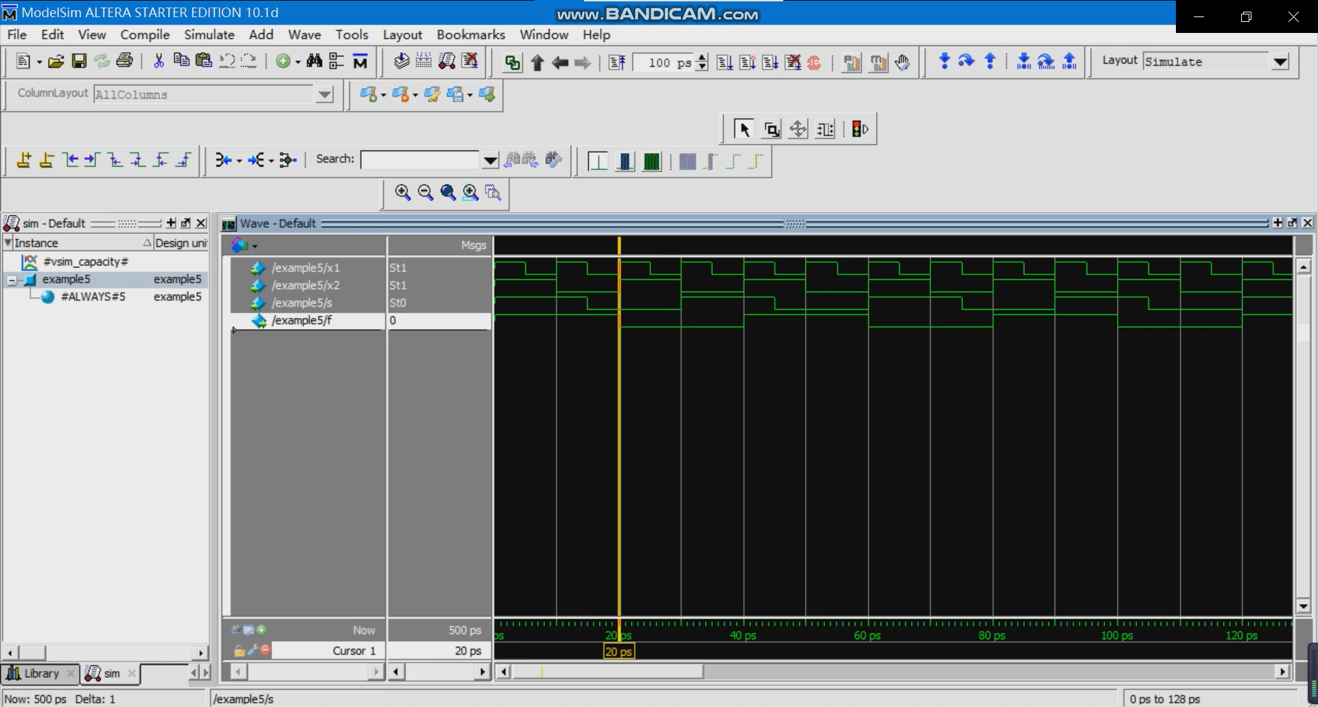
The second experiment: unintentional synthesis of latch
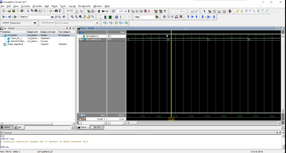
Step 1: open a file or4 in the library of modelsim
Step 2: the experiment is carried out to the waveform, the frequency is 100ns, and the increment of 10*n is adopted for each value
Step 3: use the method in step 1 to open our or4_latch file
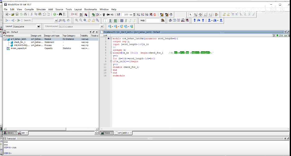
At this point, make a code comparison
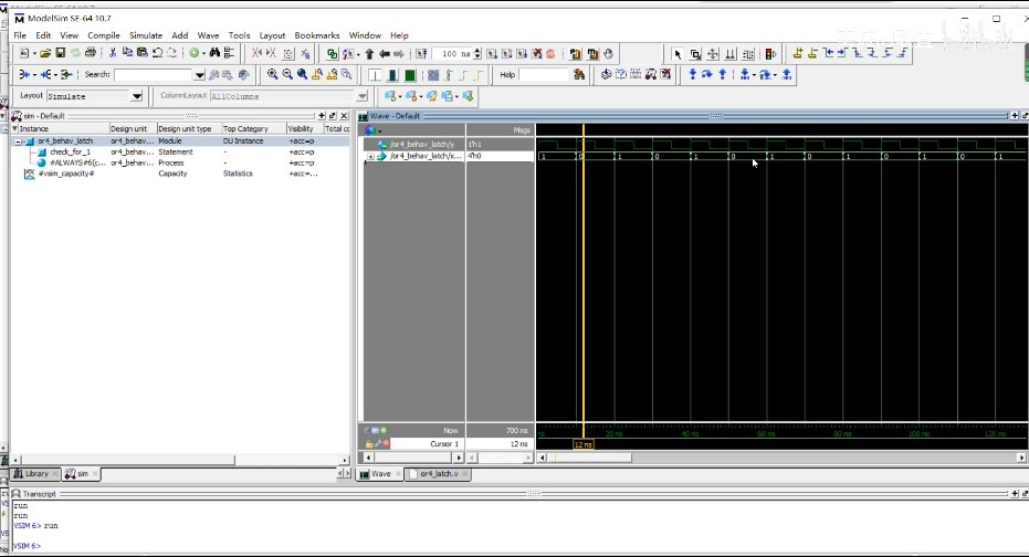
Step 4: observe the change of waveform diagram and analyze the simulation diagram
The detailed introduction will be in my video: Unintentional synthesis of latches
The third experiment: Experiment 6 "signal generator design"
Step 1: open the dds experiment principle file of the experiment in the library of modelsim
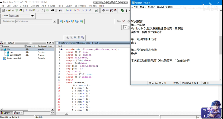
Step 2: after analyzing the experimental code, we conduct experimental simulation
Step 3: use the first step to open our tbs6 experimental test code
Step 4: simulate the test code and get the following simulation diagram
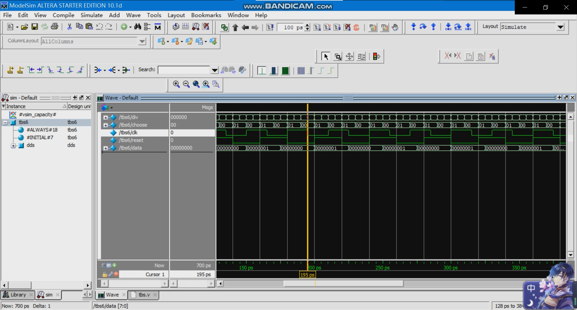
For detailed explanation, please enter my video: Signal generator design
Part III: experimental summary
Through the systematic study of this semester, the design of digital logic circuit for several days has ended. I feel deeply in the process of learning, design and signal generator simulation in these days. It gives me a concrete understanding of abstract theory. Through the design of function signal generator, I also deeply realized the importance and authenticity of the sentence "integrating theory with practice".
At the same time, in this experiment, I understand why the teacher always let us operate, so that we can understand how to use the knowledge to solve practical problems. For the design of this experiment, we had to review the previous knowledge, and began to check the information on the Internet, and occasionally discussed with the students. This is another review and application of our previous knowledge. In the experiment, code errors can make people collapse most, but these problems are solved with the help of students. When you see those waveforms, you will feel a special sense of achievement. Secondly, this course design has improved the level of cooperation between my classmates and me, made us cooperate more tacitly, realized that success comes from sweat and realized that the results are hard won.
Through this practical operation, I also deeply understand that only by combining the theoretical knowledge in the textbook with practice, constantly summarizing and refining, and repeatedly thinking about the experience and lessons in practice, can I really digest it into my own knowledge.
Experimental tools: 13.1 QuartusII and modelsim10 1D and modelsim10 7d