In the introduction of Altera's SCFIFO core on the Internet, it is mentioned that it can support simultaneous reading and writing, but the specific simulation situation is not seen. There is no clear description of this in Altera's official ug (or I didn't read the document carefully). Therefore, the problem is simulated by modelsim, and the simulation situation is recorded here for discussion.
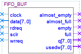
Firstly, a 256B SCFIFO core is generated, and its main parameters are as follows:
defparam
		scfifo_component.add_ram_output_register = "ON",
		scfifo_component.almost_empty_value = 64,
		scfifo_component.almost_full_value = 128,
		scfifo_component.intended_device_family = "Cyclone III",
		scfifo_component.lpm_numwords = 256,
		scfifo_component.lpm_showahead = "OFF",
		scfifo_component.lpm_type = "scfifo",
		scfifo_component.lpm_width = 8,
		scfifo_component.lpm_widthu = 8,
		scfifo_component.overflow_checking = "ON",
		scfifo_component.underflow_checking = "ON",
		scfifo_component.use_eab = "ON";
The generated module shape is shown in the figure below.
Write the test code as follows
`timescale 1ns / 1ns
module fifo_buf_tb;
	reg	  hclk;
	reg	[7:0]  data;
	reg	  rdreq;
	reg	  sclr=0;
	reg	  wrreq;

	wire	  almost_empty;
	wire	  almost_full;
	wire	  empty;
	wire	  full;
	wire	[7:0]  q;
	wire	[7:0]  usedw;

FIFO_BUF	DUT (
	.clock ( hclk ),
	.data ( data ),
	.rdreq ( rdreq ),
	.sclr ( sclr ),
	.wrreq ( wrreq ),
	.almost_empty ( almost_empty ),
	.almost_full ( almost_full ),
	.empty ( empty ),
	.full ( full ),
	.q ( q ),
	.usedw ( usedw )
	);

//20MHz high clock
  initial
  begin
   hclk  = 1'b1  ;
   forever
	  #25  hclk  = !hclk  ;
  end

 //Update data every 1us, and add 1 for each update
 initial
 begin
	data=1;
	forever
		#1000	data=data+1;
 end

//Give a wrreq signal with high clock period
initial
begin
	wrreq=0;
	forever
	begin
		#(0) wrreq=1;
		#50	wrreq=0;
		#(1000-50) ;
	end
end

//After writing 64 bytes into FIFO, read test shall be carried out
initial
begin
	rdreq=0;
	forever
	begin
		#0 rdreq=(usedw>64?1:0);
		#50	rdreq=0;
		#(1000-50) ;
	end
end

//Start Time = 0 ns, End Time = 1ms
initial
	#1000000 $stop;
endmodule
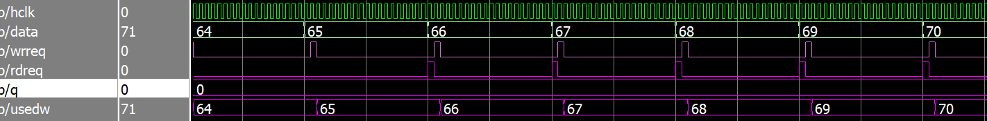
The simulation results of modelsim are shown in the figure below.
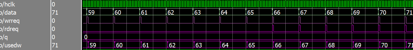
It can be seen that when the jump of input data occurs simultaneously with wrreq and rdreq, the data in SCFIFO cannot be read normally, but it is very strange that after reducing the operation frequency of wrreq and rdreq, the jump edges of the three are still synchronous, but the reading is normal.
Relevant codes are adjusted as follows
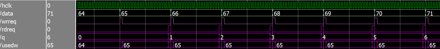
//Give a wrreq signal with high clock period
initial
begin
	wrreq=0;
	forever
	begin
		#(1000) wrreq=1; 	// The operating frequency of wrreq is reduced by half
		#50	wrreq=0;
		#(1000-50) ;
	end
end

//After writing 64 bytes into FIFO, read test shall be carried out
initial
begin
	rdreq=0;
	forever
	begin
		#1000 rdreq=(usedw>64?1:0); 	 Reduce the operating frequency of rdreq by half
		#50	rdreq=0;
		#(1000-50) ;
	end
end
The simulation results are shown in the figure below.
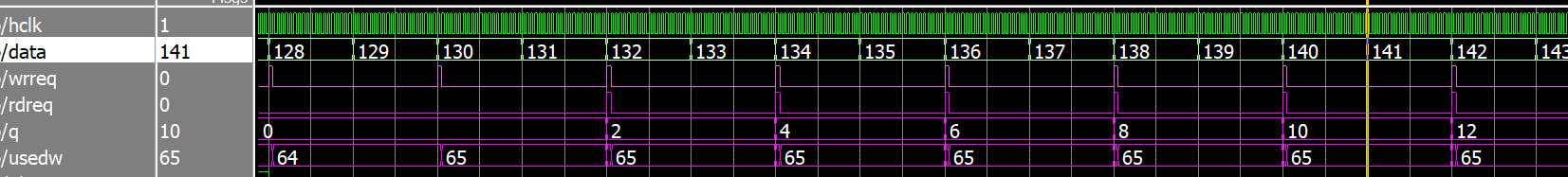
It can be seen that the simultaneous reading and writing of SCFIFO is normal at this time, but the reason is hard to understand.
Continue to discuss the scenario that SCFIFO cannot read and write at the same time. At first, it was thought that it was caused by the jump of wrreq and data at the same time. Modify the test code to make wrreq advance and error one high clock cycle respectively. The simulation results are shown in the figure below.
It can be seen that whether wrreq is in advance or after error has no impact on the simulation results, and the data in SCFIFO cannot be read normally.
Adjust the test mode, fix the jump of wrreq and data at the same time, and adjust the generation time of rdreq. The simulation results are shown in the figure below.
It can be seen that as long as rdreq does not jump at the same time with the input data, the data in SCFIFO can be read out normally.
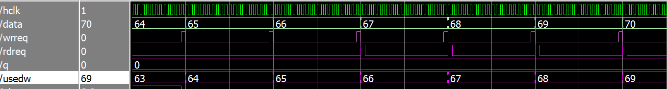
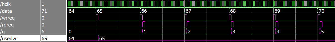
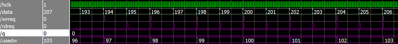
Continue to conduct univariate test for the problem of reading and writing frequency, and only reduce the reading frequency. The simulation results are shown in the figure below (the reading trigger condition is changed to usedw > 96).
At this time, the simultaneous reading and writing of SCFIFO is normal.
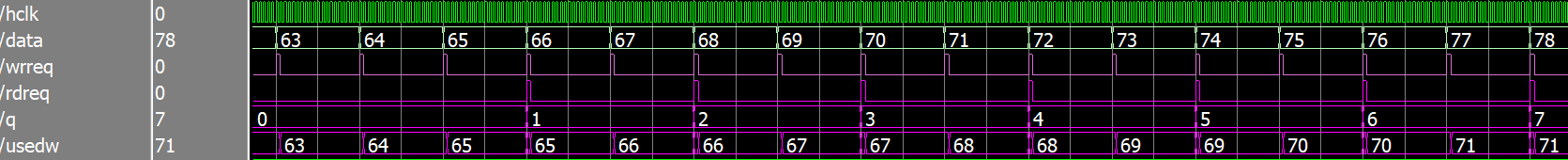
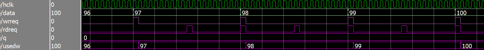
Reduce the write frequency for simulation, and the results are shown in the figure below.
At this time, the data in SCFIFO cannot be read normally.
Encryption reading frequency, and the simulation results are shown in the figure below.
At this time, the reading of SCFIFO is abnormal. It is speculated that the output of SCFIFO is abnormal because rdreq is in the same frequency and phase as the input data, and other rdreq signals cannot work normally.
It can be concluded from the above test that when the period and jump edge of rdreq signal are completely consistent with the input data, the data in SCFIFO cannot be read out normally.
Despite this conclusion, the mechanism of the problem is still unclear and whether it has anything to do with the implementation mechanism of SCFIFO core. No description was found in altera's documentation. Therefore, the correctness of the conclusion can not be fully guaranteed, and all great gods are expected to give guidance.