Memory reading and writing experiment:
Assign BCD codes 75H and 35H to 30H and 31H units of RAM respectively, try to add the two numbers, and the difference of BCD is sent to 32H unit.
(description):
Because the decimal adjustment instruction of MCS-51 is not suitable for subtraction, subtraction can be changed into addition: the subtraction subtraction is changed into the complement of subtraction + subtraction, where the complement of subtraction = the modulus subtraction of BCD code. Finally, the decimal addition instruction is used to send the complement of subtracted + subtracted to memory A and then store it in 32H unit.
(flow chart):
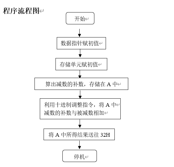
	ORG	0000H
	LJMP	START
	ORG	0020H
START:	MOV	R0,#30H
	MOV	R1,#31H
	MOV	30H,#72H
	MOV	31H,#35H
	MOV	A,#9AH
	SUBB	A,@R1
	ADD	A,@R0
	DA	A
	MOV	32H,A
	SJMP	$
	END
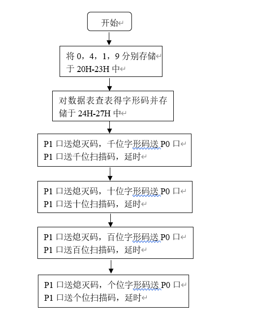
Parallel port experiment:
Using the two interfaces of single chip microcomputer to drive the four in one LED nixie tube circuit, it is required to directly display "0, 4, 1, 9" in RAM20H-23H from right to left on the nixie tube.
(description):
The data variable to be displayed is stored in 20H-23H of RAM, and the corresponding font code is stored in 24H-27H of RAM. The font code corresponding to the variable is obtained by looking up the table. According to the characteristics of the circuit, the bit driving level is low and effective. The DELAY of the subroutine DELAY determines the lighting time of each nixie tube. The DELAY time can be increased by modifying the DELAY parameters in DELAY, so as to observe the effect of dynamic display.
(flow chart):
ORG	0000H
	LJMP	START
	ORG	0030H
START:	MOV	SP,#60H
	MOV	A,#00H
	MOV	R0,#20H
	MOV	@R0,A
	MOV	A,#4
	INC	R0
	MOV	@R0,A
	INC	R0
	MOV	A,#1
	MOV	@R0,A
	INC	R0
	MOV	A,#9
	MOV	@R0,A
	MOV	R0,#20H
	MOV	R1,#24H
	MOV	R2,#4
	MOV	DPTR,#LEDGY
LOOP1:	MOV	A,@R0
	MOVC	A,@A+DPTR
	MOV	@R1,A
	INC	R0
	INC	R1
	DJNZ	R2,LOOP1
LOOP2:	MOV	P1,#0FFH
	MOV	P0,24H
	MOV	P1,#0EFH
	LCALL	DELAY
	MOV	P1,#0FFH
	MOV	P0,25H
	MOV	P1,#0DFH
	LCALL	DELAY
	MOV	P1,#0FFH
	MOV	P0,26H
	MOV	P1,#0BFH
	LCALL	DELAY
	MOV	P1,#0FFH
	MOV	P0,27H
	MOV	P1,#07FH
	LCALL	DELAY
	SJMP	LOOP2
LEDGY:	DB	0C0H,0F9H,0A4H,0B0H,99H,92H,82H,0F8H
	DB	80H,90H,88H,83H,0C6H,0A1H,86H,8EH
DELAY	PUSH	00H
	PUSH	01H
	MOV	R1,#00H
LOOP3:	MOV	R0,#06H
	DJNZ	R0,$
	DJNZ	R1,LOOP3
	POP	01H
	POP	00H
	RET
	END
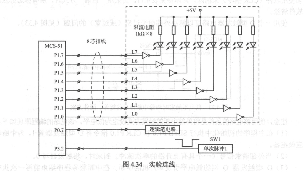
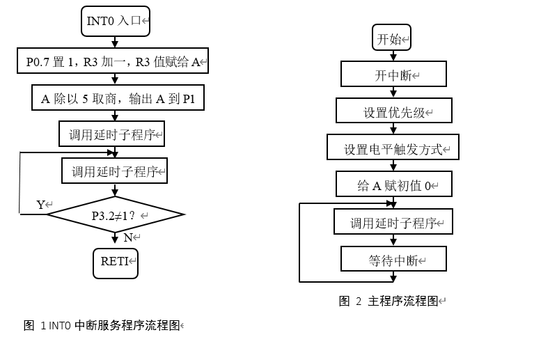
External interrupt test:
Design a counter, use the interrupt program to complete the function of displaying it every five times, and the counter is initially cleared. Use the "logic pen" circuit to display P0 7 status: if P0.05 If the level of 7 changes continuously, it indicates that the system is executing the main program without interruption; If P0.05 7 becomes a fixed high level, indicating that the system enters an interrupt.
(description):
Set / INT0 interrupt entry, and set P0 in the interrupt service program 7 is set to 1. In the interrupt program, every time an interrupt is accepted, add one to R3 and transfer the data in R3 to A. divide a by 5 to detect whether the interrupt is accepted for five times. When it is reached, add the counter and display it together. A delay program is added for software anti shake every time the reading is interrupted.
(circuit diagram):
(flow chart):
ORG 0000H
	LJMP START
	ORG 0003H
	LJMP INT_0
	ORG 0030H
START: 	MOV SP,#60H
	MOV TCON,#00H
	MOV R3,#00H
	MOV A,R3
	SETB EX0 ;
	SETB EA ;Allow interrupt
LOOP1:	MOV P1,A
	CPL P0.7
	LCALL DELAY
	SJMP LOOP1
INT_0: 	PUSH PSW
	SETB P0.7
	INC R3
	MOV A,R3
	MOV B,#5
   DIV A B
	MOV P1,A
	LCALL DELAY
	JNB P3.2,$
	LCALL DELAY
	POP PSW
	RETI
DELAY:	PUSH 01H
	PUSH 02H
	MOV R4,#12H
LOOP2:	NOP
	DJNZ R4,LOOP2
	MOV R1,#00H
DELAY1:	MOV R2,#00H
	DJNZ R2,$
	DJNZ R1,DELAY1
	POP 02H
	POP 01H
	RET
	END
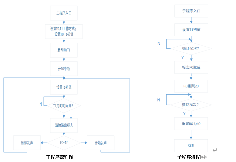
Timing counter experiment:
T0 and T1 are respectively used to realize the procedure that the buzzer whistles at the frequency of 1Khz for 2s, stops for 1s and makes sound circularly.
(description):
Use the timer / counter T1 and query method to set the initial value 0FE33H and control the sound frequency of 1KHZ; Using the timer / counter T0 and the interrupt method, set the initial value 4BFCH, interrupt once every 50MS, and use the cycle to achieve the second timing effect of timing 2s and stopping 1s.
(circuit diagram):

(flow chart):
ORG	0000H
	LJMP	START
	ORG	000BH
	LJMP	INT_0
	ORG	0030H
START:
	MOV	SP,#60H
	MOV	TMOD,#11H 		; Both T0 and T1 work in mode 1
	MOV	TL0,#0FCH
	MOV	TH0,#4BH 		; T0 sets the initial value 4BFCH and interrupts once every 50MS
	MOV	TL1,#033H
	MOV	TH1,#0FEH 		; T1 sets the initial value 0FE33H and controls the sound frequency of 1KHZ
	SETB	TR1
	SETB	TR0
	SETB	EA
	SETB	ET0
	MOV	A,#00H
	MOV	R0,#forty 			; 40 cycles
LOOP:
	CJNE	A,#00H,DOWN
	JNB	TF1,$			;Use query method
	CLR	TF1
	MOV	TL1,#033H
	MOV	TH1,#0FEH
	JB	F0,DOWN
	CPL	P1.1

DOWN:	SJMP	LOOP

INT_0:	PUSH	PSW			;Use interrupt method
	MOV	TL0,#0FCH
	MOV	TH0,#4BH
	DJNZ	R0,EXIT
	MOV	R0,#twenty 			; Cycle 20 times
	CJNE	A,#00H,TURN
	MOV	A,#01H
	SJMP	EXIT

TURN:	MOV	A,#00H
	MOV	R0,#40

EXIT:	POP	PSW
	RETI
	END
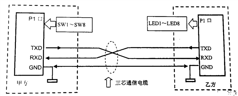
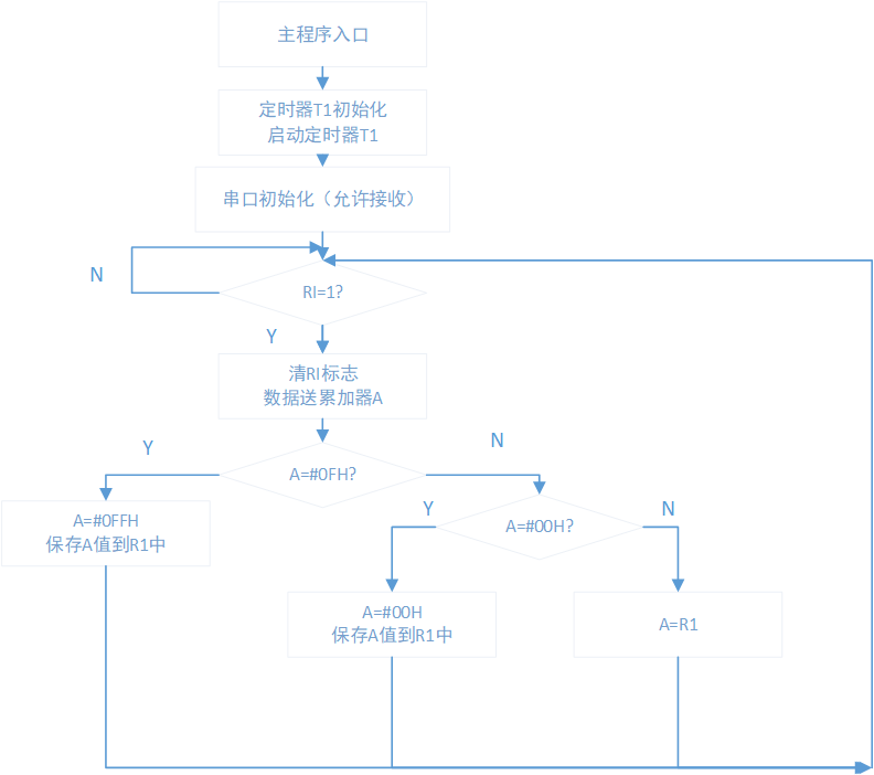
TLC549 serial AD conversion experiment and serial port experiment
Connect LED 1 ~ LED8 with P1 port in order to display the data received from the serial port. When the data received by the serial port is FF0FH, all the lights are on; When the data received by the serial port is FF00H, all the lights are off; When the serial port accepts data as other data, it maintains the previous data state.
(description):
Timer T1 works in mode 2, sets the initial baud rate to 9600HZ, clears the flag after receiving the data, first judges whether the data is 0FH, if so, assigns 0FFH to A and outputs it to make the lamp fully on; If not, judge whether it is 00H. If so, assign 00H to A and output it to turn off all the lights. If not, output the last saved R1 value to keep the lights as they are.
(circuit diagram):
(flow chart):
ORG	0030H
START:
	MOV	TMOD,#20H
	MOV	TL1,#0FDH 	; Initial value of sending timing
	MOV	TH1,#0FDH
	MOV	PCON,#00H
	SETB	TR1
	CLR	RI
	MOV	SCON,#50H 	; Serial interface mode 1 (acceptable)
LOOP1:
	JNB	RI,LOOP1		;Judge whether data is received
	CLR	RI		;Clear the accept flag after receiving data
	MOV	A,SBUF		;Data transmission accumulator A
	CJNE	A,#0FH,ZERO 	; Determine whether it is the maximum value

MAX:	MOV	A,#0FFH 		; Assign 0ffh to A
	MOV	R1,A
	MOV	P1,A		;from P1 Port output
	SJMP	LLL

ZERO:
	CJNE	A,#00H,DOWN 	; Judge whether it is 0
	MOV	A,#00H		;towards A Fu#00H
	MOV	R1,A
	MOV	P1,A
	SJMP	LLL

DOWN:	MOV	A,R1		;If the input data is other values, the previous data will be maintained
	MOV	P1,A
	SJMP	LLL

LLL:	SJMP	LOOP1
	END
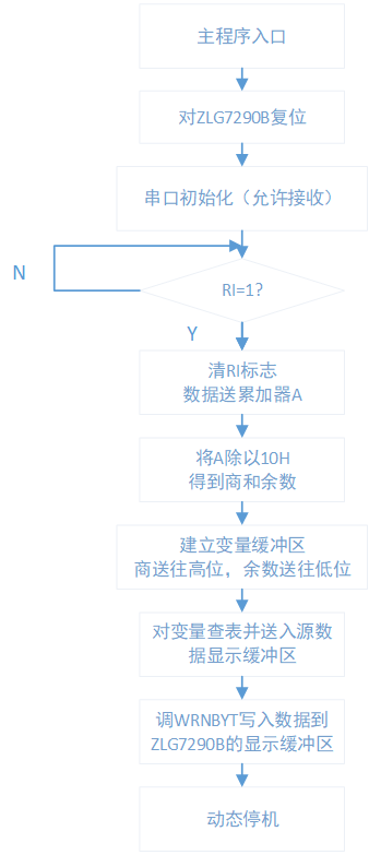
ZLG7290B dynamic display experiment:
Connect LED 1 ~ LED8 with P1 port in order to display the data received from the serial port. When the data received by the serial port is FF0FH, all the lights are on; When the data received by the serial port is FF00H, all the lights are off; When the data received by the serial port is other data, the previous data state is maintained.
(description):
The binary number to be displayed obtained from the original variable buffer is obtained by receiving data through serial port. Divide the two hexadecimal digits obtained from the serial port by 10H, and send the quotient to 31H as the high order; The remainder is sent to 30H for low order, so that the data can be correctly displayed on the nixie tube
(flow chart):
SDA BIT P1.0 SCL BIT P1.1 WSLA EQU 070H RSLA EQU 071H ORG 0000H LJMP START ;main program ORG 0030H START: MOV SP,#60H CLR P1.7 ;ZLG7290B reset MOV TMOD,#20H MOV TH1,#0fdh MOV TH1,#0fdh ; Initial value of sending timing MOV PCON,#00h SETB TR1 CLR RI MOV SCON,#50H ; Serial interface mode 1 (acceptable) LOOP1: JNB RI,LOOP1 ;Judge whether data is received CLR RI ;Clear the accept flag after receiving data MOV A,SBUF ;Data transmission accumulator A SETB P1.7 MOV B,#10H DIV AB MOV R4,A MOV A,B MOV R3,A ;Divide by 10 H,Get quotient and remainder MOV 30H,R3 MOV 31H,R4 ;The quotient is sent to the high position and the remainder is sent to the low position LCALL DELAY MOV DPTR,#LEDSEG ; Start looking up the variable table CLR A MOV R7,#02H MOV R0,#20H MOV R1,#30H LOOP1: MOV A,@R1 MOVC A,@A+DPTR ;Look up the corresponding font code in the table MOV @R0,A ;Send buffer INC R1 INC R0 DJNZ R7,LOOP1 MOV R7,#02H MOV R0,#20H MOV R2,#10H MOV R3,#WSLA LCALL WRNBYT SJMP LOOP LEDSEG: DB 0FCH,60H,0DAH,0F2H,66H,0B6H,0BEH,0E4H;60H-61H DB 0FEH,0F6H,0EEH,3EH,9CH,7AH,9EH,8EH DELAY: PUSH 00H PUSH 01H MOV R0,#00H DELAY1: MOV R1,#00H DJNZ R1,$ DJNZ R0,DELAY1 POP 01H POP 00H RET ;The following are subroutines ;******************************************************************* ;[Prompt] the following procedure is performed when the system clock is 12 MHZ(Or 11.0592MHZ),Namely NOP The command is about 1 microsecond. ;(1)Multibyte write operation subroutine with internal unit address WRNBYT ;******************************************************************* ;Universal I2C Communication subroutine (multi byte write operation) ;Entry parameters R7 Number of bytes,R0 Source block header address ; R2 Slave device internal sub address;R3 Peripheral device address (write) ;Related subroutineWRBYT,STOP,CACK,STA ;******************************************************************* WRNBYT: PUSH PSW PUSH ACC WRADD: MOV A,R3 ;Take the address of peripheral devices (including r/w=0) LCALL STA ;Send start signal S LCALL WRBYT ;Send peripheral address LCALL CACK ;Detect the response signal of peripheral devices JB F0,WRADD ;If the answer is not correct, return to start again MOV A,R2 LCALL WRBYT ;Send internal register header address LCALL CACK ;Detect the response signal of peripheral devices JB F0,WRADD ;If the answer is not correct, return to start again WRDA: MOV A,@R0 LCALL WRBYT ;Send peripheral address LCALL CACK ;Detect the response signal of peripheral devices JB F0,WRADD ;If the answer is not correct, return to start again INC R0 DJNZ R7,WRDA LCALL STOP POP ACC POP PSW RET ;******************************************************************* ;(2)Multibyte read operation subroutine with internal unit address RDNBYT ;******************************************************************* ;Universal I2C Communication subroutine (multi byte read operation) ;Entry parameters R7 Number of bytes; ;R0 The first address of the target data block; R2 Slave device internal sub address; ;R3 Device address (write); R4 Device address (read) ;Related subroutineWRBYT,STOP,CACK,STA,MNACK ;******************************************************************* RDNBYT: PUSH PSW PUSH ACC RDADD1:LCALL STA MOV A,R3 ;Write address LCALL WRBYT ;Send peripheral address LCALL CACK ;Detect the response signal of peripheral devices JB F0,RDADD1 ;If the answer is not correct, return to start again MOV A,R2 ;Get internal address LCALL WRBYT ;Send peripheral address LCALL CACK ;Detect the response signal of peripheral devices JB F0,RDADD1 ;If the answer is not correct, return to start again LCALL STA MOV A,R4 ;Get device address (read) LCALL WRBYT ;Send peripheral address LCALL CACK ;Detect the response signal of peripheral devices JB F0,RDADD1 ;If the answer is incorrect, return to start again RDN: LCALL RDBYT MOV @R0,A DJNZ R7,ACK LCALL MNACK LCALL STOP POP ACC POP PSW RET ACK: LCALL MACK INC R0 SJMP RDN ;********************************************************************** ;(3)I2C Each signal subroutine ;********************************************************************** ; Start signal subroutine S ;********************************************************************** STA: SETB SDA ;Start signal S SETB SCL NOP ;Generate 4.7US delayed NOP NOP NOP NOP CLR SDA NOP ;Generate 4.7US delayed NOP NOP NOP NOP CLR SCL RET ;********************************************************************** ; Stop signal subroutine P ;********************************************************************** STOP: CLR SDA ;Stop signal P SETB SCL NOP ;Generate 4.7US delayed NOP NOP NOP NOP SETB SDA NOP ;Generate 4.7US delayed NOP NOP NOP NOP SETB SCL ;Release bus SETB SDA RET ;********************************************************************** ; Response signal subroutine MACK ;********************************************************************** MACK: CLR SDA ;Send response signal ACK SETB SCL NOP ;Generate 4.7US delayed NOP NOP NOP NOP CLR SCL SETB SDA RET ;********************************************************************** ; Non response signal subroutine MNACK ;********************************************************************** MNACK: SETB SDA ;Send non reply signal NACK SETB SCL NOP ;Generate 4.7US delayed NOP NOP NOP NOP CLR SCL CLR SDA RET ;********************************************************************** ; Response detection subroutine CACK ;********************************************************************** CACK: SETB SDA ;Response bit detection subroutine SETB SCL CLR F0 MOV C,SDA ;sampling SDA JNC CEND ;Turn when the response is correct CEND SETB F0 ;When answering an error F0 Set one CEND: CLR SCL RET ;********************************************************************** ; Send a byte subroutine WRBYT ;********************************************************************** WRBYT: PUSH 06H MOV R6,#08H ; Send a byte subroutine WLP: RLC A ;Entry parameters A MOV SDA,C SETB SCL NOP ;Generate 4.7US delayed NOP NOP NOP NOP JNB SCL,$ CLR SCL DJNZ R6,WLP POP 06H RET ;********************************************************************** ; Receive a byte subroutine RDBYT ;********************************************************************** RDBYT: PUSH 06H MOV R6,#08H ; Receive a byte subroutine, exit parameter R2 RLP: SETB SDA SETB SCL JNB SCL,$ MOV C,SDA MOV A,R2 RLC A MOV R2,A CLR SCL DJNZ R6,RLP POP 06H RET ;********************************************************************** END ;**********************************************************************