SPI protocol introduction - learning notes
1. SPI Baidu Encyclopedia
SPI is the abbreviation of Serial Peripheral Interface. It is a high-speed, full duplex and synchronous communication bus. It only occupies four wires on the pins of the chip, saving the pins of the chip. At the same time, it saves space and provides convenience for the layout of PCB. It is precisely because of this simple and easy-to-use feature that more and more chips have integrated this communication protocol, It is mainly used in EEPROM, FLASH, real-time clock, AD converter, digital signal processor and digital signal decoder.
2. SPI mode
SPI is divided into master and slave modes. An SPI communication system needs to include one (and only one) master device and one or more slave devices.
The Master device that provides the clock, the Slave device that receives the clock, and the reading and writing operations of the SPI interface are initiated by the Master device. When there are multiple Slave devices, they are managed by their respective chip selection signals.
SPI is full duplex and has no speed limit. The general implementation can usually reach or even exceed 10 Mbps
3. SPI signal line
SPI interface generally uses four signal lines for communication:
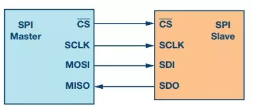
SDI (data input), SDO (data output), SCK (clock), CS (chip selection)
-
MISO: master input / slave output pin. This pin sends data in slave mode and receives data in master mode.
-
MOSI: master device output / slave device input pin. This pin sends data in master mode and receives data in slave mode.
-
SCLK: serial clock signal generated by the master equipment.
-
CS/SS: slave chip selection signal, controlled by master equipment. Its function is to be used as a "chip selection pin", that is, to select the specified slave device, so that the master device can communicate with the specific slave device separately to avoid conflicts on the data line.
1.SPI one to one:
2.SPI one to many:
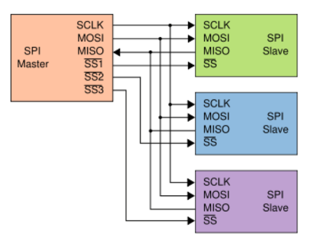
4. SPI device selection
SPI is a single master communication protocol, which means that only one central device in the bus can initiate communication.
When SPI master wants to read / write [slave]:
- It first pulls down the SS line corresponding to [slave] (SS is active at low level)
- Then start sending the working pulse to the clock line
- At the corresponding pulse time, [main equipment] sends the signal to MOSI to realize "write", and can sample MISO to realize "read"
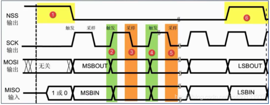
As shown below:
5. SPI data sending and receiving
SPI master and slave have a serial shift register. The master initiates a transmission by writing a byte to its SPI serial register.
- First, pull down the corresponding SS signal line to communicate with the device
- The host sends SCLK clock signal to tell the slave to write data or read data
It should be noted here that the SCLK clock signal may be active at low level or active at high level, because SPI has four modes, which will be introduced below
-
The master writes the data to be transmitted to the transmission data buffer (Menory), and the buffer passes through the shift register (0 ~ 7). The serial shift register moves the bytes bit by bit to the slave through the MOSI signal line. At the same time, the data received by the MISO interface is moved bit by bit to the reception buffer through the shift register
-
**Slave * * also returns the contents of its own serial shift register (0 ~ 7) to the host through MISO signal line. At the same time, it receives the data sent by the host through the MOSI signal line
In this way, the contents of the two shift registers are exchanged.
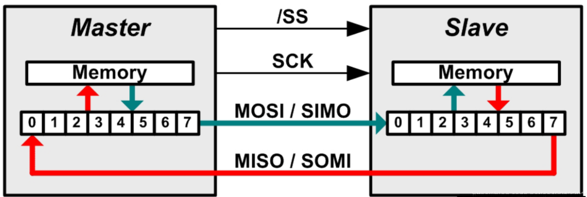
SPI can only be divided into master mode and slave mode. There is no saying of read and write. Write and read operations of peripherals are completed synchronously.
If only write operation is performed, the host only needs to ignore the received bytes; Conversely, if the master wants to read a byte from the slave, it must send an empty byte to trigger the transmission of the slave.
In other words, sending a data is bound to receive a data; To receive a data, you must also send a data first.
6. Four modes of SPI communication
The four modes of SPI are simply to set the signal of SCLK clock signal line as effective signal
The difference between them is that it defines which edge of the clock pulse converts the output signal, which edge samples the input signal, and the stable level value of the clock pulse (that is, whether it is high or low when the clock signal is invalid). Each mode is characterized by a pair of parameters, which are called clock polarity CPOL and clock phase CPHA.
- SPI communication has four different operation modes. Different slave devices may be configured to a certain mode at the factory, which cannot be changed
- But both sides of the first mock exam must work in the same mode.
- Therefore, we can configure the SPI mode of our master device and control the communication mode of our master device through CPOL (clock polarity) and CPHA (clock phase)
The details are as follows:
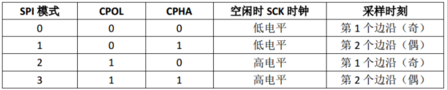
1. Clock polarity (CPOL) defines the idle state level of the clock:
CPOL=0 means that SCLK is in idle state when SCLK=0, so the effective state is that SCLK is in high level * * (high effective)**
CPOL=1 means that SCLK is in idle state when SCLK=1, so the effective state is that SCLK is at low level * * (low effective)**
2. The clock phase (CPHA) defines the data acquisition time.
CPHA=0, data sampling is performed at the first jump edge (rising edge or falling edge) of the clock. Send data at the second edge * * (1 acquisition and 2 transmission)**
CPHA=1, data sampling is performed at the second jump edge (rising edge or falling edge) of the clock. Send data at the first edge * * (1 engine and 2 acquisition)**
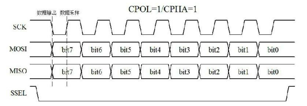
For example:
-
Mode0: CPOL=0, CPHA=0: when this space-time is idle, SCLK is at low level; Data sampling is at the first edge, that is, the jump of SCLK from low level to high level; Therefore, data sampling is on the rising edge and data transmission is on the falling edge.
-
Mode1: CPOL=0, CPHA=1: when this space-time is idle, SCLK is at low level; Data transmission is at the first edge, that is, the jump of SCLK from low level to high level; Therefore, data sampling is on the falling edge and data transmission is on the rising edge.
-
Mode2: CPOL=1, CPHA=0: when the space-time is idle, SCLK is at high level; Data sampling is at the first edge, that is, the jump of SCLK from high level to low level; Therefore, data acquisition is on the falling edge and data transmission is on the rising edge.
-
Mode3: CPOL=1, CPHA=1: when the space-time is idle, SCLK is at high level; Data transmission is at the first edge, that is, the jump of SCLK from high level to low level; Therefore, data acquisition is on the rising edge and data transmission is on the falling edge.
Note: data sampling = data preparation
CPOL=0: highly effective, 0 to 1, that is, the rising edge is the first edge
CPOL=1: low effective, 1 to 0, that is, the falling edge is the first edge
A table is:
Sequence diagram of four modes:
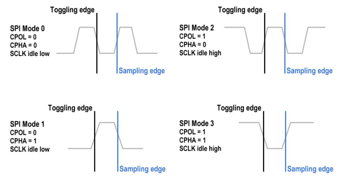
Note: Toggling edge = switching (sending) edge, Sampling edge = Sampling edge
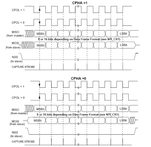
**Own thoughts: * * take SPI MODE 1 as an example, CPOL=0, CPHA=1, that is, high efficiency, 1 engine and 2 acquisition, that is, the first edge (i.e. rising edge) after low level sends data
It is more clear by referring to the following figure:
7. SPI communication protocol
The master and slave devices must use the same working mode - SCLK, CPOL and CPHA in order to work normally.
If there are multiple slave devices and they use different working modes, the master device must modify the mode of the corresponding slave device when reading and writing different slave devices.
SPI is like this. It does not specify the maximum transmission rate, address scheme, communication response mechanism and flow control rules.
As long as the four signal lines are connected correctly and the SPI mode is the same, pull the CS/SS signal line low, that is, direct communication can be realized, one byte at a time, and the data can be read and written at the same time. This is SPI
SPI does not care about the electrical characteristics of the physical interface, such as the standard voltage of the signal.
This is also a disadvantage of SPI interface: there is no specified flow control and no response mechanism to confirm whether data is received.
8. Three modes of SPI
SPI works in three modes: run, wait and stop.
1. Run Mode
This is the basic mode of operation
2. Wait Mode
SPI works in wait mode, which is a configurable low-power mode and can be controlled through the SPISWAI bit of SPICR2 register. In the wait mode, if the spiwai bit is cleared to 0, the SPI operation is similar to the operation mode. If the SPISWAI is in position 1, the SPI enters a low power state and the SPI clock will turn off. If SPI is configured as the host, all transfers will stop, but will restart after the CPU enters operation mode. If the SPI is configured as a slave, it will continue to receive and transmit a byte, so as to ensure that the slave is synchronized with the host.
3. Stop Mode
To reduce power consumption, SPI is inactive in stop mode. If the SPI is configured as a host, the ongoing transfer stops, but restarts after the CPU enters run mode. If the SPI is configured as a slave, it will continue to accept and send a byte, which ensures that the slave is synchronized with the host.
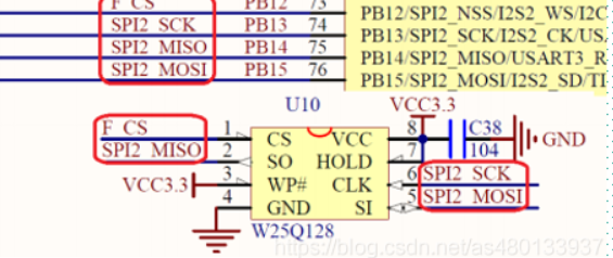
9. Schematic diagram
10. Code implementation process
SPI initialization configuration in STM32
- Initialize the GPIO port, configure the multiplexing function of relevant pins, and enable the SPIx clock. Calling function: void GPIO_Init();
- Enable SPI clock bus: RCC_APB2PeriphClockCmd(RCC_APB2Periph_SPI1,ENABLE)
- Configure SPI initialization parameters and set SPI working mode: SPI_ Init(SPI1,&SPI_Initstructure)
- Enable SPI peripherals: SPI_Cmd(SPI1,ENABLE);
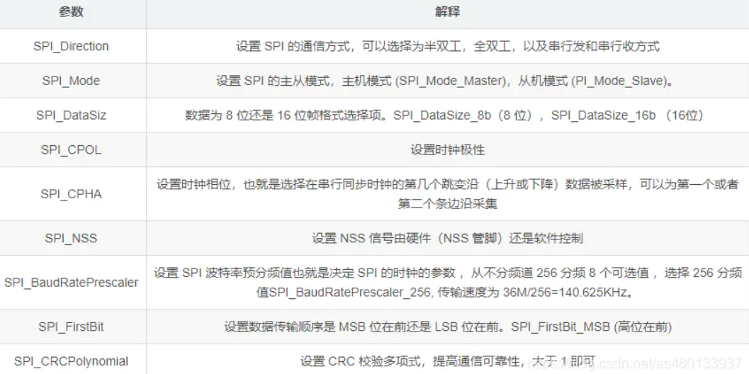
SPI configuration settings
typedef struct
{
uint16_t SPI_Direction; /*!< Transmission direction, two-way full duplex, one-way reception, etc*/
uint16_t SPI_Mode; /*!< Mode selection to determine whether the master or slave */
uint16_t SPI_DataSize; /*!< Data size, 8-bit or 16 bit */
uint16_t SPI_CPOL; /*!< Clock polarity selection */
uint16_t SPI_CPHA; /*!< Clock phase selection */
uint16_t SPI_NSS; /*!< Is the selection hardware or software*/
uint16_t SPI_BaudRatePrescaler; /*!< division factor  */
uint16_t SPI_FirstBit; /*!< Specifies whether the data transfer starts from the MSB or LSB bit. M
SB It is the first bit of binary and LSB is the last bit */
uint16_t SPI_CRCPolynomial; /*!< CRC Check, set CRC check polynomial to improve pass through
 Reliability, greater than 1*/
}SPI_InitTypeDef;
void SPI2_Init(void)
{
 	GPIO_InitTypeDef GPIO_InitStructure;
  SPI_InitTypeDef  SPI_InitStructure;

	RCC_APB2PeriphClockCmd(	RCC_APB2Periph_GPIOB, ENABLE );//PORTB clock enable
	RCC_APB1PeriphClockCmd(	RCC_APB1Periph_SPI2,  ENABLE );//SPI2 clock enable

	GPIO_InitStructure.GPIO_Pin = GPIO_Pin_13 | GPIO_Pin_14 | GPIO_Pin_15;
	GPIO_InitStructure.GPIO_Mode = GPIO_Mode_AF_PP;  //PB13/14/15 multiplex push-pull output
	GPIO_InitStructure.GPIO_Speed = GPIO_Speed_50MHz;
	GPIO_Init(GPIOB, &GPIO_InitStructure);//Initialize GPIOB

 	GPIO_SetBits(GPIOB,GPIO_Pin_13|GPIO_Pin_14|GPIO_Pin_15);  //PB13/14/15 pull-up

	SPI_InitStructure.SPI_Direction = SPI_Direction_2Lines_FullDuplex;  //Set SPI one-way or two-way data mode: SPI is set to two-wire two-way full duplex
	SPI_InitStructure.SPI_Mode = SPI_Mode_Master;		//Set SPI working mode: set as main SPI
	SPI_InitStructure.SPI_DataSize = SPI_DataSize_8b;		//Set SPI data size: SPI send receive 8-bit frame structure
	SPI_InitStructure.SPI_CPOL = SPI_CPOL_High;		//The idle state of the serial synchronization clock is high
	SPI_InitStructure.SPI_CPHA = SPI_CPHA_2Edge;	//The data of the second jump edge (rising or falling) of the serial synchronization clock is sampled
	SPI_InitStructure.SPI_NSS = SPI_NSS_Soft;		//Whether the NSS signal is managed by hardware (NSS pin) or software (using SSI bit): the internal NSS signal is controlled by SSI bit
	SPI_InitStructure.SPI_BaudRatePrescaler = SPI_BaudRatePrescaler_256;		//Define the baud rate prescaled value: the baud rate prescaled value is 256
	SPI_InitStructure.SPI_FirstBit = SPI_FirstBit_MSB;	//Specify whether data transmission starts from MSB bit or LSB bit: data transmission starts from MSB bit
	SPI_InitStructure.SPI_CRCPolynomial = 7;	//Polynomial for CRC value calculation
	SPI_Init(SPI2, &SPI_InitStructure);  //According to SPI_ Initializes the peripheral SPIx register with the parameters specified in initstruct

	SPI_Cmd(SPI2, ENABLE); //Enable SPI peripherals

	SPI2_ReadWriteByte(0xff);//Start transmission

}
SPI sending function (standard library / HAL Library)
u8 SPIx_ReadWriteByte(u8 TxData)
{
    u8 retry=0;
    while (SPI_I2S_GetFlagStatus(SPI2, SPI_I2S_FLAG_TXE) == RESET)
    {
    }//The waiting area is empty
    SPI_I2S_SendData(SPI2, TxData); //Send a byte data through the peripheral SPIx
    while (SPI_I2S_GetFlagStatus(SPI2, SPI_I2S_FLAG_RXNE) == RESET)
    {
    } //Wait for a byte to be received
    return SPI_I2S_ReceiveData(SPI2); //Returns the most recently received data through SPIx
}

HLA Library:
uint8_t SPI_SendByte(uint8_t byte)
{
    uint8_t d_read,d_send=byte;
    if(HAL_SPI_TransmitReceive(&hspi1,&d_send,&d_read,1,0xFFFFFF)!=HAL_OK)
    d_read=0XFF;
    return d_read;
Reference source of this study note:
https://blog.csdn.net/as480133937/article/details/105764119