1, nRF24L01 + module introduction
nRF24L01 + is a single-chip 2.4GHz transceiver suitable for ultra-low power wireless applications. NRF24L01 + is designed to operate in the global ISM band of 2.400-2.4835GHz.
to design a radio system using nRF24L01 +, only a single chip microcomputer (microcontroller) and some external passive components are required.
nRF24L01 + can be operated and configured through serial peripheral interface (SPI). The register diagram contains all configuration registers in nRF24L01 +, which can be accessed through SPI and in all operation modes of the chip.
nRF24L01 + is online compatible with nRF24L01, nRF2401A, nRF2402, nRF24E1 and nRF24E2. Compared with nRF24L01 +, the intermodulation and broadband blocking values in nRF24L01 + have been greatly improved. Adding internal filtering to nRF24L01 + improves the margin to meet the RF regulation standard.
1. Operating voltage requirements
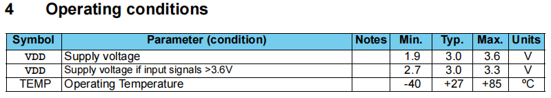
3.3V power supply is enough.
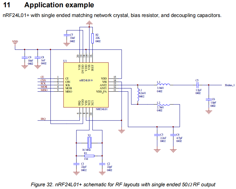
2. Module pin definition and schematic diagram
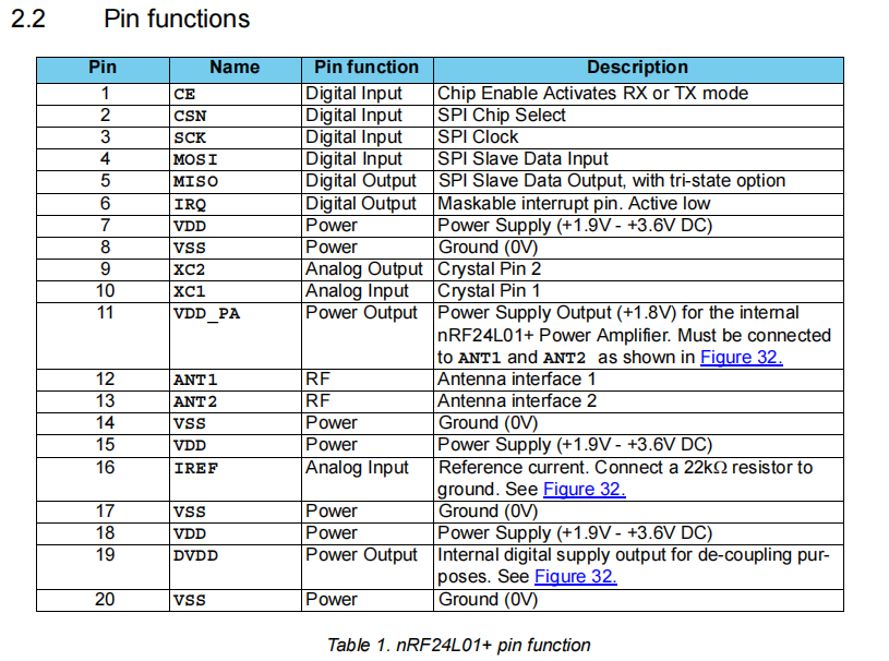
it is connected with MCU as a 4-wire SPI interface. In addition, CE output port and IRQ interrupt input port are required.
2, Register configuration
1. Description of working mode
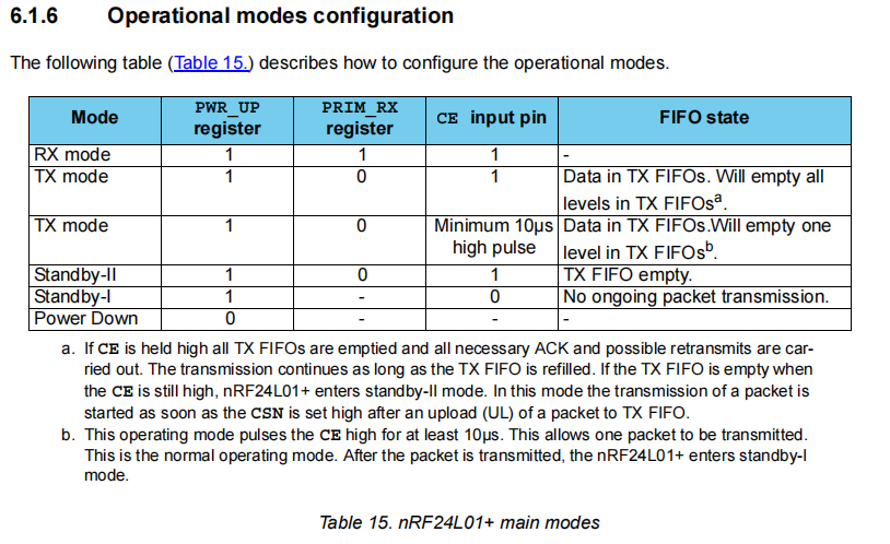
RX mode: the module receiving data is configured to this mode.
TX mode: the module that sends data is configured to this mode. Data is stored in TX FIFO register.
a. if the CE remains high, clear all TX FIFOs and perform all necessary confirmations and possible retransmissions. As long as the TX FIFO is refilled, the transmission will continue. If CE is still at high level when TX FIFO is empty, nRF24L01 + enters standby-II mode. In this mode, after uploading the data packet (UL) to TX FIFO, once the CSN is set to high, the transmission of the data packet begins.
b. in this working mode, CE high pulse lasts for at least 10 µ s. This will transmit a packet. This is the normal operating mode. After data packet transmission, nRF24L01 + enters standby mode-I mode.
Power Down mode: PWR_UP bit register write 0
2. Register command and address
the length in the Data Sheet is too long (p51 & p57-p63), so it is directly put into the definition in the program.
among them, the command required to configure the working mode: write the configuration register and add the register address CONFIG. Each bit of this register is defined as:
Only 7 bits can be written
Bit 6-4: interrupt enable setting
3 bits: CRC check enable
2 bits: 1or2 byte CRC
Bit 1: power supply
Bit 0: RX/TX control
according to the working mode configuration diagram, pay attention to the configuration of bits 1 and 0, and add the level of CE pin to configure the working mode.
ep: configure the module to receive RX mode
NRF24L01_Write_Reg(nRF_WRITE_REG + CONFIG, 0x0f); //Configure parameters of basic working mode; PWR_UP,EN_CRC,16BIT_CRC, receive mode, turn on all interrupts
refer to Data Sheet for other register configuration, and the form is the same as above.
3. Sending process
after the module is configured as the transmission mode, write the data into the transmission array and directly start the transmission function. The transmission function reads the interrupt flag TX after transmission_ After DS, clear the interrupt flag for next transmission.
4. Receiving process
after the module is configured as the receiving mode, when receiving a frame of data sent by other modules, RX of the STATUS register_ The Dr bit is set to 1 and an interrupt is triggered, which is fed back to the IRQ pin. After reading the data, you need to clear the interrupt flag and clear RX_FIFO register, otherwise the next reception cannot be carried out.
3, nRF24L01 module configuration code
the MCU model is STM32F103REx, the library is HAL library, and the operating system is rt-thread-2.0.0_ In the beta version, note that the initialization method of this program pin is different.
Header file 24L01 h
/**
	********************************************************************
	*	@file			24L01.h
	*	@version
	*	@date
	*	@brief
	********************************************************************
	*	@attention
	********************************************************************
	*/
#ifndef _24L01_H_
#define _24L01_H_

#include <stm32xxxx.h>
//#include <rtthread.h>

/**********  RF Passage***********/
#define NRF24L01_Channel 	0

/**********  NRF24L01 Register operation command***********/
#define nRF_ READ_ Reg 0x00 / / read the configuration register. The lower 5 bits are the register address
#define nRF_ WRITE_ Reg 0x20 / / write the configuration register. The lower 5 bits are the register address
#define RD_ RX_ Pload 0x61 / / read RX valid data, 1 ~ 32 bytes
#define WR_ TX_ Pload 0xa0 / / write TX valid data, 1 ~ 32 bytes
#define FLUSH_ TX 0xe1 / / clear TX FIFO register Used in sending mode
#define FLUSH_ RX 0xe2 / / clear RX FIFO register Used in receive mode
#define REUSE_ TX_ PL 0xe3 / / reuse the previous packet. CE is high and the packet is sent continuously
#Define NOP 0xff / / null operation. It can be used to read the status register
/**********  NRF24L01 Register address*************/
#Define config 0x00 / / configure register address
#define EN_ AA 0x01 / / enable auto answer function
#define EN_ Rxaddr 0x02 / / receive address allowed
#define SETUP_ Aw 0x03 / / set address width (all data channels)
#define SETUP_ Retr 0x04 / / create automatic retransmission
#define RF_ Ch 0x05 / / RF channel
#define RF_ Setup 0x06 / / RF register
#Define status 0x07 / / status register
#define OBSERVE_ TX 0x08 / / send detection register
#Define RPD 0x09 / / carrier detection register
#define RX_ ADDR_ P0 0x0a / / receiving address of data channel 0
#define RX_ ADDR_ P1 0x0b / / receive address of data channel 1
#define RX_ ADDR_ P2 0x0c / / receive address of data channel 2
#define RX_ ADDR_ P3 0x0D / / receive address of data channel 3
#define RX_ ADDR_ P4 0x0e / / data channel 4 receiving address
#define RX_ ADDR_ P5 0x0f / / receive address of data channel 5
#define TX_ Addr 0x10 / / send address register
#define RX_ PW_ P0 0X11 / / effective data width of receive data channel 0 (1 ~ 32 bytes)
#define RX_ PW_ P1 0x12 / / effective data width of receive data channel 1 (1 ~ 32 bytes)
#define RX_ PW_ P2 0x13 / / effective data width of receive data channel 2 (1 ~ 32 bytes)
#define RX_ PW_ P3 0x14 / / effective data width of receive data channel 3 (1 ~ 32 bytes)
#define RX_ PW_ P4 0x15 / / effective data width of receive data channel 4 (1 ~ 32 bytes)
#define RX_ PW_ P5 0x16 / / effective data width of receive data channel 5 (1 ~ 32 bytes)
#define FIFO_ Status 0x17 / / FIFO status register
/*-------------------------*/

/******  STATUS Register interrupt bit definition*******/
#define MAX_TX   	 0x10   	  // The maximum number of sending interrupts has been reached
#define TX_OK    	 0x20   	  // TX transmission completion interrupt
#define RX_OK    	 0x40   	  // Data interrupt received
/*-------------------------*/

/*********  24L01 Definition of sending and receiving data width 	  ***********/
#define TX_ ADR_ Width 5 / / 5 byte address width
#define RX_ ADR_ Width 5 / / 5 byte address width
#define TX_ PLOAD_ Width 32 / / 32 bytes effective data width
#define RX_ PLOAD_ Width 32 / / 32 bytes effective data width

/* NRF24L01 Port definition */
#define NRF24L01_PWR_gpio        C
#define NRF24L01_PWR_pin         10
#define NRF24L01_PWR_gpio_mode   Out_PP
#define NRF24L01_PWR			 PCout(NRF24L01_PWR_pin)
#define NRF24L01_IRQ_gpio        A
#define NRF24L01_IRQ_pin         8
#define NRF24L01_IRQ_gpio_mode   IPU
#define NRF24L01_IRQ   			 PAin(NRF24L01_IRQ_pin)

#define NRF24L01_CE_gpio         B
#define NRF24L01_CE_pin          11
#define NRF24L01_CE_gpio_mode    Out_PP
#define NRF24L01_CE   			 PBout(NRF24L01_CE_pin)

#define NRF24L01_CSN_gpio        B
#define NRF24L01_CSN_pin         12
#define NRF24L01_CSN_gpio_mode   Out_PP
#define NRF24L01_CSN   			 PBout(NRF24L01_CSN_pin)

#define NRF24L01_SCK_gpio        B
#define NRF24L01_SCK_pin         13
#define NRF24L01_SCK_gpio_mode   Out_PP
#define NRF24L01_SCK   			 PBout(NRF24L01_SCK_pin)

#define NRF24L01_MISO_gpio       B
#define NRF24L01_MISO_pin        14
#define NRF24L01_MISO_gpio_mode  IPU
#define NRF24L01_MISO  			 PBin(NRF24L01_MISO_pin)

#define NRF24L01_MOSI_gpio       B
#define NRF24L01_MOSI_pin        15
#define NRF24L01_MOSI_gpio_mode  Out_PP
#define NRF24L01_MOSI  			 PBout(NRF24L01_MOSI_pin)

/* variable */
u8 TX_ADDRESS[TX_ADR_WIDTH] = {0xFF, 0xFF, 0xFF, 0xFF, 0xFF}; //Sending address
u8 RX_ADDRESS[RX_ADR_WIDTH] = {0xFF, 0xFF, 0xFF, 0xFF, 0xFF}; //Receiving address
u8 NRF24L01_Recv_buf[32];//The first byte is the packet length and does not contain the first byte
u8 NRF24L01_Send_buf[32];

/* function */
u8   SPI_RW(u8  byte);
u8   NRF24L01_Write_Reg(u8  reg, u8  value);
u8   NRF24L01_Read_Reg(u8  reg);
u8   NRF24L01_Read_Buf(u8  reg, u8  *pBuf, u8  len);
u8   NRF24L01_Write_Buf(u8  reg, u8  *pBuf, u8  len);
u8   NRF24L01_RxPacket(u8  *rxbuf);
u8   NRF24L01_TxPacket(u8  *txbuf);
u8   NRF24L01_Check(void);
void NRF24L01_RT_Init(void);
void NRF24L01_SEND_BUF(u8 *buf);
void NRF24L01_Init(void);
void NRF24L01_Receive(void);
void NRF24L01_Send_online(void);

#endif
Source file 24L01 c
#include "24L01.h"
#include "gpio.h"
#include "flash.h"
#include "delay.h"
#include "24L01_app.h"

/**
	*	@name		  SPI_RW
	*	@brief		Send the register address and read the status value
	*	@param		byte 1byte data to be sent
	*	@retval		Received data returned from slave
	*/
u8 SPI_RW(u8 byte)
{
    u8 bit_ctr;
    for(bit_ctr = 0; bit_ctr < 8; bit_ctr++) // Output 8 bits
    {
        if((u8)(byte & 0x80) == 0x80)
        {
            NRF24L01_MOSI = 1;    // MSB TO MOSI
        }
        else
        {
            NRF24L01_MOSI = 0;
        }
        byte = (byte << 1);					 // shift next bit to MSB
        NRF24L01_SCK = 1;
        byte |= NRF24L01_MISO;	     // capture current MISO bit
        NRF24L01_SCK = 0;
    }
    return byte;
}

/*********************************************/
/* Function function: write value to 24L01 register (one byte) */
/* Entry parameter: reg register address to be written          */
/*           value Write value to register            */
/* Exit parameter: status value                   */
/*********************************************/
u8 NRF24L01_Write_Reg(u8 reg, u8 value)
{
    u8 status;
    NRF24L01_CE = 0;
	NRF24L01_CSN = 0;                //CSN=0, select slave and start sending
    status = SPI_RW(reg);		//Send the register address and read the status value
    SPI_RW(value);
    NRF24L01_CSN = 1;                //CSN=1;
    return status;
}

/*************************************************/
/* Function: read the register value of 24L01 (one byte)      */
/* Entry parameter: reg register address to be read               */
/* Exit parameter: value reads the value of the register                */
/*************************************************/
u8 NRF24L01_Read_Reg(u8 reg)
{
    u8 value;
    NRF24L01_CSN = 0;            //CSN=0;
    SPI_RW(reg);			//Send the register value (position) and read the status value
    value = SPI_RW(NOP);
    NRF24L01_CSN = 1;            //CSN=1;
    return value;
}

/*********************************************/
/* Function function: read the register value of 24L01 (multiple bytes)   */
/* Entry parameter: reg register address                */
/*           *pBuf Storage array for reading register values    */
/*           len   Array byte length              */
/* Exit parameter: status value                   */
/*********************************************/
u8 NRF24L01_Read_Buf(u8 reg, u8 *pBuf, u8 len)
{
    u8 status, u8_ctr;
    NRF24L01_CSN = 0;                   			//CSN=0
    status = SPI_RW(reg);					//Send the register address and read the status value
    for(u8_ctr = 0; u8_ctr < len; u8_ctr++)
    {
        pBuf[u8_ctr] = SPI_RW(NOP);    //Read data
    }
    NRF24L01_CSN = 1;                 			//CSN=1
    return status;        					//Returns the read status value
}

/**********************************************/
/* Function function: write value to 24L01 register (multiple bytes)  */
/* Entry parameter: reg register address to be written            */
/*           *pBuf Storage array of values               */
/*           len   Array byte length               */
/**********************************************/
u8 NRF24L01_Write_Buf(u8 reg, u8 *pBuf, u8 len)
{
    u8 status, u8_ctr;
    NRF24L01_CSN = 0;
    status = SPI_RW(reg);					//Send the register value (position) and read the status value
    for(u8_ctr = 0; u8_ctr < len; u8_ctr++)
    {
        SPI_RW(*pBuf++);    //Write data
    }
    NRF24L01_CSN = 1;
    return status;          				//Returns the read status value
}

/*********************************************/
/* Function: 24L01 receives a packet             */
/* Entry parameter: rxbuf receive data array              */
/* Return value: 0 successfully received data                 */
/*          1   No data received                 */
/*********************************************/
u8 NRF24L01_RxPacket(u8 *rxbuf)
{
    u8 state;
    state = NRF24L01_Read_Reg(nRF_READ_REG + STATUS);  			//Read the value of the status register
    NRF24L01_Write_Reg(nRF_WRITE_REG + STATUS, state);  		//Clear TX_DS or MAX_RT interrupt flag
    if(state & RX_OK)											//Data received
    {
        NRF24L01_CE = 0;
        NRF24L01_Read_Buf(RD_RX_PLOAD, rxbuf, RX_PLOAD_WIDTH); 	//Read data
        NRF24L01_Write_Reg(FLUSH_RX, 0xff);						//Clear RX FIFO register
        NRF24L01_CE = 1;
        rt_thread_delay(1);
        return 0;
    }
    return 1;//No data received
}

/**********************************************/
/* Function function: 24L01 sends a packet              */
/* Entry parameter: txbuf send data array              */
/* Return value; 0x10 maximum number of retransmissions reached, sending failed*/
/*          0x20    Successful sending completed              */
/*          0xff    fail in send                  */
/**********************************************/
u8 NRF24L01_TxPacket(u8 *txbuf)
{
    u8 state;
    NRF24L01_CE = 0;											//CE is pulled down to enable 24L01 configuration
    NRF24L01_Write_Buf(WR_TX_PLOAD, txbuf, TX_PLOAD_WIDTH);		//Write data to TX buf 32 bytes
    NRF24L01_CE = 1;											//CE is set high to enable transmission
    while(NRF24L01_IRQ == 1);									//Wait for sending to complete
    state = NRF24L01_Read_Reg(nRF_READ_REG + STATUS);  			//Read the value of the status register
    NRF24L01_Write_Reg(nRF_WRITE_REG + STATUS, state); 			//Clear TX_DS or MAX_RT interrupt flag
    if(state & MAX_TX)											//Maximum number of retransmissions reached
    {
        NRF24L01_Write_Reg(FLUSH_TX, 0xff);						//Clear TX FIFO register
        return MAX_TX; //Pairing failure return value
    }
    if(state & TX_OK)											//Send complete
    {
        NRF->pair_ACK = 1;
        return TX_OK; //Return value of pairing success
    }
    return 0xff;												//fail in send
}

/********************************************/
/* Function: check whether 24L01 exists              */
/* Return value; 0 exists                        */
/*           1  non-existent                      */
/********************************************/
u8 NRF24L01_Check(void)
{
    u8 check_in_buf[5] = {0x11, 0x22, 0x33, 0x44, 0x55};
    u8 check_out_buf[5] = {0x00};
    NRF24L01_SCK = 0;
    NRF24L01_CSN = 1;
    NRF24L01_CE = 0;
    NRF24L01_Write_Buf(nRF_WRITE_REG + TX_ADDR, check_in_buf, 5);
    NRF24L01_Read_Buf(nRF_READ_REG + TX_ADDR, check_out_buf, 5);
    if((check_out_buf[0] == 0x11) && \
            (check_out_buf[1] == 0x22) && \
            (check_out_buf[2] == 0x33) && \
            (check_out_buf[3] == 0x44) && \
            (check_out_buf[4] == 0x55)) { return 0; }
    else { return 1; }
}

/**
	*	@name		NRF24L01_RT_Init
	*	@brief
	*	@param		None
	*	@retval		None
	*/
void NRF24L01_RT_Init(void)
{
	NRF24L01_CE = 0;
	NRF24L01_Write_Reg(nRF_WRITE_REG + CONFIG, 0x0f); 								//Configure parameters of basic working mode; PWR_UP,EN_CRC,16BIT_CRC, receive mode, turn on all interrupts
	NRF24L01_Write_Reg(nRF_WRITE_REG + EN_AA, 0x01);  								//Enable auto reply for channel 0
	NRF24L01_Write_Reg(nRF_WRITE_REG + EN_RXADDR, 0x01); 							//Enable the receive address of channel 0
	NRF24L01_Write_Reg(nRF_WRITE_REG + SETUP_RETR, 0x1a); 							//Set automatic retransmission interval: 500us + 86us; Maximum number of automatic retransmissions: 10
	NRF24L01_Write_Reg(nRF_WRITE_REG + RF_CH, NRF24L01_Channel);   					//Set RF channel to CHANAL
	NRF24L01_Write_Reg(nRF_WRITE_REG + RF_SETUP, 0x0f); 							//Set TX transmission parameters, 2Mbps,0db gain, low noise gain on
	NRF24L01_Write_Buf(nRF_WRITE_REG + RX_ADDR_P0, (u8*)RX_ADDRESS, RX_ADR_WIDTH);	//Setting the TX node address is mainly to enable ACK
	NRF24L01_Write_Buf(nRF_WRITE_REG + TX_ADDR, (u8*)TX_ADDRESS, TX_ADR_WIDTH); 	//Write TX node address
	NRF24L01_Write_Reg(nRF_WRITE_REG + RX_PW_P0, RX_PLOAD_WIDTH); 					//Select a valid data width for channel 0
	NRF24L01_Write_Reg(FLUSH_RX, 0xff);												//Clear RX FIFO register
	NRF24L01_CE = 1; 																//CE is set high to enable transmission
}

/**
	*	@name		NRF24L01_SEND_BUF
	*	@brief	2.4G send data
	*	@param	buf: array
	*	@retval	NONE
	*/
void NRF24L01_SEND_BUF(u8 *buf)
{
	NRF24L01_CE = 0;
	NRF24L01_Write_Reg(nRF_WRITE_REG + CONFIG, 0x0e);	//Launch mode
	NRF24L01_CE = 1;
	rt_thread_delay(1);
	NRF24L01_TxPacket(buf);	//Send a packet
	NRF24L01_CE = 0;
	NRF24L01_Write_Reg(nRF_WRITE_REG + CONFIG, 0x0f);	//Receiving mode
	NRF24L01_CE = 1;
}

/**
	*	@name		NVIC_Configuration_24l01 Interrupt initialization
	*	@brief
	*	@param		None
	*	@retval		None
	*/
static void NVIC_Configuration_24l01(void)
{
    NVIC_InitTypeDef NVIC_InitStructure;

#ifdef  VECT_TAB_RAM
    /* Set the Vector Table base location at 0x20000000 */
    NVIC_SetVectorTable(NVIC_VectTab_RAM, 0x0);
#else  /* VECT_TAB_FLASH  */
    /* Set the Vector Table base location at 0x08000000 */
    NVIC_SetVectorTable(NVIC_VectTab_FLASH, 0x0);
#endif

    /* Configure one bit for preemption priority */
    NVIC_PriorityGroupConfig(NVIC_PriorityGroup_1);
    /* Enable the EXTI0 Interrupt */
    NVIC_InitStructure.NVIC_IRQChannel = EXTI0_IRQn;
    NVIC_InitStructure.NVIC_IRQChannelPreemptionPriority = 0;
    NVIC_InitStructure.NVIC_IRQChannelSubPriority = 0;
    NVIC_InitStructure.NVIC_IRQChannelCmd = ENABLE;
    NVIC_Init(&NVIC_InitStructure);
}

/**
	*	@name		SPI_GPIO_Init
	*	@brief		24l01 Port initialization
	*	@param		None
	*	@retval		None
	*/
static void SPI_GPIO_Init(void)
{
	GPIO_Pin_Setup(NRF24L01_PWR_gpio,  NRF24L01_PWR_pin,  NRF24L01_PWR_gpio_mode);	//Power supply pin
	GPIO_Pin_Setup(NRF24L01_IRQ_gpio,  NRF24L01_IRQ_pin,  NRF24L01_IRQ_gpio_mode);	//Interrupt pin
    GPIO_Pin_Setup(NRF24L01_CE_gpio,   NRF24L01_CE_pin,   NRF24L01_CE_gpio_mode);	//Mode selection pin
    GPIO_Pin_Setup(NRF24L01_CSN_gpio,  NRF24L01_CSN_pin,  NRF24L01_CSN_gpio_mode);	//Chip selection pin
    GPIO_Pin_Setup(NRF24L01_SCK_gpio,  NRF24L01_SCK_pin,  NRF24L01_SCK_gpio_mode);	//Clock signal pin
	GPIO_Pin_Setup(NRF24L01_MISO_gpio, NRF24L01_MISO_pin, NRF24L01_MISO_gpio_mode);	//Data input pin
    GPIO_Pin_Setup(NRF24L01_MOSI_gpio, NRF24L01_MOSI_pin, NRF24L01_MOSI_gpio_mode);	//Data output pin
	NVIC_Configuration_24l01();	//Interrupt configuration
}

/**
	*	@name		NRF24L01_Init
	*	@brief		2.4G initialization
	*	@param		None
	*	@retval		None
	*/
void NRF24L01_Init(void)
{
    SPI_GPIO_Init();
    NRF24L01_CE = 1;
    NRF24L01_CSN = 1;
    NRF24L01_SCK = 1;
    NRF24L01_MOSI = 1;
    NRF24L01_PWR(1);
    while(NRF24L01_Check())	//Wait until NRF24L01 is detected before the program is executed downward
    {
		rt_thread_delay(1);
    }
    NRF24L01_RT_Init();
}
the bottom driver is completed and configured to receive mode. Here and below are the receiving application codes. Address pairing is made, which is only for reference.
24L01_app.h
#define static_addr  	 0 				// Modify TX_ADDRESS_static
#define dynamic_addr  	 one 						// Dynamic address generated by CPUID
#define NRF24L01_pair_addr 	 dynamic_addr   	// 2.4G address mode

int NRF24l01_thread_create(u16 stack, u8 priority, u8 delay);
24L01_app.c. This part is the thread of rtthread
#include "sys.h"
#include "24L01.h"
#include "gpio.h"
#include "flash.h"
#include "delay.h"
#include "24L01_app.h"

u8 pair_flag_clear = 0;
u8 pair_flag = 0;
/**
	*	@name		NRF24l01_dynamic_thread_entry
	*	@brief	2.4G wireless communication
	*	@param	None
	*	@retval	None
	*/
static void NRF24l01_dynamic_thread_entry(void* parameter)
{
    u8 i;
    static u8 addrset_flash_wipe_once = 0;
    rt_lock(1);
    NRF24L01_Init();	//Module initialization
    NRF24L01_pairFlag_Read();
    NRF24L01_Addr_Init();	//Address initialization. The address part is to identify the data frames of different devices (customized)
    rt_lock(0);
    while (1)
    {
       /* NRF24L01 Data received by wireless module */
       if(NRF24L01_IRQ == 0)
       {
          if(NRF24L01_RxPacket(NRF24L01_Recv_buf) == 0)
          {
            if(....)
            {
              /*Here is the received data processing code*/
            }
            //Address pairing. The address part is to identify the data frames of different devices (customized)
            else if((NRF24L01_Recv_buf[1] == 0xAA) && (NRF24L01_Recv_buf[2] == 0xBB)) //Address pairing
            {
               pair_flag = 1;
               flashDataWrite[0] = 1;
               for(i = 0; i < 6; i++)
               {
                   flashDataWrite[i + 1] = NRF24L01_Recv_buf[i + 3];
               }
               //Write flash
               if(addrset_flash_wipe_once == 0)
               {
                  addrset_flash_wipe_once = 1;
#if NRF24L01_pair_addr == dynamic_addr
			      rt_lock(1);
			      Flash_Write(0, flashDataWrite, sizeof(flashDataWrite));
			      rt_lock(0);
			      softReset();
#endif
               }
            }
          }
       }
       else
       {
          /* Data action not received */
       }
       NRF24L01_addr_config();
       rt_thread_delay(10);
    }
}
/**
	*	@name		NRF24l01_thread_create
	*	@brief  Thread initialization
	*	@param	(stack, priority, delay)
	*	@retval	None
	*/
int NRF24l01_thread_create(u16 stack, u8 priority, u8 tick)
{
    rt_err_t result;
    /* Dynamic thread control block pointer */
    rt_thread_t NRF24l01_thread;
    /* Create dynamic thread */
    NRF24l01_thread = rt_thread_create("NRF24l01_thread",
                                       NRF24l01_dynamic_thread_entry, RT_NULL,
                                       stack, priority, tick);
    if (NRF24l01_thread != RT_NULL)
    {
        rt_thread_startup(NRF24l01_thread);
    }
    return 0;
}
/**
	*	@name		NRF24L01_Addr_Init
	*	@brief	NRF24l01 Address initialization
	*	@param	None
	*	@retval	None
	*/
void NRF24L01_Addr_Init(void)
{
    static u8 i;
/* Dynamic communication address */
#if NRF24L01_pair_addr == dynamic_addr
    /* If paired, use the pairing address */
    if(pair_flag == 1)
    {
        TX_ADDRESS[0] = flashDataRead[1];
        TX_ADDRESS[1] = flashDataRead[2];
        TX_ADDRESS[2] = flashDataRead[3];
        TX_ADDRESS[3] = flashDataRead[4];
        TX_ADDRESS[4] = flashDataRead[5];
    }
    else
    {
        TX_ADDRESS[0] = 0xFF;
        TX_ADDRESS[1] = 0xFF;
        TX_ADDRESS[2] = 0xFF;
        TX_ADDRESS[3] = 0xFF;
        TX_ADDRESS[4] = 0xFF;
    }

    for(i = 0; i < TX_ADR_WIDTH; i++)
    {
        RX_ADDRESS[i] = TX_ADDRESS[i];
    }
/**
	*	@name		NRF24L01_addr_config
	*	@brief		NRF24l01 address
	*	@param		None
	*	@retval		None
	*/
void NRF24L01_addr_config(void)
{
#if NRF24L01_pair_addr == dynamic_addr
    /* Press the extension key: NRF24L01 address restores the factory setting full FF */
    if(pair_flag_clear == 1)//pair_flag_clear is assigned by other threads
    {
        pair_flag == 0;
        pair_flag_clear = 0;
        rt_lock(1);
        flashDataWrite[0] = 0;
        Flash_Write(0, flashDataWrite, sizeof(flashDataWrite)); //Erase flash
        rt_lock(0);
        softReset();
    }
#endif
}
/*****************The following is the data frame style of custom address pairing*****************/
/**
	*	@name		NRF24L01_Send_dynamicCommunicationAddress
	*	@brief		NRF24L01 Send dynamic address
	*	@param		None
	*	@retval		None
	*/
void NRF24L01_Send_dynamicCommunicationAddress(void)
{
    DataLength = 0x08;
    NRF24L01_Send_buf[0] = DataLength;//Data length
    NRF24L01_Send_buf[1] = Target_Addr;//Destination address
    NRF24L01_Send_buf[2] = Source_Addr;//source address
    NRF24L01_Send_buf[3] = dynamicCommunicationAddress[0];
    NRF24L01_Send_buf[4] = dynamicCommunicationAddress[1];
    NRF24L01_Send_buf[5] = dynamicCommunicationAddress[2];
    NRF24L01_Send_buf[6] = dynamicCommunicationAddress[3];
    NRF24L01_Send_buf[7] = dynamicCommunicationAddress[4];
    if(pair_flag == 1)
    {
        NRF24L01_Send_buf[8] = 1;
    }
    else
    {
        NRF24L01_Send_buf[8] = 0;
    }
    NRF24L01_SEND_BUF(NRF24L01_Send_buf);
}
/**
	*	@name		Dynamic_Comm_Address
	*	@brief		According to Cpu_Id generate dynamic communication address
	*	@param		None
	*	@retval		None
	*/
u8 dynamicCommunicationAddress[5] = {0};
void Dynamic_Comm_Address(void)
{
    Cpu_Id_Get();
    dynamicCommunicationAddress[0] = (uint8_t)(Cpu_Id[0] & 0x000000FF);
    dynamicCommunicationAddress[1] = (uint8_t)(Cpu_Id[1] & 0x000000FF);
    dynamicCommunicationAddress[2] = (uint8_t)(Cpu_Id[2] & 0x000000FF);
    dynamicCommunicationAddress[3] = (uint8_t)(((Cpu_Id[0] & Cpu_Id[1]) & 0x000FF000) >> 12);
    dynamicCommunicationAddress[4] = (uint8_t)(((Cpu_Id[1] & Cpu_Id[2]) & 0x000FF000) >> 12);
}
/**
	*	@name		Cpu_Id_Get
	*	@brief		Get the id of cpu
	*	@param		None
	*	@retval		Success or failure
	*/
u32 Cpu_Id[3] = {0};
void Cpu_Id_Get(void)
{
    Cpu_Id[0] = *(__IO u32*)(0x1FFFF7E8);
    Cpu_Id[1] = *(__IO u32*)(0x1FFFF7EC);
    Cpu_Id[2] = *(__IO u32*)(0x1FFFF7F0);
}
/**
	*	@name		NRF24L01_pairFlag_Read
	*	@brief  Read the 2.4G address flag bit and execute it during initialization
	*	@param	None
	*	@retval	None
	*/
void NRF24L01_pairFlag_Read(void)
{
#if NRF24L01_pair_addr == dynamic_addr
    Flash_Read(0, flashDataRead, sizeof(flashDataRead));
    if(flashDataRead[0] == 1) //Read NRF24L01 pairing flag bit
    {
       pair_flag = 1;
    }
#endif
}
Header file flash h
#ifndef _flash_H_
#define _flash_H_

#include "stm32f10x_flash.h"

#Define startaddr 0x0807f800 / / top address of main memory page 255
//0x08007C00

/* variable */
extern  u8  flashDataWrite[6];
extern  u8  flashDataRead[6];

/* function */
void Flash_Write(u32 WriteAddr, u8 *DataToWrite, u8 WriteNum);
void Flash_Read(u32 ReadAddr, u8*DataToRead, u8 ReadNum);

#endif
Original file flash c
#include "flash.h"

/* variable */
volatile FLASH_Status FLASHStatus = FLASH_COMPLETE;
u8 flashDataWrite[6] = {0};//The first byte is the pairing flag bit, and the last five bytes are the address
u8 flashDataRead[6] = {0};
/**
*	@name		Flash_Write
*	@brief      Write data to internal flash
*	@param		WriteAddr: Write data address offset
*				DataToWrite: Data to write
*               num: Number of written data
*	@retval		None*/
void Flash_Write(uint32_t WriteAddr, uint8_t *DataToWrite, uint8_t WriteNum)
{
    uint32_t addr;
    uint8_t i;
    addr = (uint32_t)STARTADDR + WriteAddr;
    FLASH_Unlock();
    FLASH_ClearFlag(FLASH_FLAG_BSY | FLASH_FLAG_EOP | FLASH_FLAG_PGERR | FLASH_FLAG_WRPRTERR);
    FLASH_ErasePage(addr);
    for(i = 0; i < WriteNum; i++)
    {
        FLASH_ProgramWord(addr, DataToWrite[i]);
        addr += 4;
    }
    FLASH_ClearFlag(FLASH_FLAG_BSY | FLASH_FLAG_EOP | FLASH_FLAG_PGERR | FLASH_FLAG_WRPRTERR);
    FLASH_Lock();
}


/**
	*	@name		Flash_Read
	*	@brief      Read N bytes of the specified address of the internal flash
	*	@param		ReadAddr: Specify address
	*				DataToRead: Data store pointer
	*				ReadNum: Number of bytes read
	*	@retval		None
	*/
void Flash_Read(uint32_t ReadAddr, uint8_t *DataToRead, uint8_t ReadNum)
{
    uint8_t i;
    uint32_t addr;
    addr = (uint32_t)STARTADDR + ReadAddr;
    for(i = 0; i < ReadNum; i++)
    {
        DataToRead[i] = *(uint32_t*)(addr);
        addr += 4;
    }
}
summary
as the nRF24L01 module driver, only the underlying driver is applicable, and other parts of the code are used as a reference, which can be adopted and written according to their own needs.
the communication effect of this module is not very good, and domestic models SI24R1 and SI24L01 are mixed. Do not mix the transceiver module when using it, otherwise there will be inexplicable problems.