preface
This blog is based on your own needs and the needs of the interview position, so I specially come to learn the two common communication protocols SPI and IIC again. The development board used here is STM32F03_MIN
I also hope this blog can be of some help to you!
IIC protocol
I ² C. Usually read as "i-Party C", it is a serial communication bus with multi master-slave architecture. Designed by Philips in 1980, it is used to connect motherboard, embedded system or mobile phone to low-speed peripheral devices. Nowadays, it is a very common communication protocol in the embedded field. It is commonly used for MPU/MCU connection, communication and data transmission with external equipment.
IIC consists of two lines, one bidirectional serial data line SDA and one serial clock line SCL. Each device connected to the bus has an independent address through which the host can access different devices. Because IIC protocol is relatively simple, GPIO is often used to simulate IIC timing. This method is called analog IIC. If the IIC controller of MCU is used and the IIC controller is set, the IIC controller will automatically realize the protocol timing. This method is called hardware IIC. Because the speed of IIC equipment is relatively low, usually both methods can be used. Simulating IIC is convenient for transplantation, and the working efficiency of hardware IIC is relatively high.
As for the IIC protocol, I believe you can clearly understand it through the example of students' football passed by the teacher
 Regard teachers as MCU/MPU and students as peripheral equipment.
First, the teacher kicks the ball to a student, that is, the host sends data to the slave. The steps are as follows:
- Teacher: start;
- Teacher: A! I'll serve you! (address / direction);
- Student A: Yes! (response);
- The teacher sent the ball out (transmission);
- A should tell the teacher after receiving the ball;
- Teacher: end (stop);
When MCU sends data, it needs to get a response from the equipment. When the data transmission is completed, MCU automatically stops sending, and the equipment does not need to respond.
Then the teacher asked the students to pass the ball to themselves, that is, to send data from the machine to the host. The steps are as follows:
- Teacher: start;
- Teacher: B! Give me the ball! (address / direction);
- Student B: Yes!
- B send the ball to the teacher (transmission);
- After receiving the ball, the teacher said to B that he had received the ball (response);
- Teacher: end (stop).
When MCU receives the data transmitted by peripheral equipment, it first sends instructions to the equipment to send the signal of data. After receiving it, the equipment responds to MCU. At the same time, MCU also responds to peripheral equipment when it receives data. When the data transmission is completed, MCU automatically ends the transmission.
It can be seen from the above examples that the teacher (host) dominates the passing and follows the standard process (Communication Protocol) to ensure the accuracy of passing. The process of receiving and serving is summarized as follows:
① The teacher said start, indicating the start signal;
② The teacher reminds a student to serve, indicating the sending address and direction (address/read/write);
③ The student responds to the teacher (ack);
④ The teacher serves / receives the ball, indicating the transmission of data;
⑤ Response after receiving the ball: response signal (ACK);
⑥ When the teacher says "end", it means that the IIC transmission is over §.
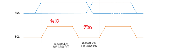
Data validity
IIC consists of two lines, one bidirectional serial data line SDA and one serial clock line SCL. The data on the SDA line must remain stable in the high-level cycle of the clock. The high-level or low-level state of the data line can be changed only when the clock signal of the SCL line is low. In other words, SCL indicates valid data at high level, SDA indicates "1" at high level and "0" at low level; SCL is a low level, indicating five valid data. At this time, SDA will switch the level to prepare for the next data representation. As shown below
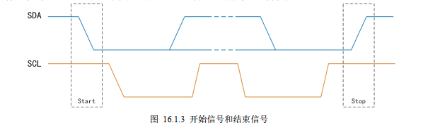
Start signal and end signal
IIC start signal (S): when SCL is high, SDA is converted from high level to low level;
IIC stop signal (P): when SCL is at high level, SDA is converted from low level to high level;
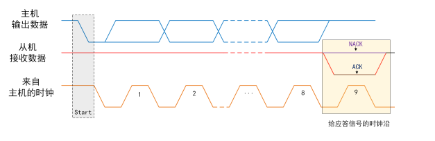
Response signal
IIC transmits 8-bit data each time. After each transmission, the slave needs to feed back a response bit to confirm whether the slave receives data normally. When the host sends 8-bit data, another clock will be generated. At this time, the host releases the control of SDA and reads the SDA level. Under the influence of pull-up resistance, SDA defaults to high and must be pulled down from the host to confirm the receipt of data.
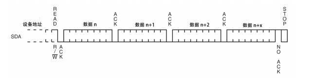
Complete transmission process
The complete transmission process of IIC is as follows:
- SDA and SCL are high at first, and then the host pulls SDA low, indicating the start signal;
- In the next eight time periods, the host controls the level of SDA and sends the slave address. If the 8th is 0, it means that the next is a write operation, that is, the host transmits it to the slave; If it is 1, it means that the next operation is read. That is, the slave transmits data to the host (determines the transmission direction); In addition, data transmission is from high to low, so the transmission mode is bit MSB
- The device corresponding to the slave address in the bus sends a response signal;
- In the next 8 time cycles, if it is a write operation, the host controls the level of SDA; If it is a read operation, the slave controls the height of SDA;
- Each time the transmission is completed, the equipment receiving data sends a response signal;
- Finally, when SCL is high, the host is pulled up from low and the whole transmission ends.
Introduction to EEPROM
The full name of EEPROM is "electrically erasable programmable read only register". It is usually used to store user configuration information data. For example, when the development board runs for the first time, it needs screen calibration, and the calibrated configuration signal can be saved in EEPROM. After the development board is powered off, it will not be lost. The next time it starts, the development board will automatically read the calibration configuration information of EEPROM, so there is no need to recalibrate.
The essence of EEPROM and flash is the same. Flash includes MCU internal flash and external extended flash. This development board has an external flash with SPI interface, which will be introduced later. Functionally, flash usually stores running code and will not be modified during operation, while EEPROM stores user data and may be modified repeatedly. Structurally, flash operates by sector and EEPROM usually operates by byte. The difference between the two will not be discussed too much here. Just understand the role of EEPROM in embedded system.
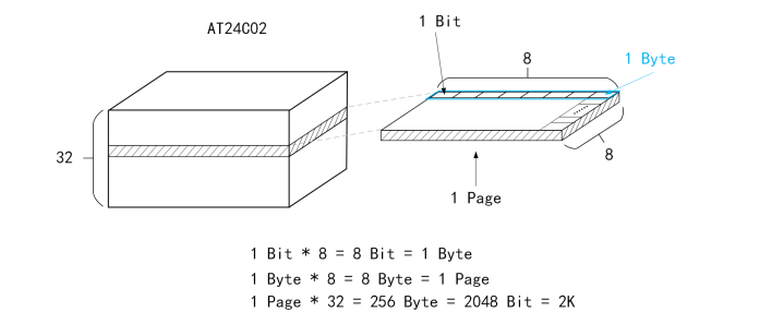
Structural composition
Device address
IIC devices will have a device address. For ATC2402 with different capacities, the definition of device address will be different. It can be seen from the data manual
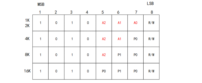
The capacity of AT24C02 is 2K, corresponding to the first line in the figure above. The high four bits are fixed as "1010". The middle three bits are determined by the level of A2, A1 and A0 pins. For example, if A2~0 pins are fully grounded, the value is "000". The last lowest bit is read-write bit, 0 represents write command and 1 represents read command. A2, A1 and A0 pin levels need to be determined by the schematic diagram. Assuming that the full power supply is grounded, if you need to write data to AT24C02, send the address "1010 0000". If you need to read data to AT24C02, send the address "1010 0001".
Suppose there are multiple AT24C02 hanging on the same I on the development board ² On the C bus, through this rule, it is only necessary to design the circuit and make the A2, A1 and A0 pin levels different to distinguish the two AT24C02.
For AT24Cxx series with larger capacity, such as AT24C04, the device address is determined by A2 and A1 pins, and the data space is determined by P0. For example, for the 02K space operation of AT24C04, P0 is 0, and for the 2K4K space operation, P0 is 1.
Write AT24Cxx
AT24Cxx supports byte write mode and page write mode. Byte write mode is the writing of one address and one data; The page write mode is to write data continuously. Multiple data at one address can be written. However, the page write mode cannot automatically span pages. If it exceeds one page, the excess data will overwrite the originally written data.
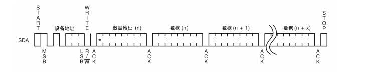
The following figure shows the timing of AT24Cxx byte write mode
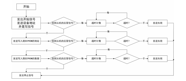
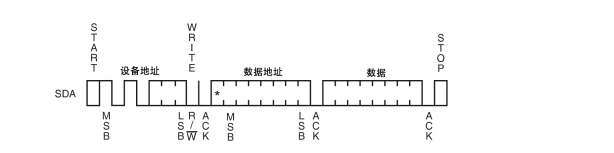 After the MCU sends the Start signal (Start), it sends the 8-bit device address information (the read-write bit in the figure is low level, i.e. write data). After receiving the AT24Cxx response signal, it sends the data address to be written, waits for the AT24Cxx response again, and finally sends the 8-bit data to write data. After the AT24Cxx response, it sends the Stop signal to complete a single word
Section write data.
The capacity of AT24C02 is 2K. Therefore, the data address range is 0x00~0xFF, i.e. 0 ~ 255. Each data address writes 1Byte every time, i.e. 8bit, which is just 2048bit. For 1K capacity products, the data address range is 0x00 ~ 0x7F, and the highest bit will not be used. Therefore, the highest bit of the data address in the figure below is represented by "*", which means that you don't care and won't use it
The timing of AT24Cxx's page write mode is shown in the following figure. The difference between AT24Cxx and Byte write mode is that it does not only send Byte data, but any number of data. It should be noted that this mode cannot write across pages. When across pages are encountered, it is necessary to resend the complete timing.
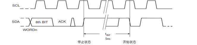
 It is worth mentioning that "AT24Cxx.pdf" mentioned that after each write, and then before the next write, it needs an interval of 5ms to ensure that the last write operation is completed inside the chip
Read AT24Cxx
AT24Cxx supports current address reading mode, random address reading mode and sequential address reading mode.
Current address read mode: continue to read data at the last position after the last read / write operation. For example, the last read / write is at address n, and then the data can be directly divided from n+1;
Random address reading mode: specify the data address and then read the data;
Sequential reading mode: multiple data are read out continuously.
In the current address read mode, there is no need to send the data address. The data address is the position after the last read / write operation, as shown below
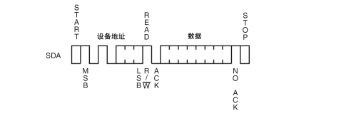 Note: after the host receives the data, there is no need to generate a response signal.
In the random address reading mode, you need to send the device address and the data address to be read first, and then send the signal again to the device address and read the data
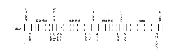
In the sequential read mode, you need to start from the current address read mode or random address read mode, and then you can read multiple data continuously. The sequence is as follows
IIC analog hardware design
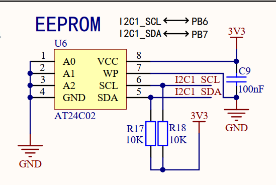 U6 is an AT24C02 chip, and its A0, A1 and A2 are grounded. Therefore, the address of the device is "1010 000X". When reading the device, X is 1, and when writing the device, X is 0.
Pin 7 of U4 is a Write Protect pin (WP). When this pin is high, it is forbidden to write AT24C02. Here, pull down WP directly and write AT24C02 directly at any time.
In addition, both SCL and SDA pins of I2C are pulled up, so as to ensure that both wires must be at high level when I2C bus is idle.
If there is no pull-up, release the SDA after the host sends the data. At this time, the level state of SDA is uncertain, which may be high or low. It is impossible to determine whether the slave pulls down and gives the response signal.
IIC simulation software design
Simulate I2C bus timing through GPIO to read and write EEPROM device AT24C02.
- Pin initialization: GPIO port clock enable, GPIO pin set to input / output mode (PB6, PB7);
- Encapsulate the timing function of each link of I2C: start signal, response signal, read-write data and stop signal;
- Use I2C protocol function to read and write AT24C02;
- The main function writes AT24C02 once every time you press the key, and then reads it to verify whether it is consistent with the written data;
Source code analysis
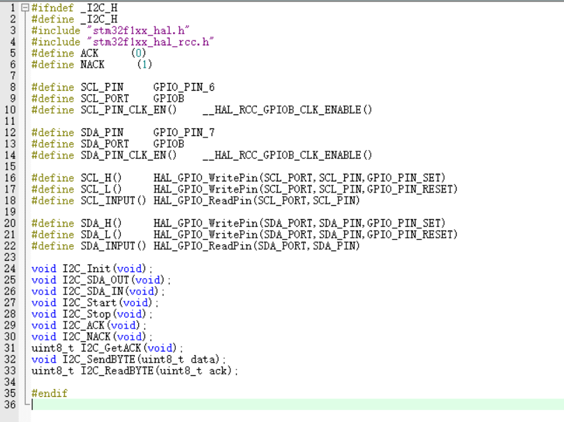
i2c.h
i2c.c
#include <stdio.h>
#include "i2c.h"
#include "main.h"
#include "timer.h"
#include "usart.h"

#define I2C_Delay()     us_timer_delay(5)

//The pin of the initialization analog I2C is in the output state, and both SCL/SDA are initially at the high level
void I2C_Init(void){
    GPIO_InitTypeDef GPIO_InitStruct={0};
    SCL_PIN_CLK_EN();
    SDA_PIN_CLK_EN();

    GPIO_InitStruct.Mode=GPIO_MODE_OUTPUT_PP;
    GPIO_InitStruct.Pull=GPIO_NOPULL;
    GPIO_InitStruct.Pin=SCL_PIN;
    GPIO_InitStruct.Speed=GPIO_SPEED_FREQ_HIGH;

    HAL_GPIO_Init(SCL_PORT,&GPIO_InitStruct);

    GPIO_InitStruct.Pin=SDA_PIN;
    HAL_GPIO_Init(SDA_PORT,&GPIO_InitStruct);

    SCL_H();
    SDA_H();
}

//Configure SDA pin as output.

static void I2C_SDA_OUT(void){
    GPIO_InitTypeDef GPIO_InitStruct={0};

    GPIO_InitStruct.Mode=GPIO_MODE_OUTPUT_PP;
    GPIO_InitStruct.Pull=GPIO_PULLUP;
    GPIO_InitStruct.Speed=GPIO_SPEED_FREQ_HIGH;
    GPIO_InitStruct.Pin=SDA_PIN;

    HAL_GPIO_Init(SDA_PORT,&GPIO_InitStruct);
}
//Configure SDA pin as input mode
static void I2C_SDA_IN(void){
    GPIO_InitTypeDef GPIO_InitStruct={0};
    GPIO_InitStruct.Mode=GPIO_MODE_INPUT;
    GPIO_InitStruct.Speed=GPIO_SPEED_FREQ_HIGH;
    GPIO_InitStruct.Pin=SDA_PIN;

    HAL_GPIO_Init(SDA_PORT,&GPIO_InitStruct);
}
//Start signal
void I2C_Start(void){
    I2C_SDA_OUT();//Set to output mode

    SCL_H();//Clock line output is high
    I2C_Delay();//Delay 5ms

    SDA_H();//Data line output is high
    I2C_Delay();

    SDA_L();//The data line output is low, from high to bottom, indicating the start signal
    I2C_Delay();
}
//End signal
void I2C_Stop(void){
    I2C_SDA_OUT();//Output mode

    SDA_L();
    I2C_Delay();

    SCL_H();
    I2C_Delay();

    SDA_H();
    I2C_Delay();
}
//Send response signal function
void I2C_ACK(void){
    I2C_SDA_OUT();//Set to receive mode

    SCL_L();//Clock line output is low
    I2C_Delay();

    SDA_L();
    I2C_Delay();

    SCL_H();
    I2C_Delay();

    SCL_L();
    I2C_Delay();

}
//Send non response signal
void I2C_NACK(void){
    I2C_SDA_OUT();

    SCL_L();
    I2C_Delay();

    SDA_H();
    I2C_Delay();

    SCL_H();
    I2C_Delay();

    SCL_L();
    I2C_Delay();
}

//Wait for the response signal from the slave
uint8_t I2C_GetACK(void){
    uint8_t time=0;

    I2C_SDA_IN();//Set to input mode

    SCL_L();
    I2C_Delay();

    SDA_H();
    I2C_Delay();

    SCL_H();
    I2C_Delay();

    while(SDA_INPUT()){
        time++;
        if(time>250){
            SCL_L();
            return 1;
        }
    }
    SCL_L();
    return 0;
}

//Send one byte of data
void I2C_SendBYTE(uint8_t data){
    uint8_t cnt=0;

    I2C_SDA_OUT();

    for(cnt=0;cnt<8;cnt++){
        SCL_L();
        I2C_Delay();

        if(data & 0x80){
            SDA_H();
        }else{
            SDA_L();
        }
        data<<=1;

        SCL_H();
        I2C_Delay();
    }
    SCL_L();//Send data
    I2C_Delay();
    I2C_GetACK();
}

//Read one byte of data

uint8_t I2C_ReadBYTE(uint8_t ack){
    uint8_t cnt=0;
    uint8_t data=0xFF;//Determine the value of data

    SCL_L();
    I2C_Delay();

    for(cnt=0;cnt<8;cnt++){
        SCL_H();  //SCL high, read data
        I2C_Delay();

        data<<=1;

        if(SDA_INPUT()){
            data |=0x01;
        }
        SCL_L();
        I2C_Delay();
    }
    //Send response signal, low is response, high is non response
    if(ack==0){
        I2C_ACK();
    }
    else{
        I2C_NACK();
    }
    return data;
}
eeprom.h
#ifndef _EEPROM_H
#define _EEPROM_H
#include "stm32f1xx_hal.h"

#define EEPROM_DEV_ADDR     (0xA0)
#define EEPROM_WR           (0x00)
#define EEPROM_RD           (0x01)

#define EEPROM_WORD_ADDR_SIZE   (0x08)


void EEPROM_WriteByte(uint16_t addr,uint8_t data);
void EEPROM_ReadByte(uint16_t addr,uint8_t *pdata);
void EEPROM_Write_NByte(uint16_t addr , uint8_t *pdata,uint16_t size);
void EEPROM_Read_NByte(uint16_t addr,uint8_t *pdata,uint16_t size);
#endif
eerom.c
#include "eeprom.h"
#include <stdio.h>
#include"gpio.h"
#include "usart.h"
#include "i2c.h"
#include "timer.h"

//EEPROM writes a byte
void EEPROM_WriteByte(uint16_t addr,uint8_t data){
    //Start signal
    I2C_Start();

    //Send device address to write
    I2C_SendBYTE(EEPROM_DEV_ADDR | EEPROM_WR);

    //Data address to write
    if(EEPROM_WORD_ADDR_SIZE==0x08){
        I2C_SendBYTE((uint8_t)(addr & 0x00FF));
    }
    else{
        I2C_SendBYTE((uint8_t)(addr>>8));
        I2C_SendBYTE((uint8_t)(addr & 0x00FF));
    }

    //Write data
    I2C_SendBYTE(data);

    //Stop signal
    I2C_Stop();
}

//Read a byte of EEPROM
void EEPROM_ReadByte(uint16_t addr,uint8_t *pdata){
    //Start signal
    I2C_Start();

    //Device address
    I2C_SendBYTE(EEPROM_DEV_ADDR | EEPROM_WR);

    //Address of data read
    if(EEPROM_WORD_ADDR_SIZE==0x08){
        I2C_SendBYTE((uint8_t)(addr & 0x00FF));
    }else{
        I2C_SendBYTE((uint8_t)(addr>>8));
        I2C_SendBYTE((uint8_t)(addr & 0x00ff));
    }

    //Start transmission
    I2C_Start();

    //Address of the device and set to read mode
    I2C_SendBYTE(EEPROM_DEV_ADDR | EEPROM_RD);

    //Read data because reading data does not require a response signal
    *pdata=I2C_ReadBYTE(NACK);

    //end
    I2C_Stop();
}

//Write N bytes
void EEPROM_Write_NByte(uint16_t addr , uint8_t *pdata,uint16_t size){
    uint16_t i=0;

    for(i=0;i<size;i++){
        EEPROM_WriteByte(addr,pdata[i]);
        addr++;
        HAL_Delay(10);//Each time, it needs to be delayed for 5ms. Here, it needs to be delayed for 10ms to prevent errors
    }
}
//Continuous data reading
void EEPROM_Read_NByte(uint16_t addr,uint8_t *pdata,uint16_t size){

    uint16_t i=0;
    for(i=0;i<size;i++){
        EEPROM_ReadByte(addr,&pdata[i]);
        addr++;
    }
}
timer.h
#ifndef _TIMER_H
#define _TIMER_H

#include "stm32f1xx_hal.h"

void us_timer_delay(uint16_t t);

#endif
timer.c
#include "timer.h"

void us_timer_delay(uint16_t t){
    uint16_t counter=0;
    while(t--){
     counter=10;
     while(counter--){
     }
    }
}
main.c
/* USER CODE BEGIN Header */
/**
  ******************************************************************************
  * @file           : main.c
  * @brief          : Main program body
  ******************************************************************************
  * @attention
  *
  * Copyright (c) 2022 STMicroelectronics.
  * All rights reserved.
  *
  * This software is licensed under terms that can be found in the LICENSE file
  * in the root directory of this software component.
  * If no LICENSE file comes with this software, it is provided AS-IS.
  *
  ******************************************************************************
  */
/* USER CODE END Header */
/* Includes ------------------------------------------------------------------*/
#include "main.h"
#include "usart.h"
#include "gpio.h"

/* Private includes ----------------------------------------------------------*/
/* USER CODE BEGIN Includes */
#include "eeprom.h"
#include<stdio.h>
#include "i2c.h"
#include "timer.h"
#include "string.h"
/* USER CODE END Includes */

/* Private typedef -----------------------------------------------------------*/
/* USER CODE BEGIN PTD */

/* USER CODE END PTD */

/* Private define ------------------------------------------------------------*/
/* USER CODE BEGIN PD */
/* USER CODE END PD */

/* Private macro -------------------------------------------------------------*/
/* USER CODE BEGIN PM */

/* USER CODE END PM */

/* Private variables ---------------------------------------------------------*/

/* USER CODE BEGIN PV */

/* USER CODE END PV */

/* Private function prototypes -----------------------------------------------*/
void SystemClock_Config(void);
static void MX_NVIC_Init(void);
/* USER CODE BEGIN PFP */

/* USER CODE END PFP */

/* Private user code ---------------------------------------------------------*/
/* USER CODE BEGIN 0 */

/* USER CODE END 0 */

/**
  * @brief  The application entry point.
  * @retval int
  */
int main(void)
{
  /* USER CODE BEGIN 1 */
char tx_buffer[20]={"Hello IIC"};
char rx_buffer[20]={0};
  /* USER CODE END 1 */

  /* MCU Configuration--------------------------------------------------------*/

  /* Reset of all peripherals, Initializes the Flash interface and the Systick. */
  HAL_Init();

  /* USER CODE BEGIN Init */

  /* USER CODE END Init */

  /* Configure the system clock */
  SystemClock_Config();

  /* USER CODE BEGIN SysInit */

  /* USER CODE END SysInit */

  /* Initialize all configured peripherals */
  MX_GPIO_Init();
  MX_USART1_UART_Init();

  /* Initialize interrupts */
  MX_NVIC_Init();
  /* USER CODE BEGIN 2 */
printf("*****************\r\n");
printf("i2c test\r\n");
printf("*****************\r\n");
  /* USER CODE END 2 */

  /* Infinite loop */
  /* USER CODE BEGIN WHILE */
  while (1)
  {
    /* USER CODE END WHILE */

    /* USER CODE BEGIN 3 */
      if(get_KeyValue()){
      //Read / write string and print
            EEPROM_Write_NByte(0,(uint8_t *)tx_buffer,sizeof(tx_buffer));
            HAL_Delay(1);

            EEPROM_Read_NByte(0,(uint8_t *)rx_buffer,sizeof(rx_buffer));
            HAL_Delay(1);

          printf("EEPROM Write :%s\r\n",rx_buffer);
          printf("EEPROM Read :%s\r\n",rx_buffer);

          //Clear the receive buffer
          memset(rx_buffer,0,sizeof(rx_buffer));
      }
  }
  /* USER CODE END 3 */
}

/**
  * @brief System Clock Configuration
  * @retval None
  */
void SystemClock_Config(void)
{
  RCC_OscInitTypeDef RCC_OscInitStruct = {0};
  RCC_ClkInitTypeDef RCC_ClkInitStruct = {0};

  /** Initializes the RCC Oscillators according to the specified parameters
  * in the RCC_OscInitTypeDef structure.
  */
  RCC_OscInitStruct.OscillatorType = RCC_OSCILLATORTYPE_HSE;
  RCC_OscInitStruct.HSEState = RCC_HSE_ON;
  RCC_OscInitStruct.HSEPredivValue = RCC_HSE_PREDIV_DIV1;
  RCC_OscInitStruct.HSIState = RCC_HSI_ON;
  RCC_OscInitStruct.PLL.PLLState = RCC_PLL_ON;
  RCC_OscInitStruct.PLL.PLLSource = RCC_PLLSOURCE_HSE;
  RCC_OscInitStruct.PLL.PLLMUL = RCC_PLL_MUL9;
  if (HAL_RCC_OscConfig(&RCC_OscInitStruct) != HAL_OK)
  {
    Error_Handler();
  }
  /** Initializes the CPU, AHB and APB buses clocks
  */
  RCC_ClkInitStruct.ClockType = RCC_CLOCKTYPE_HCLK|RCC_CLOCKTYPE_SYSCLK
                              |RCC_CLOCKTYPE_PCLK1|RCC_CLOCKTYPE_PCLK2;
  RCC_ClkInitStruct.SYSCLKSource = RCC_SYSCLKSOURCE_PLLCLK;
  RCC_ClkInitStruct.AHBCLKDivider = RCC_SYSCLK_DIV1;
  RCC_ClkInitStruct.APB1CLKDivider = RCC_HCLK_DIV2;
  RCC_ClkInitStruct.APB2CLKDivider = RCC_HCLK_DIV1;

  if (HAL_RCC_ClockConfig(&RCC_ClkInitStruct, FLASH_LATENCY_2) != HAL_OK)
  {
    Error_Handler();
  }
}

/**
  * @brief NVIC Configuration.
  * @retval None
  */
static void MX_NVIC_Init(void)
{
  /* EXTI0_IRQn interrupt configuration */
  HAL_NVIC_SetPriority(EXTI0_IRQn, 1, 0);
  HAL_NVIC_EnableIRQ(EXTI0_IRQn);
  /* USART1_IRQn interrupt configuration */
  HAL_NVIC_SetPriority(USART1_IRQn, 0, 0);
  HAL_NVIC_EnableIRQ(USART1_IRQn);
}

/* USER CODE BEGIN 4 */

/* USER CODE END 4 */

/**
  * @brief  This function is executed in case of error occurrence.
  * @retval None
  */
void Error_Handler(void)
{
  /* USER CODE BEGIN Error_Handler_Debug */
  /* User can add his own implementation to report the HAL error return state */
  __disable_irq();
  while (1)
  {
  }
  /* USER CODE END Error_Handler_Debug */
}

#ifdef  USE_FULL_ASSERT
/**
  * @brief  Reports the name of the source file and the source line number
  *         where the assert_param error has occurred.
  * @param  file: pointer to the source file name
  * @param  line: assert_param error line source number
  * @retval None
  */
void assert_failed(uint8_t *file, uint32_t line)
{
  /* USER CODE BEGIN 6 */
  /* User can add his own implementation to report the file name and line number,
     ex: printf("Wrong parameters value: file %s on line %d\r\n", file, line) */
  /* USER CODE END 6 */
}
#endif /* USE_FULL_ASSERT */
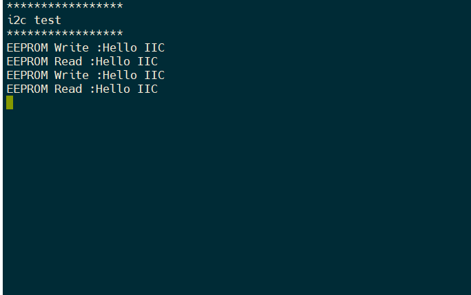
Operation results