The following content is based on stm32f103c8t6 blue hill board + OV7670 camera (with AL422B FIFO module).
At present, I use STM32 IO port resources as follows:
PA9, PA10 for USART1;
PB10, PB11 for SCCB (I2C)
PA0~PA7 are used for D0-D7 data transmission;
PB0 is used for PWDN pin configuration (set Normal or Power Down Mode);
PB1 is used for RESET pin configuration;
PB6 is used for VSYNC pin acquisition (i.e. frame synchronization signal acquisition);
PB7 is used to capture the line synchronization signal;
PB8 is used for FIFO WR pin configuration (i.e. control write enable to FIFO);
PB9 is used for FIFO WRST pin configuration (i.e. write reset of control to FIFO);
PC13 is used for FIFO RCK pin configuration (i.e. providing read clock from FIFO);
PC14 is used for FIFO OE pin configuration (i.e. control read enable from FIFO);
PC15 is used for FIFO RRST pin configuration (i.e. control read reset from FIFO);
Note that in the IO port of STM32F103C8T6 series, PB3/PB4/PA13/PA14/PA15 are all JTAG functions by default. It is recommended that they should not be used. If they need to be used, they can be pulled down / up normally after remapping. You can refer to the introduction of the following blog: On the problem that the pin of PB3/PB4/PA13/PA14/PA15 of STM32 can not control the output
The process of my driver development is as follows: first, verify whether the SCCB communication with the camera is normal - > verify whether the write / read operation from FIFO is correct through the output of 8-color bar - > verify the camera image transmission function. The following code will be interpreted in this order.
First of all, the code is the RCC configuration of various peripherals. There should not be too much to explain. As long as the peripherals need to be used, they need to turn on the corresponding RCC clock. It should be noted that do not forget to initialize the RCC clock of AFIO. This is needed when the IO port needs to be used as a specific pin of some peripherals.
void RCC_Config(void){
	RCC_APB1PeriphClockCmd(RCC_APB1Periph_I2C2,ENABLE);
	RCC_APB2PeriphClockCmd(RCC_APB2Periph_GPIOA,ENABLE);
	RCC_APB2PeriphClockCmd(RCC_APB2Periph_GPIOB,ENABLE);
	RCC_APB2PeriphClockCmd(RCC_APB2Periph_GPIOC,ENABLE);
	RCC_APB2PeriphClockCmd(RCC_APB2Periph_AFIO,ENABLE);
	RCC_APB2PeriphClockCmd(RCC_APB2Periph_USART1,ENABLE);
}
Next is the configuration of GPIO. Different interfaces of each peripheral require different input / output configurations for GPIO. For details, please refer to section 9.1.11 of STM32 reference manual for detailed configuration instructions. Later, when we talk about each module, we will make further instructions on the GPIO port configuration.
void GPIO_Config(void){
	// for USART1; PA9-TX, PA10-RX
	GPIO_InitStructure.GPIO_Mode = GPIO_Mode_AF_PP;
	GPIO_InitStructure.GPIO_Pin = GPIO_Pin_9;
	GPIO_InitStructure.GPIO_Speed = GPIO_Speed_50MHz;
	GPIO_Init(GPIOA, &GPIO_InitStructure);

	GPIO_InitStructure.GPIO_Mode = GPIO_Mode_IN_FLOATING;
	GPIO_InitStructure.GPIO_Pin = GPIO_Pin_10;
	GPIO_Init(GPIOA, &GPIO_InitStructure);

	// for I2C2; PB10-I2C_SCL, PB11-I2C_SDA
	GPIO_InitStructure.GPIO_Mode = GPIO_Mode_AF_OD;
	GPIO_InitStructure.GPIO_Pin = GPIO_Pin_10;
	GPIO_InitStructure.GPIO_Speed = GPIO_Speed_50MHz;
	GPIO_Init(GPIOB, &GPIO_InitStructure);

	GPIO_InitStructure.GPIO_Mode = GPIO_Mode_AF_OD;
	GPIO_InitStructure.GPIO_Pin = GPIO_Pin_11;
	GPIO_InitStructure.GPIO_Speed = GPIO_Speed_50MHz;
	GPIO_Init(GPIOB, &GPIO_InitStructure);

	// for PWDN, RESET; PB0 - PWDN, PB5 - RESET
	GPIO_InitStructure.GPIO_Mode = GPIO_Mode_Out_PP;
	GPIO_InitStructure.GPIO_Pin = OV_PWDN;
	GPIO_InitStructure.GPIO_Speed = GPIO_Speed_50MHz;
	GPIO_Init(GPIOB, &GPIO_InitStructure);

	GPIO_InitStructure.GPIO_Mode = GPIO_Mode_Out_PP;
	GPIO_InitStructure.GPIO_Pin = OV_RESET;
	GPIO_InitStructure.GPIO_Speed = GPIO_Speed_50MHz;
	GPIO_Init(GPIOB, &GPIO_InitStructure);

	// for HREF, VSYNC; PB6 - VSYNC, PB7 - HREF
	GPIO_InitStructure.GPIO_Mode = GPIO_Mode_IN_FLOATING;
	GPIO_InitStructure.GPIO_Pin = OV_VSYNC;
	GPIO_Init(GPIOB, &GPIO_InitStructure);
	GPIO_EXTILineConfig(GPIO_PortSourceGPIOB, GPIO_PinSource6);

	GPIO_InitStructure.GPIO_Mode = GPIO_Mode_IN_FLOATING;
	GPIO_InitStructure.GPIO_Pin = OV_HREF;
	GPIO_Init(GPIOB, &GPIO_InitStructure);

	// for WR, WRRST; PB8 - WR ENABLE, PB9 - WR RST
	GPIO_InitStructure.GPIO_Mode = GPIO_Mode_Out_PP;
	GPIO_InitStructure.GPIO_Pin = FIFO_WR;
	GPIO_InitStructure.GPIO_Speed = GPIO_Speed_50MHz;
	GPIO_Init(GPIOB,&GPIO_InitStructure);

	GPIO_InitStructure.GPIO_Mode = GPIO_Mode_Out_PP;
	GPIO_InitStructure.GPIO_Pin = FIFO_WRST;
	GPIO_InitStructure.GPIO_Speed = GPIO_Speed_50MHz;
	GPIO_Init(GPIOB,&GPIO_InitStructure);

	//for RCK, OE and RRST; PC13 - RCK, PC14 - OE, PC15 - RRST
	GPIO_InitStructure.GPIO_Mode = GPIO_Mode_Out_PP;
	GPIO_InitStructure.GPIO_Pin = FIFO_RCK;
	GPIO_InitStructure.GPIO_Speed = GPIO_Speed_50MHz;
	GPIO_Init(GPIOC,&GPIO_InitStructure);

	GPIO_InitStructure.GPIO_Mode = GPIO_Mode_Out_PP;
	GPIO_InitStructure.GPIO_Pin = FIFO_OE;
	GPIO_InitStructure.GPIO_Speed = GPIO_Speed_50MHz;
	GPIO_Init(GPIOC,&GPIO_InitStructure);

	GPIO_InitStructure.GPIO_Mode = GPIO_Mode_Out_PP;
	GPIO_InitStructure.GPIO_Pin = FIFO_RRST;
	GPIO_InitStructure.GPIO_Speed = GPIO_Speed_50MHz;
	GPIO_Init(GPIOC,&GPIO_InitStructure);

	// for Camera Read Port; PA0~7 - D0~D7
	GPIO_InitStructure.GPIO_Mode = GPIO_Mode_IN_FLOATING;
	GPIO_InitStructure.GPIO_Pin = GPIO_Pin_0;
	GPIO_Init(GPIOA,&GPIO_InitStructure);

	GPIO_InitStructure.GPIO_Mode = GPIO_Mode_IN_FLOATING;
	GPIO_InitStructure.GPIO_Pin = GPIO_Pin_1;
	GPIO_Init(GPIOA,&GPIO_InitStructure);

	GPIO_InitStructure.GPIO_Mode = GPIO_Mode_IN_FLOATING;
	GPIO_InitStructure.GPIO_Pin = GPIO_Pin_2;
	GPIO_Init(GPIOA,&GPIO_InitStructure);

	GPIO_InitStructure.GPIO_Mode = GPIO_Mode_IN_FLOATING;
	GPIO_InitStructure.GPIO_Pin = GPIO_Pin_3;
	GPIO_Init(GPIOA,&GPIO_InitStructure);

	GPIO_InitStructure.GPIO_Mode = GPIO_Mode_IN_FLOATING;
	GPIO_InitStructure.GPIO_Pin = GPIO_Pin_4;
	GPIO_Init(GPIOA,&GPIO_InitStructure);

	GPIO_InitStructure.GPIO_Mode = GPIO_Mode_IN_FLOATING;
	GPIO_InitStructure.GPIO_Pin = GPIO_Pin_5;
	GPIO_Init(GPIOA,&GPIO_InitStructure);

	GPIO_InitStructure.GPIO_Mode = GPIO_Mode_IN_FLOATING;
	GPIO_InitStructure.GPIO_Pin = GPIO_Pin_6;
	GPIO_Init(GPIOA,&GPIO_InitStructure);

	GPIO_InitStructure.GPIO_Mode = GPIO_Mode_IN_FLOATING;
	GPIO_InitStructure.GPIO_Pin = GPIO_Pin_7;
	GPIO_Init(GPIOA,&GPIO_InitStructure);
}
After these configurations are completed, we can see how to use SCCB to communicate with camera module: the simplest attempt is to read the ID of the device through SCCB, and then print the returned ID value through serial port to judge whether the reading and writing operation of SCCB communication is correct.
First of all, we need to initialize the USART serial port. The corresponding GPIO configuration is in GPIO_ The config function has been completed. Note that USART TX needs to be configured as Alternate function push-pull instead of push pull output; RX needs to be configured as Input Floating.
The USART serial port is configured as follows, with 115200 baud rate and stop Bits = 1.
void USART1_Config(void){
	USART_InitStructure.USART_BaudRate = 115200;
	USART_InitStructure.USART_HardwareFlowControl = USART_HardwareFlowControl_None;
	USART_InitStructure.USART_Mode = USART_Mode_Tx | USART_Mode_Rx;
	USART_InitStructure.USART_Parity = USART_Parity_No;
	USART_InitStructure.USART_StopBits = USART_StopBits_1;
	USART_InitStructure.USART_WordLength = USART_WordLength_8b;
	USART_Init(USART1,&USART_InitStructure);
	USART_Cmd(USART1,ENABLE);
}
In order to print out the serial port information conveniently, we will rewrite the printf function, so that we can use the printf function directly like C. note that the option "Use Micro LIB" should also be checked in the compile menu Target.
Also note that the USART needs to be checked_ FLAG_ TXE flag bit to ensure USART_SendData is the next byte after sending. Otherwise, the printed information will be incomplete.
int fputc(int ch, FILE *f){
	USART_SendData(USART1,(uint8_t) ch);
	while(USART_GetFlagStatus(USART1,USART_FLAG_TXE) == RESET){};
	return (ch);
}
In this way, the serial port printing is configured and can be verified by any text in printf.
Next is the initialization configuration of SCCB communication. The SCCB communication protocol is basically the same as I2C, so we can use I2C peripheral directly for SCCB communication. The corresponding GPIO is configured in GPIO_ The config function has been completed. Pay attention to GPIO_ In config, the two pins (PB10 and PB11) of I2C need to be configured as alternate function open drain. In this way, we need to increase the pull-up of 3.3V on the pins of PB10 and PB11. Because the open drain mode itself cannot output high level, the pull-up is generally 4.7kohm or 2.2kohm.
The initialization configuration of SCCB (I2C) is as follows: I2C clock rate is configured as 100khz, and there is not much to say about the rest, which are all standard configurations:
void I2C2_Config(void){
	I2C_InitStructure.I2C_Ack = I2C_Ack_Enable;
	I2C_InitStructure.I2C_AcknowledgedAddress = I2C_AcknowledgedAddress_10bit;
	I2C_InitStructure.I2C_ClockSpeed = 100000;
	I2C_InitStructure.I2C_DutyCycle = I2C_DutyCycle_2;
	I2C_InitStructure.I2C_Mode = I2C_Mode_I2C;
	I2C_InitStructure.I2C_OwnAddress1 = 0x01;
	I2C_Init(I2C2,&I2C_InitStructure);
	I2C_Cmd(I2C2, ENABLE);
}
After the configuration of SCCB (I2C) is completed, we will do the read-write function of SCCB. This part is quite important. It is recommended to refer to the OV Serial Camera Control Bus Functional Specification for further understanding.
The first is the write function of SCCB. The actual write operation of SCCB is to refer to the 3-Phase Write Transmission Cycle in the document: write ID address first, then register addresses, and finally write Data. Each phase transmits 1 byte. So SCCB writes functions as follows:
The first step is to check whether SCCB Bus is idle, and check I2C_ FLAG_ The essence of bus implementation is to detect the level on the bus, because the bus level is pulled up to 3.3V in idle time. Step 2: SCCB sends the START flag bit. In fact, it selects Master/Slave mode and checks MASTER_MODE_SELECT event to confirm if timeout (SCCB_TIME_OUT) if the event has not been SET, an error will be returned. The third step is to send ID address. Note that the ID address is different in the read-write state defined by SCCB. Distinguish the read and write operations by the last bit. Check MASTER_TRANSMITTER_MODE_SELECT event to confirm. The fourth step is to send the register address. Note that according to the document description, the sent register address is only valid under the ID address of the write status. Check the MASTER_BYTE_TRANSMITTED event to confirm. The fifth step is to send the data that needs to be written to the register, and also check the MASTER_BYTE_TRANSMITTED event to confirm. The sixth step is to send the STOP flag bit. Note that the SCCB communication protocol only supports writing one byte at a time, so you need to send the STOP bit after writing a byte of data. If you need to write again, you need to repeat the 3-Phase Write Transmission Cycle. This is the whole SCCB write function.
void SCCB_WRITE(uint8_t Reg_Addr, uint8_t Write_Data){

	// Detect the bus is busy or not
	while(I2C_GetFlagStatus(I2C2,I2C_FLAG_BUSY)){};

	// SCCB Generate START
	I2C_GenerateSTART(I2C2,ENABLE);
	SCCB_TIME_OUT = TIME_OUT;
	while(I2C_CheckEvent(I2C2,I2C_EVENT_MASTER_MODE_SELECT) == RESET){
		if((SCCB_TIME_OUT--) == 0){
			printf("\n Start_Event Check Fail");
		}
	}

	// SCCB Send 7-bits Write Address
	I2C_Send7bitAddress(I2C2,SCCB_WRITE_ADDR,I2C_Direction_Transmitter);
	SCCB_TIME_OUT = TIME_OUT;
	while(I2C_CheckEvent(I2C2,I2C_EVENT_MASTER_TRANSMITTER_MODE_SELECTED) == RESET){
		if((SCCB_TIME_OUT--) == 0){
			printf("\n Transmit Address set Fail");
		}
	}

	// SCCB Send Reg Data. Can only be done at WRITE Phase !!!
	I2C_SendData(I2C2,Reg_Addr);
	SCCB_TIME_OUT = TIME_OUT;
	while(I2C_CheckEvent(I2C2,I2C_EVENT_MASTER_BYTE_TRANSMITTED) == RESET){
		if((SCCB_TIME_OUT--) == 0){
			printf("\n Register Address set Fail");
		}
	}

	// SCCB Send Write Data.
	I2C_SendData(I2C2,Write_Data);
	SCCB_TIME_OUT = TIME_OUT;
	while(I2C_CheckEvent(I2C2,I2C_EVENT_MASTER_BYTE_TRANSMITTED) == RESET){
		if((SCCB_TIME_OUT--) == 0){
			printf("\n Write Data Fail");
		}
	}

	// SCCB Generate STOP to end the 3-phase write
	I2C_GenerateSTOP(I2C2,ENABLE);
}
Next is the SCCB read function. According to the description of the reference document, the read operation is 2-phase Write transmission cycle + 2-phase read transmission cycle: first write ID address (write operation), then write the register address to be read, then write ID address (read operation), and finally read the data. Note that the operation to write the register address to be read must follow the ID address of the write operation.
The process from checking whether the bus is busy to sending the STOP flag bit for the first time is the same as the SCCB write function before, so we will not repeat it. After the first STOP flag bit, the first step is to send the START flag bit. Step 2: send the ID address corresponding to the read operation, and check the MASTER_RECEIVER_MODE_SELECTED event to confirm. The third step is that we STOP the Ack and send the STOP flag bit, which is very important!!! Because SCCB only returns one byte for reading, according to STM32 Reference Manual page763, when there is only one byte left to read, Clear ACK, STOP, wait for RXNE flag, and then read. I have measured that if I do not follow this order, SCCB reading will fail. The fourth step is to read the data. When RXNE flag is set up, it can be read. The fifth step is to enable Ack again to prepare for the next reading and writing. This is the reading function of the whole SCCB. The third step is the most important, which must not be ignored.
uint8_t SCCB_READ(uint8_t Reg_Addr){
	uint8_t DATA_REC;

	// Detect the bus is busy or not
	while(I2C_GetFlagStatus(I2C2,I2C_FLAG_BUSY)){};

	// SCCB Generate START
	I2C_GenerateSTART(I2C2,ENABLE);
	SCCB_TIME_OUT = TIME_OUT;
	while(I2C_CheckEvent(I2C2,I2C_EVENT_MASTER_MODE_SELECT) == RESET){
		if((SCCB_TIME_OUT--) == 0){
			printf("\n Start_Event Check Fail");
		}
	}

	// SCCB Send 7-bits Write Address
	I2C_Send7bitAddress(I2C2,SCCB_WRITE_ADDR,I2C_Direction_Transmitter);
	SCCB_TIME_OUT = TIME_OUT;
	while(I2C_CheckEvent(I2C2,I2C_EVENT_MASTER_TRANSMITTER_MODE_SELECTED) == RESET){
		if((SCCB_TIME_OUT--) == 0){
			printf("\n Read T Address set Fail");
		}
	}

	// SCCB Send Reg Data. Can only be done at WRITE Phase !!!
	I2C_SendData(I2C2,Reg_Addr);
	SCCB_TIME_OUT = TIME_OUT;
	while(I2C_CheckEvent(I2C2,I2C_EVENT_MASTER_BYTE_TRANSMITTED) == RESET){
		if((SCCB_TIME_OUT--) == 0){
			printf("\n Register Address set Fail");
		}
	}

	// SCCB Generate STOP to end the 2-phase write
	I2C_GenerateSTOP(I2C2,ENABLE);

	// SCCB Generate START Again
	I2C_GenerateSTART(I2C2,ENABLE);
	SCCB_TIME_OUT = TIME_OUT;
	while(I2C_CheckEvent(I2C2,I2C_EVENT_MASTER_MODE_SELECT) == RESET){
		if((SCCB_TIME_OUT--) == 0){
			printf("\n Start_Event Check Fail");
		}
	}

	// SCCB Send 7-bits Read Address
	I2C_Send7bitAddress(I2C2,SCCB_READ_ADDR,I2C_Direction_Receiver);
	SCCB_TIME_OUT = TIME_OUT;
	while(I2C_CheckEvent(I2C2,I2C_EVENT_MASTER_RECEIVER_MODE_SELECTED) == RESET){
		if((SCCB_TIME_OUT--) == 0){
			printf("\n R Address set Fail");
		}
	}

	// VERY IMPORTANT !!! We need to STOP before the last byte
	I2C_AcknowledgeConfig(I2C2,DISABLE);
	I2C_GenerateSTOP(I2C2,ENABLE);

	// SCCB RECEVIE DATA
	SCCB_TIME_OUT = TIME_OUT;
	while(I2C_GetFlagStatus(I2C2,I2C_FLAG_RXNE) == RESET){
		if((SCCB_TIME_OUT--)==0){
			printf("\n Receive Fail");
		}
	}
	DATA_REC = I2C_ReceiveData(I2C2);

	// SCCB enable ACK for next transmission
	I2C_AcknowledgeConfig(I2C2,ENABLE);

	return DATA_REC;
}
Now that we have finished the read-write function of SCCB, we can verify whether SCCB communication is normal by reading the ID of camera. Before that, we need to pay attention to a pit, that is, after we power on STM32 and the camera, because we have no control over the power on sequence, we must first reset the camera after STM32 runs, and wait for at least 1s for SCCB read-write operation after reset, so as to ensure the normal communication of SCCB; if not reset, it is likely that stm32 The camera was not ready when the read-write operation was initiated.
So we reset by pulling the PB1 pin down and then up, and then set the PB0 (PWDN) down to make the camera enter Normal Mode.
    // Reset Camera
	GPIO_ResetBits(GPIOB,OV_RESET);
	Delay_ms(50);
	GPIO_SetBits(GPIOB, OV_RESET);
	Delay_ms(5000);

	// Set Device into Normal Mode
	GPIO_ResetBits(GPIOB,OV_PWDN);
Next, read 0A, 0B, 1C, 1D registers to obtain the Product ID and Manufacturer ID of the camera, and print them out through the Printf function.
	// Read Device ID Information
	Pro_ID_MSB = SCCB_READ(SCCB_READ_PRO_ID_MSB);
	Pro_ID_LSB = SCCB_READ(SCCB_READ_PRO_ID_LSB);
	Manu_ID_MSB = SCCB_READ(SCCB_READ_MANU_ID_MSB);
	Manu_ID_LSB = SCCB_READ(SCCB_READ_MANU_ID_LSB);

	printf("\n The Product ID is: %d %d ", Pro_ID_MSB, Pro_ID_LSB);
	printf("\n The Manufactuer ID is: %d %d ", Manu_ID_MSB, Manu_ID_LSB);
After the above operations, you can see the printed information on the serial port: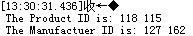
Because the decimal format is printed, the hexadecimal format is as follows:
Product ID: 76 73
Manufactuer ID: 7F A2
As described in OV7670 Datasheet. Prove that SCCB communication between us and the camera is OK.
At this point, we have completed SCCB communication. Next, we can configure the camera through SCCB write function and obtain the data returned by the camera.