catalogue
Liquid crystal control principle
Introduction to ILI9341 LCD controller
Signal line and 8080 timing of LCD
FSMC of STM32 is used to simulate 8080 interface timing
Software design of FSMC control LCD
ILI9341 driver code and ST7789V driver code
Monitor introduction
The display belongs to the I/O device of the computer, that is, the input and output device. It is a display tool that outputs specific electronic information to the screen and then reflects it to the human eye. The common ones are CRT display, LCD display, LED dot matrix display and OLED display.
Liquid crystal display
Compared with the previous generation of CRT display (cathode ray tube display), LCD display has the advantages of low power consumption, small volume, large amount of information and no eye injury. Therefore, it has become the mainstream electronic display equipment.
Basic parameters of display
No matter what kind of display, there are certain parameters to describe their characteristics. The parameters are described as follows:
- Pixel: pixel is the most basic element of the image. The pixel of the display refers to the smallest point of its imaging, that is, a display unit of liquid crystal.
- Resolution: the display of some embedded devices often uses "row pixel value * column pixel value" to indicate the resolution of the screen. For example, the resolution of 800 * 480 indicates that each row of the display has 800 pixels and each column has 400 pixels, which can also be understood as 800 columns and 480 rows
- Color depth: color depth refers to how many colors each pixel of the display can represent, Generally, it is represented by "bit". For example, each pixel of the monochrome screen can represent two states of on or off (that is, it can actually display two colors), and one data bit can represent all States of the pixel, so its color depth is 1bit, and the color depth of other common display screens is 16bit and 24bits
- Display size: the size of the display is generally expressed in inches, such as 5 inches, 21 inches, 24 inches, etc. this length refers to the length of the diagonal of the screen. The actual length and width of the display can be determined through the diagonal length and length width ratio of the display.
- Dot pitch: dot pitch refers to the distance between two adjacent pixels, which will affect the fineness of image quality and viewing distance. For screens of the same size, the higher the resolution, the smaller the dot pitch and the better the image quality. For example, the screen resolution of some mobile phones is larger than that of computer monitors, which is the reason for the small dot pitch of mobile phone screens. The dot pitch of LED dot matrix displays is generally larger, So it is suitable for long-distance viewing.
Liquid crystal control principle
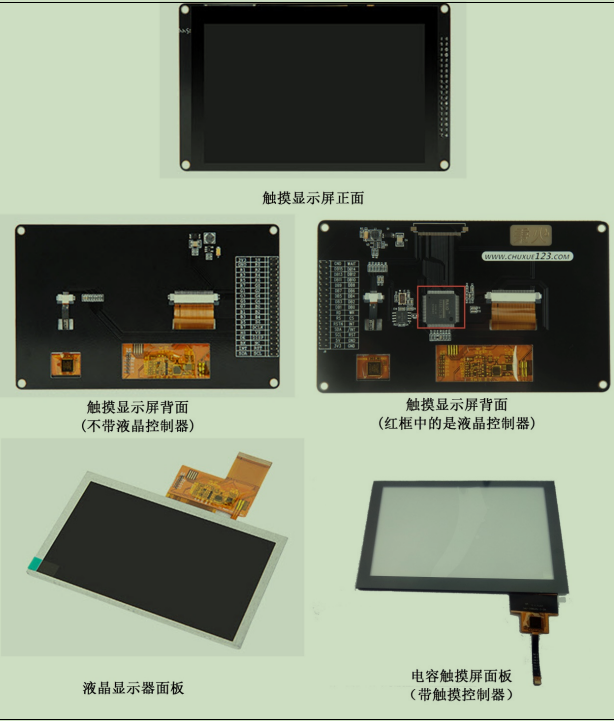
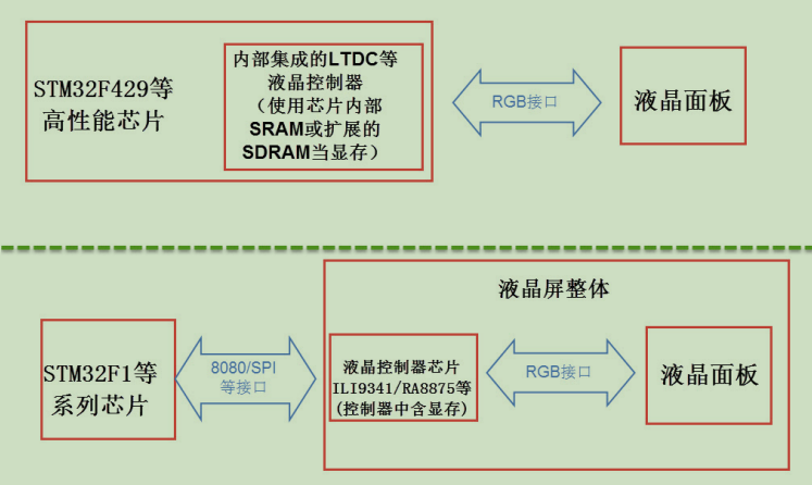
A complete display screen is composed of LCD panel, capacitive touch panel and PCB base plate. The touch panel in the figure is equipped with a touch control chip. The chip processes the touch signal and communicates with external devices through the outgoing signal line. The middle of the touch panel is transparent. It is pasted on the liquid crystal panel to form the main body of the screen together. The flat line led out by the touch panel and the liquid crystal panel is connected to the PCB base plate according to the actual needs, There may be a "LCD" control chip on the PCB base plate ", the LCD panel PCB on the right side of the figure is equipped with a RA8875 LCD controller. Because controlling the LCD panel requires more resources, most low-level microcontrollers cannot directly control the LCD panel, so they need to be equipped with an additional special LCD controller to process the display process. The external microcontroller only needs to directly hand over the data it wants to display to the LCD controller PCB backplane without LCD controller has only a small part of power management circuit. STM32F429 chip does not need additional LCD controller, that is, it integrates the LCD controller into the chip, which can be understood as the CPU integrated graphics card of the computer. STM32F1 series is not integrated, so it needs external connection, which can be understood as the external graphics card of the computer. In general, the control block diagram of these two types of screens is as follows:
Introduction to ILI9341 LCD controller
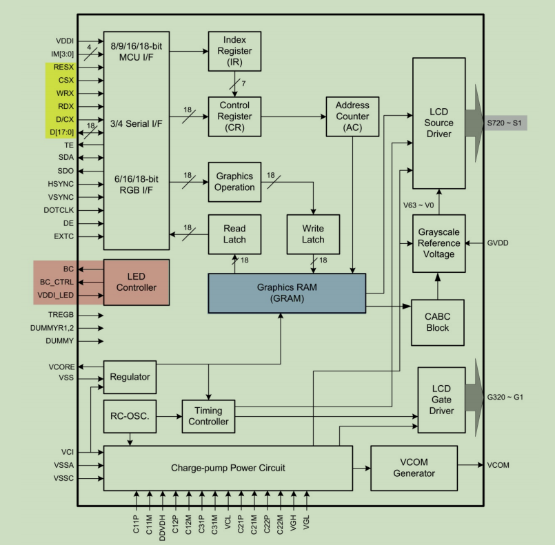
The liquid crystal controller chip used in the experiment is ILI9341. Its internal structure is very complex. See the internal block diagram of ILI9341 controller.
The most important part of the chip is GRAM (Graphics RAM) in the middle, which is video memory. Each storage unit in GRAM corresponds to a pixel on the liquid crystal panel. Various modules on the right side work together to convert the data of GRAM storage unit into the control signal of the liquid crystal panel, so that the pixels present a specific color, and the pixels are combined to form a complete image. The upper left corner of the block diagram is the main control signal line and configuration pin of ILI9341. According to its different state settings, the chip can work in different modes, such as whether the number of bits of each pixel is 6, 16 or 18 bits; It can be configured to use SPI, 8080 interface or RGB interface to communicate with MCU. MCU communicates with ILI9341 through SPI, 8080 interface or RGB interface, so as to access its controller (CR), address counter (AC) and GRAM.
There is also an LED controller on the left side of GRAM. LCD is a non luminous display device, which needs the help of backlight to achieve the display function. LED controller is used to control the LED backlight in LCD screen.
Signal line and 8080 timing of LCD
The ILI9341 controller determines the communication mode between it and MCU according to its IM[3:0] signal line level. It supports SPI and 8080 communication mode. I tested the STM32 board of wildfire. Its ILI9341 controller has been configured as fixed before leaving the factory (internal hardware circuit has been connected). It is configured to communicate through 8080 interface and use the RGB565 format of 16 data lines. After the internal hardware circuit is connected, the remaining signal lines are led out to the FPC flat line. Finally, the flat line is led out from the PCB bottom plate to the flat pin, and then the flat pin is connected with the STM32 chip on the experimental board. The led out flat pin signal line is shown in the signal line led out by the LCD.
| The signal line | Signal line corresponding to ILI9341 | explain |
| LCD_DB[15:0] | D[15:0] | data signal |
| LCD_RD | RDX | Read data signal, active at low level |
| LCD_RS | D/CX | Data / command signal: at high level, D[15:0] represents data (RGB565 pixel data or command data), and at low level, D[15:0] represents control command |
| LCD_RESET | RESX | Reset signal, active at low level |
| LCD_WR | WRX | Write data signal, active at low level |
| LCD_CS | CSX | Chip selection signal, active at low level |
| LCD_BK | - | Backlight signal, low level on |
| GPIO[5:1] | - | Control signal line of touch screen, |
These signal lines are 8080 communication interfaces. The one with X indicates that the low level is effective. STM32 communicates with ILI9341 chip through this interface to realize the control of LCD. The communication content mainly includes commands and display and memory data, which is the data of each pixel; Command refers to the control command of ILI9341. mcu can send command code through 8080 interface to control the working mode of ILI9341, such as reset command, cursor setting command, sleep mode command, etc. for details, please refer to the data manual of ILI9341.
Note: the corresponding control command codes of different LCD control chips here may be different. During my experiment, I thought that the control chip of ILI9341 was on the board, but finally found that the ST7789V control chip was used, so that the color was incorrect and the final configuration was correct.
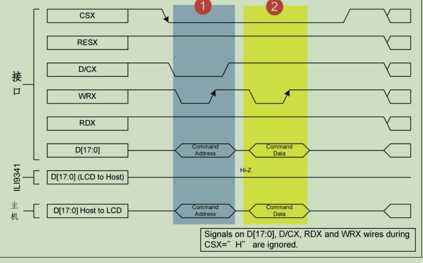
It can be seen from the figure that the write command sequence starts with the chip selection signal CSX pulled low, and the data / command selection signal line D/CX is also set to low level, indicating that the write is the command address (which can be understood as command coding). Taking the write signal WRX as low and the signal RDX as high level indicates that the transmission direction of data is write. At this time, the command address is output on the data line D[15:0], In the second transmission stage, the parameters of the command are transmitted, so D/CX should be set to high level, which means that the written command data refers to the parameters of some instructions. For example, the reset instruction code can be followed by a parameter, which indicates how many seconds to reset.
FSMC of STM32 is used to simulate 8080 interface timing
Introduction to FSMC
FSMC is the peripheral of STM32, which is used to manage the extended memory. FSMC can be used to drive SRAM, NOR FLASH and NAND FLASH memory, but can not drive SDRAM. In STM32F429 series controller, it has FMC peripheral, which can drive SDRAM memory.
Because FSMC peripherals can control the extended external memory, the operation of MCU on LCD screen is actually to write the display data into the display memory, which is very similar to the control memory, and the communication sequence of 8080 interface can be generated by FSMC peripherals.
The structure of FSMC peripherals is shown in the figure
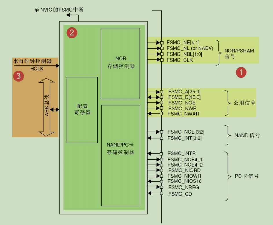
Communication pin
On the right side of the block diagram are the control pins related to FSMC peripherals. Because there are some different pins when controlling different types of memory, it seems that there will be many address lines FSMC_A and data line FSMC_D is shared by all controllers. The specific GPIO ports and pins corresponding to these FSMC pins can be seen in the corresponding manuals.
| FSMC signal name | Signal direction | function |
| CLK | output | Clock (used in synchronous burst mode) |
| A[25:0] | output | Address bus |
| D[15:0] | Input / output | Bidirectional data bus |
| NE[X] | output | Film selection, x=1, 2, 3, 4 |
| NOE | output | Output enable |
| NWE | output | Write enable |
| NWAIT | input | NOR flash requires FSMC to wait for the signal |
| NADV | output | Address, a signal used as a latch when data lines are multiplexed |
When controlling LCD, the NOR FLASH control mode similar to asynchronous and independent of address and data line is used, so in fact, CLK, NWAIT and NADV pins are not used.
Among them, the special FSMC_NE1/2/3/4 pins. Different pins correspond to different control areas in STM32. For example, when STM32 accesses 0x68000000 ~ 0x6bfffffff address space, FSMC_NE3 pin will be automatically set to low level. Since it is generally connected to the chip selection pin of external memory and the low level is effective, chip selection of external memory is enabled. When accessing 0x60000000~0x63FFFFFF address, FSMC_NE1 will output low level. Different fsmcs were used_ When the ne pin is connected to the external memory, the address of STM32 accessing the external memory is different, so as to control multiple external memory chips.
Memory controller
The above different types of pins are connected to the corresponding memory controller inside the FSMC. NOR/PSRAM/SRAM devices use the same controller, NAND/PC card devices use the same controller, and different controllers have special registers to configure their working modes.
FSMC controls NOR FLASH_ Bcr1 / 2 / 3 / 4 control register, FSMC_BTR1/2/3/4 chip selection timing register and FSMC_BWTR1/2/3/4 write timing register. There are 4 registers in each type, which correspond to 4 different storage areas respectively. Various registers are introduced as follows:
- FSMC_BCR control register can configure parameters such as memory type, data line width and signal effective polarity to be controlled
- FSMC_BTR timing register is used to configure various time delays during SRAM access, such as data holding time, address holding time, address establishment time and data establishment time.
- FSMC_BWTR timing register and FSMC_ The parameters controlled by the BTR register are similar. It is specially used to control the allowable time parameters at write time.
Clock control logic
FSMC peripherals are mounted on the AHB bus. The clock signal comes from HCLK, and the default is 72MHZ. The synchronous clock output of the controller is obtained by frequency division. For example, FSMC of nor controller_ The clock output by CLK pin can be used for synchronous communication with NOR FLASH chip of synchronization type, and its clock frequency can be through FSMC_ The CLKDIV bit configuration of BTR register can be configured as 1 / 2 or 1 / 3 of HCLK, that is, if it communicates with NOR FLASH of synchronization type, the maximum frequency of synchronization clock is 36MHZ
FSMC analog 8080 timing
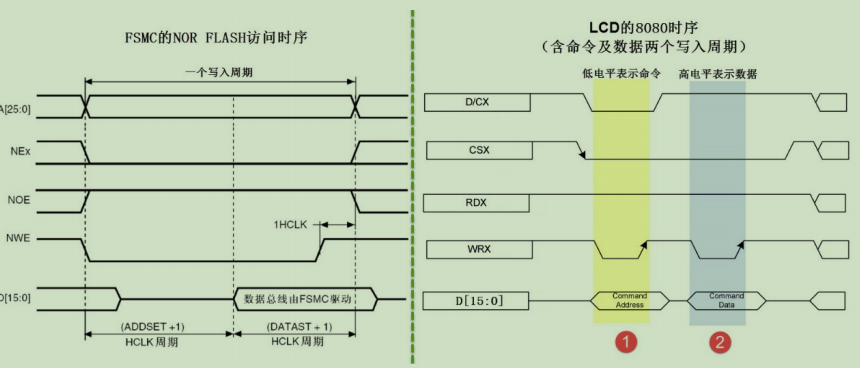
Comparing the mode B timing in FSMC NOR/PSRAM with the 8080 timing of ILI9341 LCD control chip, it can be found that the two timing are very similar, except for the address line A of FSMC and the D/CX line of 8080.
| FSMC_NOR signal line | function | 8080 signal line | function |
| NEx | Chip Select | CSX | Chip Select |
| NWR | Write enable | WRX | Write enable |
| NOE | Read enable | RDX | Read enable |
| D[15:0] | data signal | D[15:0] | data signal |
| A[25:0] | Address signal | A[25:0] | Address signal |
For FSMC and 8080 interfaces, the first four signal lines are exactly the same, except that the address signal line A[25:0] of FSMC is different from the data / command selection line D/CX of 8080. For the D/CX line, when it is high level, it represents the value, and when it is low level, it represents the command. If the A address line of FSMC can be used to generate the corresponding level according to different situations, then FSMC can be used to generate the timing required by 8080 interface.
Software design of FSMC control LCD
Programming points
- Target pin and port clock when initializing communication
- Enable clock of FSMC peripheral
- Configure FSMC as asynchronous NOR FLASH mode to simulate 8080 timing
- Establish a mechanism to send commands and data to the LCD using FSMC
- Send control command to initialize LCD
- Write the drawing pixel function of LCD screen
- Use the point function to make various LCD display applications, such as drawing lines, circles and rectangles
NOR FLASH timing structure
When controlling FSMC to use NOR FLASH memory, it is mainly to configure timing register and control register. It is convenient to write parameters by using the timing structure and initialization structure of ST standard library.
See the code for the members of NOR FLASH timing structure
typedef struct
{
  uint32_t FSMC_AddressSetupTime;    /**Address establishment time 0-0xF HCLK cycles/

  uint32_t FSMC_AddressHoldTime;     /*Address holding time, 0-0xF HCLK cycles*/

  uint32_t FSMC_DataSetupTime;        /*Address establishment time, 0-0xF HCLK cycles*/

  uint32_t FSMC_BusTurnAroundDuration;  /*Bus conversion cycle, 0-0xF HCLK cycles, in NOR FLASH*/

  uint32_t FSMC_CLKDivision;          /*Clock frequency division factor, 1-0xF. If asynchronous memory is controlled, this parameter is invalid*/

  uint32_t FSMC_DataLatency;         /*Data delay time. If asynchronous memory is controlled, this parameter is invalid*/

  uint32_t FSMC_AccessMode;          /*Set access mode*/

}FSMC_NORSRAMTimingInitTypeDef;
This structure is exactly the same as the timing structure in SRAM. The following only lists the description of structure members used in mode B when controlling NOR FLASH:
- FSMC_AddressSetupTime: this member sets the address setup time, that is, FSMC read-write sequence diagram and FSMC write nor_ The ADDSET value in the timing chart of flash can be set to 0-0xF HCLK cycles. According to the default configuration of STM32 standard library, the clock frequency of HCLK is 72MHZ, that is, one HCLK cycle is 1 / 72 microsecond.
- FSMC_DataSetupTime: this member sets the data setup time, that is, the DATAST value in the FSMC read-write timing chart and FSMC write NOR FLASH timing chart. It can be set to 0-0xf HCLK cycles.
- FSMC_BusTurnAroundDuration: this member sets the bus conversion cycle. In NOR FLASH memory, the address line and data line can be time-sharing multiplexed. The bus conversion cycle refers to the delay required for switching between the two states to prevent conflict. This parameter is invalid when controlling other memories. It can be configured as 0.
- FSMC_CLKDivision: this member is used to set the clock frequency division. It takes the HCLK clock as the input and passes through the FSMC_CLKDivision is output to FSMC after frequency division_ CLK pin is used as the synchronous clock for communication. When controlling the memory of other asynchronous communication, this parameter is invalid and can be configured as 0.
- FSMC_DataLatency: this member sets the data retention time, which indicates the number of cycles to wait before reading the first data. This cycle refers to the cycle of the synchronization clock. This parameter is only used to synchronize NOR FLASH memory. When controlling other types of memory, this parameter is invalid. It can be configured as 0.
- FSMC_AccessMode: this member sets the memory access mode. When FSMC accesses the memory address in different modes, the timing of pin output is different. FSMC can be selected_ AccessMode_ A / B / C / D mode, B mode is used when controlling asynchronous NOR FLASH.
This FSMC_NORSRAMTimingInitTypeDef the delay parameter configured in the timing structure will be used as a member of the FSMC NOR FLASH initialization structure.
FSMC structure initialization
typedef struct
{
  uint32_t FSMC_Bank;                /*Set the area to control*/

  uint32_t FSMC_DataAddressMux;     /*Set whether the address bus and data bus are multiplexed*/

  uint32_t FSMC_MemoryType;         /*Set memory type*/

  uint32_t FSMC_MemoryDataWidth;     /*Data width setting of memory*/

  uint32_t FSMC_BurstAccessMode;     /*Set whether burst access mode is supported. Only synchronous memory is supported*/

  uint32_t FSMC_AsynchronousWait;    /*Set whether to enable the waiting signal during synchronous transmission*/

  uint32_t FSMC_WaitSignalPolarity; /*Set the polarity of the waiting signal*/

  uint32_t FSMC_WrapMode;            /*Sets whether aligned burst mode is supported*/

  uint32_t FSMC_WaitSignalActive;    /*Configure whether the waiting signal is valid before waiting or during waiting*/

  uint32_t FSMC_WriteOperation;      /*Set whether to write enable*/

  uint32_t FSMC_WaitSignal;          /*Set whether to wait for status insertion*/

  uint32_t FSMC_ExtendedMode;        /*Set whether it is extensible mode*/

  uint32_t FSMC_WriteBurst;          /*Set whether burst operation can be written*/

  FSMC_NORSRAMTimingInitTypeDef* FSMC_ReadWriteTimingStruct; /*When the extended mode is not used, this parameter is used to configure the read-write timing; otherwise, it is used to configure the read-write timing*/
/*When using extended mode, this parameter is used to configure write timing*/
  FSMC_NORSRAMTimingInitTypeDef* FSMC_WriteTimingStruct;
}FSMC_NORSRAMInitTypeDef;
For this structure, except that the last two members are the timing configuration explained above, the configuration of other structure members corresponds to FSMC_ The register bits in BCR and the meanings of each member are introduced as follows:
(1)FSMC_Bank
This member is used to select the storage area mapped by FSMC, its optional parameters and the address range corresponding to the storage area and area that can be selected in the corresponding kernel address mapping range table.
| Macros that can be imported | Corresponding address area |
| FSMC_Bank1_NORSRAM1 | 0x60000000-0x63FFFFFF |
| FSMC_Bank1_NORSRAM2 | 0x64000000-0x67FFFFFF |
| FSMC_Bank1_NORSRAM3 | 0x68000000-0x6BFFFFFF |
| FSMC_Bank1_NORSRAM4 | 0x6C000000-0x6FFFFFFF |
(2)FSMC_DataAddressMux
This member is used to set whether the address bus and data bus are multiplexed. When controlling NOR FLASH, the address bus and data bus can be multiplexed in time-sharing, which can reduce the number of STM32 signal lines.
(3)FSMC_MemoryType
This member is used to set the memory type to be controlled. The supported memory types are SRAM,PSRAM and NOR FLASH
(4)FSMC_MemoryDataWidth
This member is used to set the data width of the memory to be controlled, which can be optionally set to 8 / 16 bits
(5)FSMC_BurstAccessMode
This member is used to set whether to use the burst access mode. The burst access mode refers to the continuous access to multiple data after sending an address. In the non burst mode, an address needs to be entered for each data access. The burst mode can be used only when controlling the memory of synchronization type.
ILI9341 driver code and ST7789V driver code
ILI9341 Driver code: This is the official driver code given by the official
 /*  Power control B (CFh)  */
    DEBUG_DELAY  ();
    ILI9341_Write_Cmd ( 0xCF  );
    ILI9341_Write_Data ( 0x00  );
    ILI9341_Write_Data ( 0x81  );
    ILI9341_Write_Data ( 0x30  );

    /*  Power on sequence control (EDh) */
    DEBUG_DELAY ();
    ILI9341_Write_Cmd ( 0xED );
    ILI9341_Write_Data ( 0x64 );
    ILI9341_Write_Data ( 0x03 );
    ILI9341_Write_Data ( 0x12 );
    ILI9341_Write_Data ( 0x81 );

    /*  Driver timing control A (E8h) */
    DEBUG_DELAY ();
    ILI9341_Write_Cmd ( 0xE8 );
    ILI9341_Write_Data ( 0x85 );
    ILI9341_Write_Data ( 0x10 );
    ILI9341_Write_Data ( 0x78 );

    /*  Power control A (CBh) */
    DEBUG_DELAY ();
    ILI9341_Write_Cmd ( 0xCB );
    ILI9341_Write_Data ( 0x39 );
    ILI9341_Write_Data ( 0x2C );
    ILI9341_Write_Data ( 0x00 );
    ILI9341_Write_Data ( 0x34 );
    ILI9341_Write_Data ( 0x03 );

    /* Pump ratio control (F7h) */
    DEBUG_DELAY ();
    ILI9341_Write_Cmd ( 0xF7 );
    ILI9341_Write_Data ( 0x20 );

    /* Driver timing control B */
    DEBUG_DELAY ();
    ILI9341_Write_Cmd ( 0xEA );
    ILI9341_Write_Data ( 0x00 );
    ILI9341_Write_Data ( 0x00 );

    /* Frame Rate Control (In Normal Mode/Full Colors) (B1h) */
    DEBUG_DELAY ();
    ILI9341_Write_Cmd ( 0xB1 );
    ILI9341_Write_Data ( 0x00 );
    ILI9341_Write_Data ( 0x1B );

    /*  Display Function Control (B6h) */
    DEBUG_DELAY ();
    ILI9341_Write_Cmd ( 0xB6 );
    ILI9341_Write_Data ( 0x0A );
    ILI9341_Write_Data ( 0xA2 );

    /* Power Control 1 (C0h) */
    DEBUG_DELAY ();
    ILI9341_Write_Cmd ( 0xC0 );
    ILI9341_Write_Data ( 0x35 );

    /* Power Control 2 (C1h) */
    DEBUG_DELAY ();
    ILI9341_Write_Cmd ( 0xC1 );
    ILI9341_Write_Data ( 0x11 );

    /* VCOM Control 1 (C5h) */
    ILI9341_Write_Cmd ( 0xC5 );
    ILI9341_Write_Data ( 0x45 );
    ILI9341_Write_Data ( 0x45 );

    /*  VCOM Control 2 (C7h)  */
    ILI9341_Write_Cmd ( 0xC7 );
    ILI9341_Write_Data ( 0xA2 );

    /* Enable 3G (F2h) */
    ILI9341_Write_Cmd ( 0xF2 );
    ILI9341_Write_Data ( 0x00 );

    /* Gamma Set (26h) */
    ILI9341_Write_Cmd ( 0x26 );
    ILI9341_Write_Data ( 0x01 );
    DEBUG_DELAY ();

    /* Positive Gamma Correction */
    ILI9341_Write_Cmd ( 0xE0 ); //Set Gamma
    ILI9341_Write_Data ( 0x0F );
    ILI9341_Write_Data ( 0x26 );
    ILI9341_Write_Data ( 0x24 );
    ILI9341_Write_Data ( 0x0B );
    ILI9341_Write_Data ( 0x0E );
    ILI9341_Write_Data ( 0x09 );
    ILI9341_Write_Data ( 0x54 );
    ILI9341_Write_Data ( 0xA8 );
    ILI9341_Write_Data ( 0x46 );
    ILI9341_Write_Data ( 0x0C );
    ILI9341_Write_Data ( 0x17 );
    ILI9341_Write_Data ( 0x09 );
    ILI9341_Write_Data ( 0x0F );
    ILI9341_Write_Data ( 0x07 );
    ILI9341_Write_Data ( 0x00 );

    /* Negative Gamma Correction (E1h) */
    ILI9341_Write_Cmd ( 0XE1 ); //Set Gamma
    ILI9341_Write_Data ( 0x00 );
    ILI9341_Write_Data ( 0x19 );
    ILI9341_Write_Data ( 0x1B );
    ILI9341_Write_Data ( 0x04 );
    ILI9341_Write_Data ( 0x10 );
    ILI9341_Write_Data ( 0x07 );
    ILI9341_Write_Data ( 0x2A );
    ILI9341_Write_Data ( 0x47 );
    ILI9341_Write_Data ( 0x39 );
    ILI9341_Write_Data ( 0x03 );
    ILI9341_Write_Data ( 0x06 );
    ILI9341_Write_Data ( 0x06 );
    ILI9341_Write_Data ( 0x30 );
    ILI9341_Write_Data ( 0x38 );
    ILI9341_Write_Data ( 0x0F );

    /* memory access control set */
    DEBUG_DELAY ();
    ILI9341_Write_Cmd ( 0x36 );
    ILI9341_Write_Data ( 0xC8 );    /*Scanning mode from the upper left corner (starting point) to the lower right corner (end point) of the vertical screen*/
    DEBUG_DELAY ();

    /* column address control set */
    ILI9341_Write_Cmd ( CMD_SetCoordinateX );
    ILI9341_Write_Data ( 0x00 );
    ILI9341_Write_Data ( 0x00 );
    ILI9341_Write_Data ( 0x00 );
    ILI9341_Write_Data ( 0xEF );

    /* page address control set */
    DEBUG_DELAY ();
    ILI9341_Write_Cmd ( CMD_SetCoordinateY );
    ILI9341_Write_Data ( 0x00 );
    ILI9341_Write_Data ( 0x00 );
    ILI9341_Write_Data ( 0x01 );
    ILI9341_Write_Data ( 0x3F );

    /*  Pixel Format Set (3Ah)  */
    DEBUG_DELAY ();
    ILI9341_Write_Cmd ( 0x3a );
    ILI9341_Write_Data ( 0x55 );

    /* Sleep Out (11h)  */
    ILI9341_Write_Cmd ( 0x11 );
    ILI9341_Delay ( 0xAFFf<<2 );
    DEBUG_DELAY ();

    /* Display ON (29h) */
    ILI9341_Write_Cmd ( 0x29 );
	}
ST7789V Official driver code
/* Power control B (CFh) */
DEBUG_DELAY ();
ILI9341_Write_Cmd ( 0xCF );
ILI9341_Write_Data ( 0x00 );
ILI9341_Write_Data ( 0xC1 );
ILI9341_Write_Data ( 0x30 );
/* Power on sequence control (EDh) */
DEBUG_DELAY ();
ILI9341_Write_Cmd ( 0xED );
ILI9341_Write_Data ( 0x64 );
ILI9341_Write_Data ( 0x03 );
ILI9341_Write_Data ( 0x12 );
ILI9341_Write_Data ( 0x81 );
/* Driver timing control A (E8h) */
DEBUG_DELAY ();
ILI9341_Write_Cmd ( 0xE8 );
ILI9341_Write_Data ( 0x85 );
ILI9341_Write_Data ( 0x10 );
ILI9341_Write_Data ( 0x78 );
/* Power control A (CBh) */
DEBUG_DELAY ();
ILI9341_Write_Cmd ( 0xCB );
ILI9341_Write_Data ( 0x39 );
ILI9341_Write_Data ( 0x2C );
ILI9341_Write_Data ( 0x00 );
ILI9341_Write_Data ( 0x34 );
ILI9341_Write_Data ( 0x02 );
/* Pump ratio control (F7h) */
DEBUG_DELAY ();
ILI9341_Write_Cmd ( 0xF7 );
ILI9341_Write_Data ( 0x20 );
/* Driver timing control B */
DEBUG_DELAY ();
ILI9341_Write_Cmd ( 0xEA );
ILI9341_Write_Data ( 0x00 );
ILI9341_Write_Data ( 0x00 );
/* Power Control 1 (C0h) */
DEBUG_DELAY ();
ILI9341_Write_Cmd ( 0xC0 ); //Power control
ILI9341_Write_Data ( 0x21 ); //VRH[5:0]
/* Power Control 2 (C1h) */
DEBUG_DELAY ();
ILI9341_Write_Cmd ( 0xC1 ); //Power control
ILI9341_Write_Data ( 0x11 ); //SAP[2:0];BT[3:0]
/* VCOM Control 1 (C5h) */
ILI9341_Write_Cmd ( 0xC5 );
ILI9341_Write_Data ( 0x2D );
ILI9341_Write_Data ( 0x33 );
/* VCOM Control 2 (C7h) */
// ILI9341_Write_Cmd ( 0xC7 );
// ILI9341_Write_Data ( 0XC0 );
/* memory access control set */
DEBUG_DELAY ();
ILI9341_Write_Cmd ( 0x36 ); //Memory Access Control
ILI9341_Write_Data ( 0x00 ); /*Scanning mode from the upper left corner (starting point) to the lower right corner (end point) of the vertical screen*/
DEBUG_DELAY ();
ILI9341_Write_Cmd(0x3A);
ILI9341_Write_Data(0x55);
/* Frame Rate Control (In Normal Mode/Full Colors) (B1h) */
DEBUG_DELAY ();
ILI9341_Write_Cmd ( 0xB1 );
ILI9341_Write_Data ( 0x00 );
ILI9341_Write_Data ( 0x17 );
/* Display Function Control (B6h) */
DEBUG_DELAY ();
ILI9341_Write_Cmd ( 0xB6 );
ILI9341_Write_Data ( 0x0A );
ILI9341_Write_Data ( 0xA2 );
ILI9341_Write_Cmd(0xF6);
ILI9341_Write_Data(0x01);
ILI9341_Write_Data(0x30);
/* Enable 3G (F2h) */
ILI9341_Write_Cmd ( 0xF2 );
ILI9341_Write_Data ( 0x00 );
/* Gamma Set (26h) */
ILI9341_Write_Cmd ( 0x26 );
ILI9341_Write_Data ( 0x01 );
DEBUG_DELAY ();
/* Positive Gamma Correction */
ILI9341_Write_Cmd(0xe0); //Positive gamma
ILI9341_Write_Data(0xd0);
ILI9341_Write_Data(0x00);
ILI9341_Write_Data(0x02);
ILI9341_Write_Data(0x07);
ILI9341_Write_Data(0x0b);
ILI9341_Write_Data(0x1a);
ILI9341_Write_Data(0x31);
ILI9341_Write_Data(0x54);
ILI9341_Write_Data(0x40);
ILI9341_Write_Data(0x29);
ILI9341_Write_Data(0x12);
ILI9341_Write_Data(0x12);
ILI9341_Write_Data(0x12);
ILI9341_Write_Data(0x17);
/* Negative Gamma Correction (E1h) */
ILI9341_Write_Cmd(0xe1); //Negative gamma
ILI9341_Write_Data(0xd0);
ILI9341_Write_Data(0x00);
ILI9341_Write_Data(0x02);
ILI9341_Write_Data(0x07);
ILI9341_Write_Data(0x05);
ILI9341_Write_Data(0x25);
ILI9341_Write_Data(0x2d);
ILI9341_Write_Data(0x44);
ILI9341_Write_Data(0x45);
ILI9341_Write_Data(0x1c);
ILI9341_Write_Data(0x18);
ILI9341_Write_Data(0x16);
ILI9341_Write_Data(0x1c);
ILI9341_Write_Data(0x1d);
/* column address control set */
ILI9341_Write_Cmd ( CMD_SetCoordinateX );
ILI9341_Write_Data ( 0x00 );
ILI9341_Write_Data ( 0x00 );
ILI9341_Write_Data ( 0x00 );
ILI9341_Write_Data ( 0xEF );
/* page address control set */
DEBUG_DELAY ();
ILI9341_Write_Cmd ( CMD_SetCoordinateY );
ILI9341_Write_Data ( 0x00 );
ILI9341_Write_Data ( 0x00 );
ILI9341_Write_Data ( 0x01 );
ILI9341_Write_Data ( 0x3F );
/* Sleep Out (11h) */
ILI9341_Write_Cmd ( 0x11 ); //Exit Sleep
ILI9341_Delay ( 0xAFFf<<2 );
DEBUG_DELAY ();
/* Display ON (29h) */
ILI9341_Write_Cmd ( 0x29 ); //Display on
ILI9341_Write_Cmd(0x2c);
}