catalogue
1, GPIO port initialization
(1) Register
STM32 assigns different addresses to different registers. Find the address in stm32 Chinese reference manual.
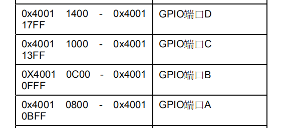
- Find the starting address of the GPIOX port
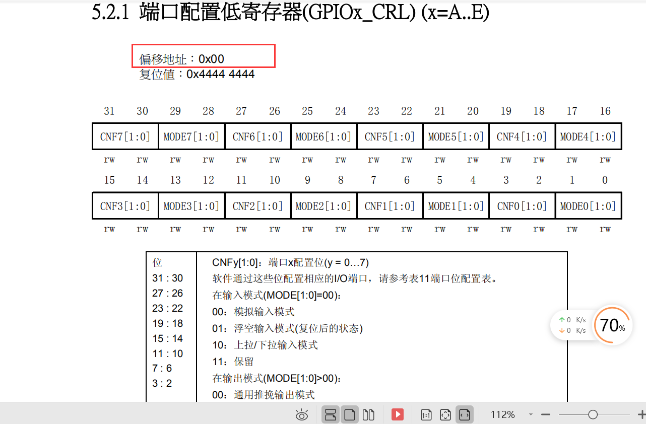
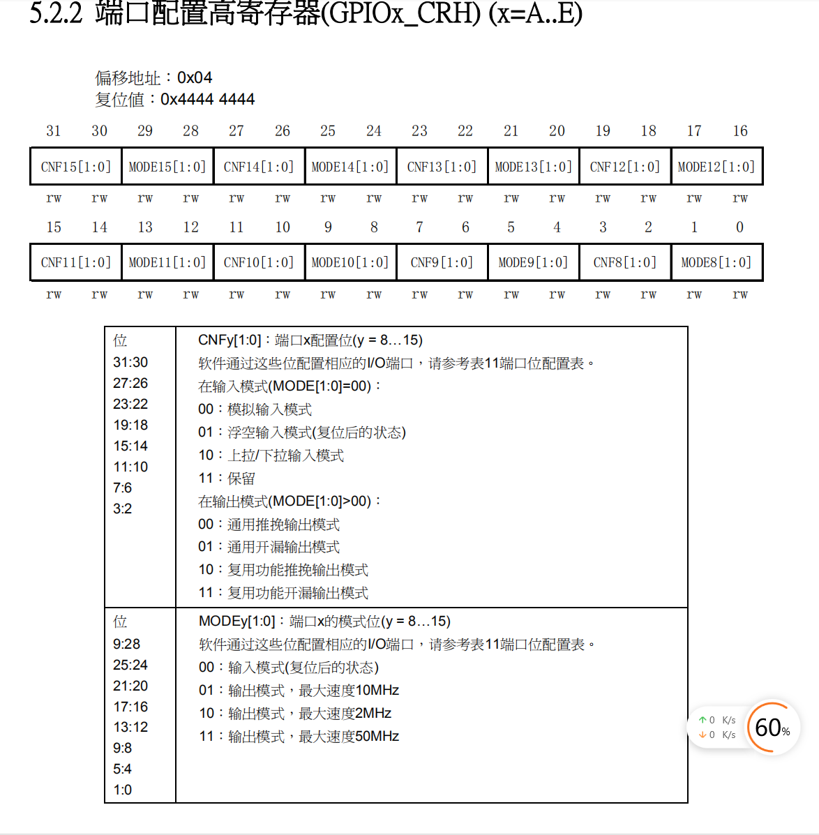
Because each io of STM32 needs 4 bits to be configured, a 32-bit register can only be configured with 8 IO at most (the register of 32-bit MCU is 32-bit). In STM32, use the port configuration low register (GPIOx_CRL) to configure pins Px0-Px7, and use the port configuration high register (GPIOx_CRH) to configure pins Px8-Px15.
The universal push-pull output mode is adopted in this test, and the maximum output clock frequency is 2Mhz. A12, B1 and C14 pins are used respectively. Among them, B1 belongs to port configuration, the low register offset address is 0x00, and C14 and A12 belong to port configuration, and the high register offset address is 0x04.
- Locate the port configuration low register (GPIOx_CRL) in the GPIO register Control port low eight bit IO
- Locate the port configuration high register (GPIOx_CRH) in the GPIO register to control the high octet IO of the port
- Register configuration
	//----------------GPIOA configuration register------------------------
#define GPIOA_CRH	*((unsigned volatile int*)0x40010804)
#define	GPIOA_ODR	*((unsigned volatile int*)0x4001080C)
//----------------GPIOB configuration register------------------------
#define GPIOB_CRL	*((unsigned volatile int*)0x40010C00)
#define	GPIOB_ODR	*((unsigned volatile int*)0x40010C0C)
//----------------GPIOC configuration register------------------------
#define GPIOC_CRH	*((unsigned volatile int*)0x40011004)
#define	GPIOC_ODR	*((unsigned volatile int*)0x4001100C)
- Output mode
    GPIOA_CRH&=0xFFF0FFFF;		//Set bit reset
	GPIOA_CRH|=0x00020000;		//PA12 push pull output

	GPIOB_CRL&=0xFFFFFF0F;		//Set bit reset
	GPIOB_CRL|=0x00000020;		//PB1 push pull output

	GPIOC_CRH&=0xF0FFFFFF;		//Set bit reset
	GPIOC_CRH|=0x02000000;   	//PC14 push pull output
(2) Enable clock
- Locate the clock enable register mapping base address
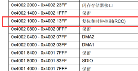
- Find the port offset address and the location of the corresponding port
//----------------APB2 enable clock register---------------------
#define RCC_AP2ENR	*((unsigned volatile int*)0x40021018)
    RCC_AP2ENR|=1<<2;			//APB2-GPIOA peripheral clock enable
	RCC_AP2ENR|=1<<3;			//APB2-GPIOB peripheral clock enable
	RCC_AP2ENR|=1<<4;			//APB2-GPIOC peripheral clock enable
2, Code
(1) main.c
#define RCC_AP2ENR	*((unsigned volatile int*)0x40021018)
	//----------------GPIOA configuration register------------------------
#define GPIOA_CRH	*((unsigned volatile int*)0x40010804)
#define	GPIOA_ORD	*((unsigned volatile int*)0x4001080C)
//----------------GPIOB configuration register------------------------
#define GPIOB_CRL	*((unsigned volatile int*)0x40010C00)
#define	GPIOB_ORD	*((unsigned volatile int*)0x40010C0C)
//----------------GPIOC configuration register------------------------
#define GPIOC_CRH	*((unsigned volatile int*)0x40011004)
#define	GPIOC_ORD	*((unsigned volatile int*)0x4001100C)
//-------------------Simple delay function-----------------------
void  Delay_ms( volatile  unsigned  int  t)
{
     unsigned  int  i;
     while(t--)
         for (i=0;i<800;i++);
}
//------------------------Main function--------------------------
int main()
{
	int j=100;
	RCC_AP2ENR|=1<<2;			//APB2-GPIOA peripheral clock enable
	RCC_AP2ENR|=1<<3;			//APB2-GPIOB peripheral clock enable
	RCC_AP2ENR|=1<<4;			//APB2-GPIOC peripheral clock enable
	//These two lines of code can be combined into RCC_ APB2ENR|=1<<3|1<<4;
	GPIOA_CRH&=0xFFF0FFFF;		//Set bit reset
	GPIOA_CRH|=0x00020000;		//PA12 push pull output
	GPIOA_ORD|=1<<12;			//Set the initial light to on

	GPIOB_CRL&=0xFFFFFF0F;		//Set bit reset
	GPIOB_CRL|=0x00000020;		//PB1 push pull output
	GPIOB_ORD|=1<<1;			//Set the initial light to off

	GPIOC_CRH&=0xF0FFFFFF;		//Set bit reset
	GPIOC_CRH|=0x02000000;   	//PC14 push pull output
	GPIOC_ORD|=1<<14;			//Set the initial light to off
	while(j)
	{
		GPIOA_ORD=0x1<<12;		//PA12 high level
		Delay_ms(3000000);
		GPIOA_ORD=0x0<<12;		//PA12 low level
		Delay_ms(3000000);

		GPIOB_ORD=0x1<<1;		//PB1 high level
		Delay_ms(3000000);
		GPIOB_ORD=0x0<<1;		//PB1 low level
		Delay_ms(3000000);

		GPIOC_ORD=0x1<<14;		//PC14 high level
		Delay_ms(3000000);
		GPIOC_ORD=0x0<<14;		//PC14 low level
		Delay_ms(3000000);
	}
}
(2) Wiring:
- GND of USB to TTL module is connected to the ground of the smallest system board
- 3v3 of USB to TTL module connected to the minimum system board 3v3
- TXD of USB to TTL module is connected to PA10 of the smallest system board
- RXD of USB to TTL module is connected to PA9 of the smallest system board
- PA12, PB1 and PC14 of the smallest system board are respectively connected to the positive pole of red, yellow and green LED lamps, and the negative pole of LED lamps is grounded.
As shown in the figure:
You should pay attention to downloading hex files
There are many ways to download different combinations of BOOT0 and BOOT1 pins
| BOOT1=x | BOOT0=0 | Boot from user flash, this is the normal operating mode. |
| BOOT1=0 | BOOT0=1 | (ISP mode) start from the system memory. The program function started in this mode is set by the manufacturer. |
| BOOT1=1 | BOOT0=1 | Starting from the built - in SRAM, this mode can be used for debugging |
3, Burning program
4, Experimental results
reference resources: stm32 fancy point water lamp_ Xinghe blog - CSDN blog
Based on assembly and C language, STM32 water lamp flashes in turn_ Laul Ken Yi's blog - CSDN blog
stm32 from address to register_ Geekyatao CSDN blog_ stm32 register address