STM32 timer input capture
STM32F429 is used as a timer to capture the PWM waveform, and the cycle, frequency, duty cycle and forward pulse width of the waveform are measured.
Basic principles
The input acquisition of timer is mainly to measure the frequency, pulse width, duty cycle and other information of input signal.
You need to understand the basic structure of stm32 timer
The main understanding of these frames is the key point. They are all my own understanding. I have little talent and learning. If I have a wrong understanding, I hope to correct it.
As for the first half of the clock, it is not too difficult to understand. The following channels are complex in understanding.
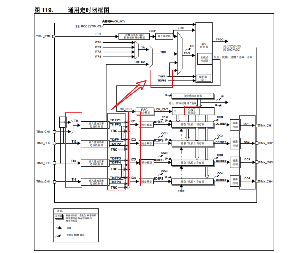
Firstly, a general timer has four input channels and four channels, which can be empty or reused to the corresponding GPIO,
/*
 	Can output to GPIO of TIM passageway:

	TIM1_CH1, PA8,	PE9,
	TIM1_CH2, PA9,	PE11
	TIM1_CH3, PA10,	PE13
	TIM1_CH4, PA11,	PE14

	TIM2_CH1, PA15 (429439 only) 407 No such foot
	TIM2_CH2, PA1,	PB3
	TIM2_CH3, PA2,	PB10
	TIM2_CH4, PA3,	PB11

	TIM3_CH1, PA6,  PB4, PC6
	TIM3_CH2, PA7,	PB5, PC7
	TIM3_CH3, PB0,	PC8
	TIM3_CH4, PB1,	PC9

	TIM4_CH1, PB6,  PD12
	TIM4_CH2, PB7,	PD13
	TIM4_CH3, PB8,	PD14
	TIM4_CH4, PB9,	PD15

	TIM5_CH1, PA0,  PH10
	TIM5_CH2, PA1,	PH11
	TIM5_CH3, PA2,	PH12
	TIM5_CH4, PA3,	PI10

	TIM8_CH1, PC6,  PI5
	TIM8_CH2, PC7,	PI6
	TIM8_CH3, PC8,	PI7
	TIM8_CH4, PC9,	PI2

	TIM9_CH1, PA2,  PE5
	TIM9_CH2, PA3,	PE6

	TIM10_CH1, PB8,  PF6

	TIM11_CH1, PB9,  PF7

	TIM12_CH1, PB14,  PH6
	TIM12_CH2, PB15,  PH9

	TIM13_CH1, PA6,  PF8
	TIM14_CH1, PA7,  PF9
However, a channel can only be configured into one mode. For example, if it is configured into output mode, it cannot be configured into input mode. Although a channel has several gpios that can be set, after setting one other channel, it cannot be set in this channel.
Because you want to capture the input signal, set it to the input mode. The key is the channel relationship on the left side of the figure
TI1 to TI4 represent four input channels, but the input channel is not directly connected with the timer channel. After passing through the input filter and edge detector, an input channel is divided into two and can be sent to two timer channels respectively, such as TI1FP1 and TI1FP2. These are separated from the first input channel and can be sent to IC1 and IC2 respectively, IC means the input channel, so that the capture channel of the rear timer can capture a rising edge and a falling edge, so that the frequency and duty cycle of one PWM can be measured.
The next important issue is the clock speed of each timer.
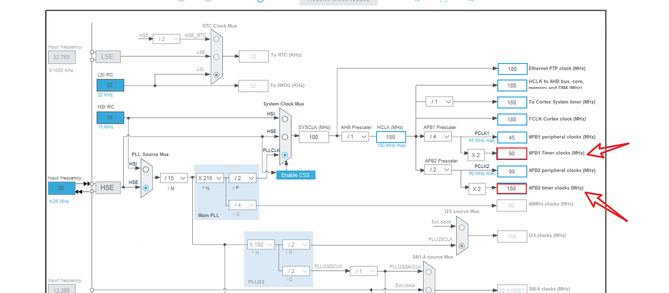
It can be seen from the clock tree that the clock speeds of timers on APB1 and APB2 are different.
	APB1 Timer yes TIM2, TIM3 ,TIM4, TIM5, TIM6, TIM7, TIM12, TIM13, TIM14
	APB2 Timer yes TIM1, TIM8 ,TIM9, TIM10, TIM11


	APB1 Input clock of timer TIMxCLK = SystemCoreClock / 2; 90M
	APB2 Input clock of timer TIMxCLK = SystemCoreClock; 180M
Therefore, pay attention to the frequency of the timer when configuring the frequency division coefficient of the timer and finally calculating the signal frequency.
The principle of calculating the frequency and duty cycle of the input acquisition signal is as follows:
Assuming that the counting direction of the counter is upward, the timer will accumulate upward according to the speed after frequency division. When the set edge is encountered, the current counting value will be saved. By reading this value, we can know when the edge is detected. Through the difference of different edge times, we can calculate the frequency and other information.
code
Generate code using Cubemx
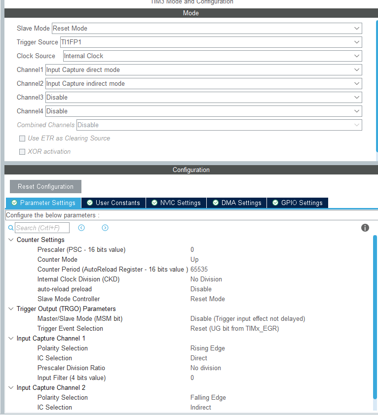
This timer is configured to detect PWM signals.
The first two options, slave mode, are used to configure TI1FP1 trigger, and the result after trigger is reset. The key to this setting is the implementation principle of the later code. This setting means that after TI1FP1 trigger, the whole counter will be reset, counting from 0. If such a filter and frequency divider are not set in front, TI1FP1 is the first input signal, For example, after the level trigger is set, once the high level comes, all the previous reset starts timing, which is like when the high level of PWM signal comes, all reset, and then the first timer channel starts timing. The value will not be recorded until it meets the next rising edge, and the second timer channel also starts timing at the same time, The value is not recorded until the falling edge is encountered. It is not difficult to find that the value recorded in the first channel is the value of the whole cycle, while the value recorded in the second channel is the value from the rising edge to the falling edge, which is the value of PWM forward pulse width. In this way, the desired result is obtained, so it is necessary to set this mode.
The following two options are the choice of two channels of the timer. Back to the structural block diagram, there are two choices for the input of channel 1, TI1FP1 and TI2FP1. The first choice is direct connection, the second choice is non direct connection, and the choice of the second way is the same. The hardware configuration is GPIO of channel 1, so channel 1 is directly connected and channel 2 is not directly connected.
The following configurations are quite clear. In the parameter selection below, a rising edge is triggered and a falling edge is triggered.
The following mainly involves three functions:
TIM_HandleTypeDef htim3;
__IO uint16_t IC2Value = 0;
__IO uint16_t IC1Value = 0;
__IO float DutyCycle = 0;
__IO float Frequency = 0;


void bsp_SetPWMCapture()
{
	  /* USER CODE BEGIN TIM3_Init 0 */

  /* USER CODE END TIM3_Init 0 */

  TIM_ClockConfigTypeDef sClockSourceConfig = {0};
  TIM_SlaveConfigTypeDef sSlaveConfig = {0};
  TIM_MasterConfigTypeDef sMasterConfig = {0};
  TIM_IC_InitTypeDef sConfigIC = {0};
/*
Above are three handle structures

 */
  /* USER CODE BEGIN TIM3_Init 1 */

  /* USER CODE END TIM3_Init 1 */
  htim3.Instance = TIM3;
  htim3.Init.Prescaler = 90-1;
  htim3.Init.CounterMode = TIM_COUNTERMODE_UP;
  htim3.Init.Period = 65535;
  htim3.Init.ClockDivision = TIM_CLOCKDIVISION_DIV1;
  htim3.Init.AutoReloadPreload = TIM_AUTORELOAD_PRELOAD_DISABLE;
  /*
Some frequency division coefficients are mainly set above

 */
  if (HAL_TIM_Base_Init(&htim3) != HAL_OK)
  {
    Error_Handler(__FILE__, __LINE__);
  }
  sClockSourceConfig.ClockSource = TIM_CLOCKSOURCE_INTERNAL;
  if (HAL_TIM_ConfigClockSource(&htim3, &sClockSourceConfig) != HAL_OK)
  {
    Error_Handler(__FILE__, __LINE__);
  }
  if (HAL_TIM_IC_Init(&htim3) != HAL_OK)
  {
    Error_Handler(__FILE__, __LINE__);
  }
  sSlaveConfig.SlaveMode = TIM_SLAVEMODE_RESET;
  sSlaveConfig.InputTrigger = TIM_TS_TI1FP1;
  sSlaveConfig.TriggerPolarity = TIM_INPUTCHANNELPOLARITY_RISING;
  sSlaveConfig.TriggerFilter = 0;
  /*
The slave mode is set above. For example, when it is set to reset mode, TI1FP1 rising edge is triggered

 */
  if (HAL_TIM_SlaveConfigSynchro(&htim3, &sSlaveConfig) != HAL_OK)
  {
    Error_Handler(__FILE__, __LINE__);
  }
  sMasterConfig.MasterOutputTrigger = TIM_TRGO_RESET;
  sMasterConfig.MasterSlaveMode = TIM_MASTERSLAVEMODE_DISABLE;
/*
The above is not used for input capture

 */
  if (HAL_TIMEx_MasterConfigSynchronization(&htim3, &sMasterConfig) != HAL_OK)
  {
    Error_Handler(__FILE__, __LINE__);
  }
  sConfigIC.ICPolarity = TIM_INPUTCHANNELPOLARITY_RISING;
  sConfigIC.ICSelection = TIM_ICSELECTION_DIRECTTI;
  sConfigIC.ICPrescaler = TIM_ICPSC_DIV1;
  sConfigIC.ICFilter = 0;
  /*
The above is the configuration parameters of channel 1

 */
  if (HAL_TIM_IC_ConfigChannel(&htim3, &sConfigIC, TIM_CHANNEL_1) != HAL_OK)
  {
    Error_Handler(__FILE__, __LINE__);
  }
  sConfigIC.ICPolarity = TIM_INPUTCHANNELPOLARITY_FALLING;
  sConfigIC.ICSelection = TIM_ICSELECTION_INDIRECTTI;
/*
The above is the configuration parameters of channel 2

 */
  if (HAL_TIM_IC_ConfigChannel(&htim3, &sConfigIC, TIM_CHANNEL_2) != HAL_OK)
  {
    Error_Handler(__FILE__, __LINE__);
  }
  /* USER CODE BEGIN TIM3_Init 2 */
	HAL_TIM_IC_Start_IT(&htim3,TIM_CHANNEL_1);
	HAL_TIM_IC_Start_IT(&htim3,TIM_CHANNEL_2);
	/*
The above is to enable the input capture interrupt of two channels. cubemx will not automatically generate these two sentences and needs to add them manually

 */
  /* USER CODE END TIM3_Init 2 */

}
/*
HAL_TIM_Base_MspInit It is a weakly defined function of HAL library. After it is defined here, it will be subject to this definition
HAL_TIM_Base_Init This function will be called to initialize GPIO and interrupt parameters.
 */
void HAL_TIM_Base_MspInit(TIM_HandleTypeDef* tim_baseHandle)
{

  GPIO_InitTypeDef GPIO_InitStruct = {0};
  if(tim_baseHandle->Instance==TIM1)
  {

  }
  else if(tim_baseHandle->Instance==TIM2)
  {

  }
  else if(tim_baseHandle->Instance==TIM3)
  {
  /* USER CODE BEGIN TIM3_MspInit 0 */

  /* USER CODE END TIM3_MspInit 0 */
    /* TIM3 clock enable */
    __HAL_RCC_TIM3_CLK_ENABLE();

    __HAL_RCC_GPIOC_CLK_ENABLE();
    /**TIM3 GPIO Configuration
    PC6     ------> TIM3_CH1
    */
    GPIO_InitStruct.Pin = GPIO_PIN_6;
    GPIO_InitStruct.Mode = GPIO_MODE_AF_PP;
    GPIO_InitStruct.Pull = GPIO_NOPULL;
    GPIO_InitStruct.Speed = GPIO_SPEED_FREQ_LOW;
    GPIO_InitStruct.Alternate = GPIO_AF2_TIM3;
    HAL_GPIO_Init(GPIOC, &GPIO_InitStruct);

    /* TIM3 interrupt Init */
    HAL_NVIC_SetPriority(TIM3_IRQn, 0, 0);
    HAL_NVIC_EnableIRQ(TIM3_IRQn);
  /* USER CODE BEGIN TIM3_MspInit 1 */

  /* USER CODE END TIM3_MspInit 1 */
  }

}
/*
//__HAL_TIM_SET_CAPTUREPOLARITY(__HANDLE__, __CHANNEL__, __POLARITY__)You can set the input trigger edge of the specified timer and channel
 The next step is to interrupt the service function. If the input capture is interrupted, the callback function will be invoked in the interrupt service function of the HAL library.
*/

void HAL_TIM_IC_CaptureCallback(TIM_HandleTypeDef *htim)
{
	if(TIM3 == htim->Instance)
	{
		if (htim->Channel == HAL_TIM_ACTIVE_CHANNEL_1)
		{
			/* Get input capture value */
			IC1Value = HAL_TIM_ReadCapturedValue(&htim3,TIM_CHANNEL_1);
			IC2Value = HAL_TIM_ReadCapturedValue(&htim3,TIM_CHANNEL_2);
			if (IC1Value != 0)
			{
				/* Duty cycle calculation */
				DutyCycle = (float)((IC2Value+1) * 100) / (IC1Value+1);

				/* Frequency calculation */
				Frequency = 90000000/90/(float)(IC1Value+1);

			}
			else
			{
				DutyCycle = 0;
				Frequency = 0;
			}

		}
	}
}
In addition, you need to define a large interrupt service function.
void TIM3_IRQHandler(void)
{
  /* USER CODE BEGIN TIM3_IRQn 0 */

  /* USER CODE END TIM3_IRQn 0 */
  HAL_TIM_IRQHandler(&htim3);//In this function, the above customized service function will be called back
  /* USER CODE BEGIN TIM3_IRQn 1 */

  /* USER CODE END TIM3_IRQn 1 */
}
So far, the configuration is completed, and the initialization is done in the main function. After generating the PWM wave, connect the output pin and the input pin to get the waveform data.
Firstly, a PWM wave with 2k frequency and 30 duty cycle is set. The following are the experimental results:
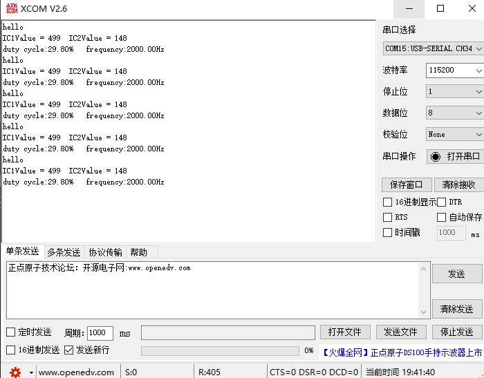
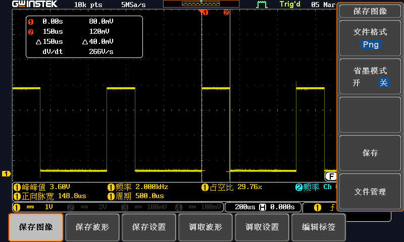
It is completely consistent with the data measured by oscilloscope.
If there are any errors or deficiencies in this article, please correct them.