1, Introduction to TFT-LCD
TFT-LCD (thin film transistor liquid crystal display) is a thin film transistor liquid crystal display. TFT-LCD is different from the simple matrix of passive TN-LCD and STN-LCD. It is equipped with a thin film transistor (TFT) on each pixel of the LCD, which can effectively overcome the crosstalk when it is not gated, and make the static characteristics of the LCD independent of the number of scanning lines, so it greatly improves the image quality. TFT-LCD is also called true color LCD.
Although TFT-LCD is collectively referred to as LCD However, it is an active matrix LCD, which is used in television Flat panel display and Projector Come on.
1.1 detection principle of resistive touch screen
The resistive touch screen structure is shown below. It is mainly composed of surface hard coating, two ITO layers, spacing points and glass bottom layer. These structural layers are transparent. The whole touch screen is covered on the liquid crystal panel, and the liquid crystal panel can be seen through the touch screen. The surface coating plays a protective role, and the glass bottom layer plays a bearing role. The two ITO layers are the key structure of the touch screen. They are the conductive layer coated with indium tin metal oxide. A spacing point is used between the two ITO layers to separate the two layers. When the surface of the touch screen is under pressure, the surface bends to make the upper ITO contact with the lower ITO, and the circuit is connected at the contact.
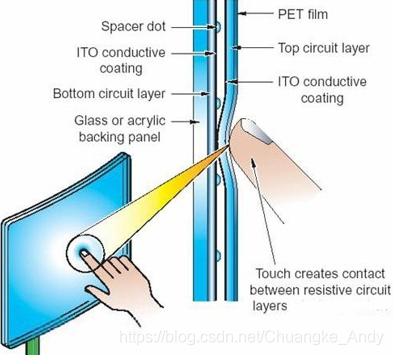
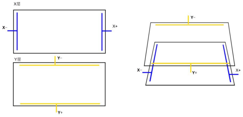
Four electrodes X -, x +, Y - and y + are respectively led out from both ends of the two ITO coatings, which is the most common four wire structure of the resistance screen. Through these electrodes, the external circuit can apply a uniform electric field or detection voltage to the two coatings.
When the touch screen is pressed, the two ITO layers contact each other, and the ITO layer is divided into two resistors from the contact. Because the ITO layer is uniformly conductive, the size of the two resistors is proportional to the distance between the contact and the two electrodes. Using this feature, the coordinates can be detected through the following process, which is the origin of the name of the resistive touch screen.
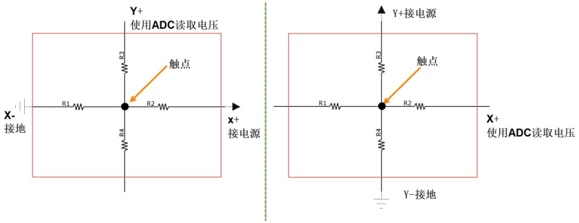
- When calculating the X coordinate, the driving voltage Vref is applied to the X + electrode, and the X-electrode is grounded, so a uniform electric field is formed at x + and X -, and the voltage at the contact is collected through the Y + electrode. Because the ITO layer is uniformly conductive, the ratio of contact voltage to VREF is equal to the ratio of contact X coordinate to screen width, so:
x = V Y V r e f × W i d t h x = \frac{V_{Y}}{V_{ref}} \times Width x=VrefVY×Width - When calculating the Y coordinate, the driving voltage Vref is applied to the y + electrode, and the Y-electrode is grounded, so a uniform electric field is formed at y + and Y -, and the voltage at the contact is collected through the X + electrode. Because the ITO layer is uniformly conductive, the ratio of contact voltage to VREF is equal to the ratio of contact y coordinate to screen height, so:
y = V Y V r e f × H e i g h t y = \frac{V_{Y}}{V_{ref}} \times Height y=VrefVY×Height
1.2 introduction to xpt2046 resistive touch screen controller
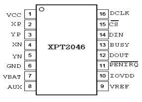
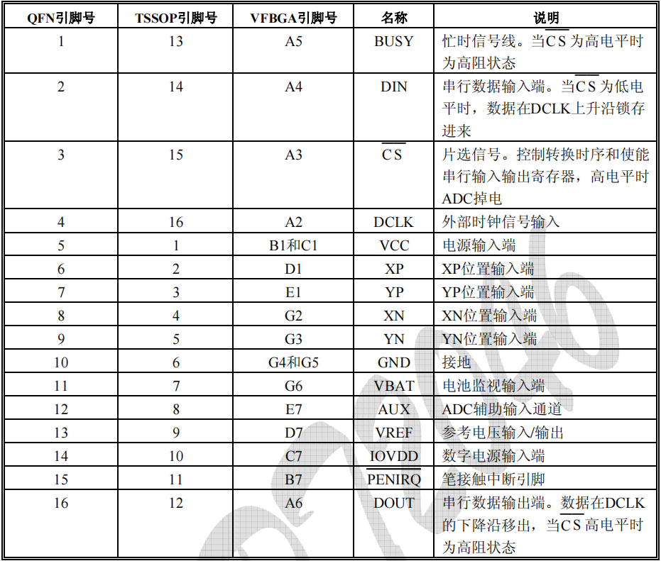
In order to facilitate the detection of touch coordinates, some chip manufacturers have made special control chips for resistance screen to control the above acquisition process and acquisition voltage. The external microcontroller directly communicates with the touch control chip to directly obtain the contact voltage or coordinates. Wildfire 3.2-inch resistive touch screen uses XPT2046 chip as the touch control chip. XPT2046 chip controls the 4-wire resistive touch screen, uses SPI mode for communication, and contains a 12 bit resolution 125KHz conversion rate gradually approaching A/D converter. XPT2046 pin diagram (TSSOP-16 package) and pin description are shown as follows:
2, Introduction to FSMC
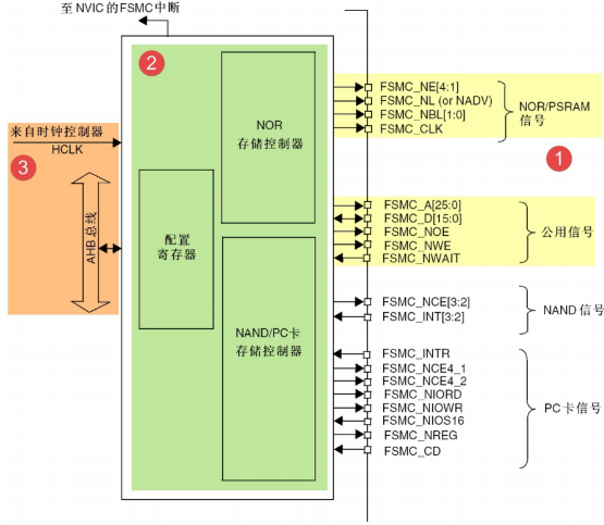
FSMC (Flexible Static Memory Controller) is translated into flexible static storage controller. STM32F1 series chips use FSMC peripherals to manage extended memory. It can be used to drive SRAM, NOR FLASH and NAND FLSAH memory, but can not drive dynamic memory such as SDRAM. In STM32F429 series controllers, it has FMC peripherals to support the control of SDRAM memory.
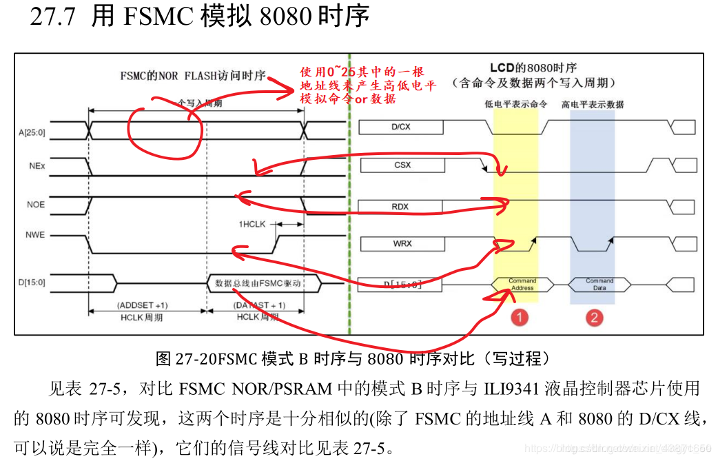
Because FSMC peripherals can be used to control the extended external memory, the operation of MCU on LCD screen is actually to write the display data into the display memory, which is very similar to the control memory, and the communication sequence of 8080 interface can be generated by FSMC peripherals, so it is very suitable to use FSMC to control LCD screen.
3, Pin determination
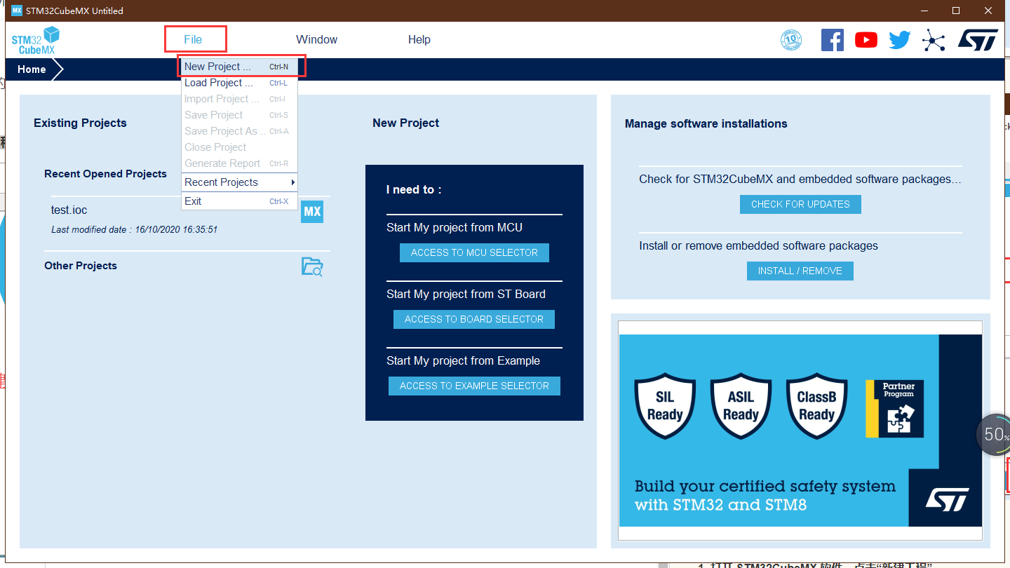
4, New project
1. Open STM32CubeMX software and click "new project"
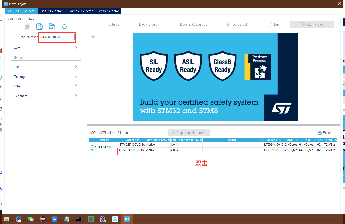
2. Select MCU and package
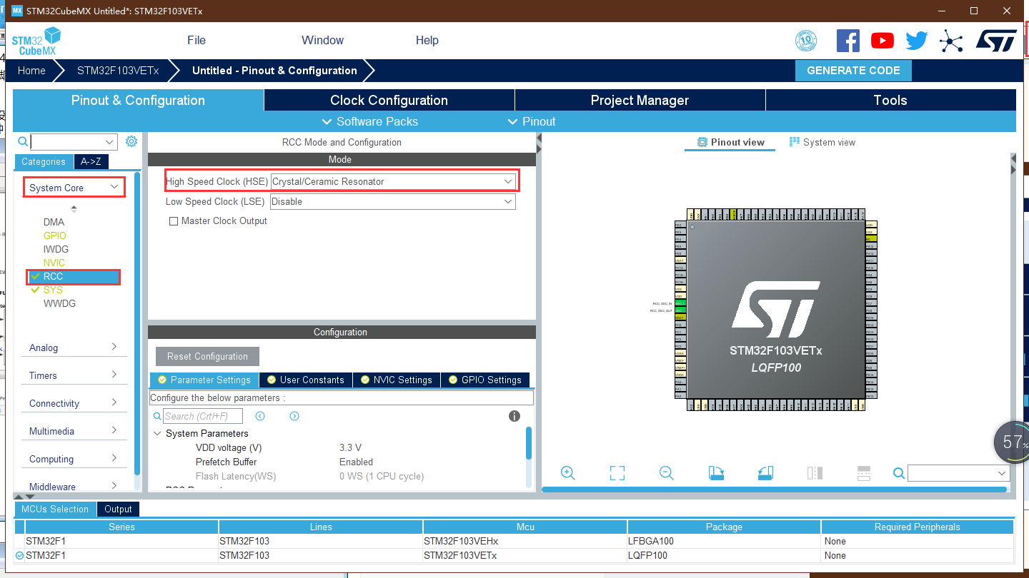
3. Configure clock
RCC setting, select HSE as crystal / ceramic resonator
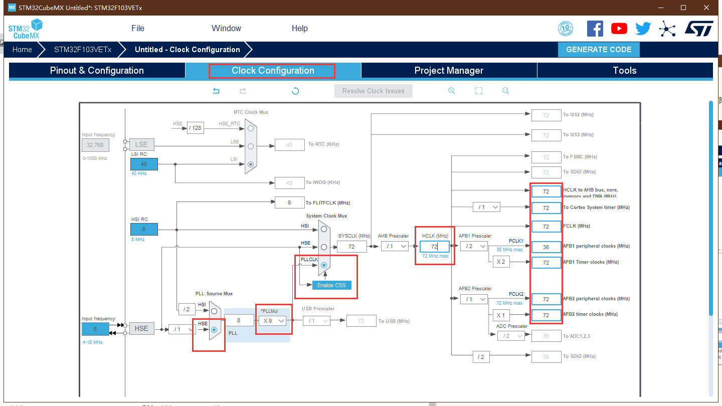
Select Clock Configuration to configure the system clock SYSCLK to 72MHz
After modifying the value of HCLK to 72, enter enter, and the software will automatically modify all configurations
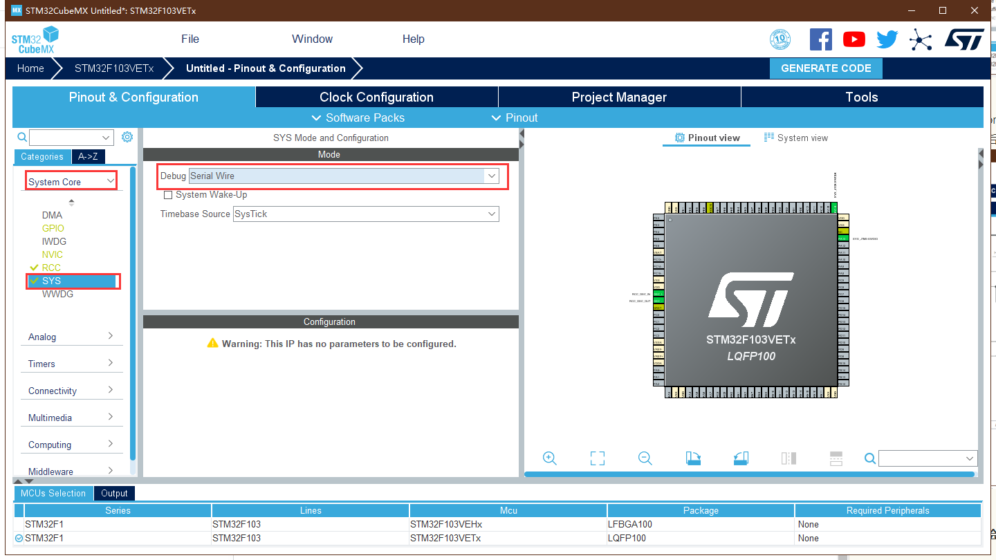
4. Configure debugging mode
A very important step, otherwise the debugger will not be recognized after the first burning of the program
SYS setting, select Debug as Serial Wire
5, FSMC
5.1 parameter configuration
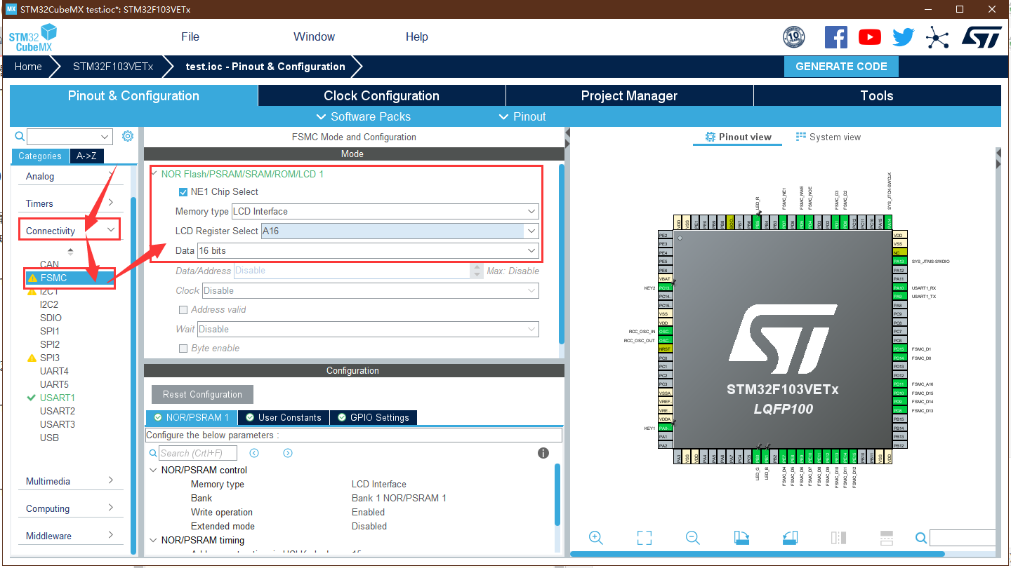
Select FSMC setting in Connectivity, and select NE1 Chip Select in NOR Flash/PSRAM/SRAM/ROM/LCD 1. Select the chip selection pin NE1 in the schematic diagram [select the first area of Bank1 according to the mapping pin of the schematic diagram, and the pins corresponding to different areas are different]
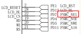
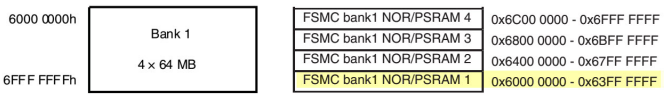
FSMC_NE is a chip selection control signal line for controlling the memory chip, and STM32 has FSMC_NE1/2/3/4 pins. Different pins correspond to different address areas in STM32. For example, when STM32 accesses 0x68000000-0x6bfffffff address space, FSMC_NE3 pin will be automatically set to low level. Since it is generally connected to the chip selection pin of external memory and the low level is valid, the chip selection of external memory is enabled and 0x6000000 is accessed-
0x63FFFFFF address, FSMC_NE1 will output low level. When using different FSMC_ When the ne pin is connected to the external memory, the address of STM32 accessing the external memory is different, so as to control multiple external memory chips.
- Memory type: select LCD interface
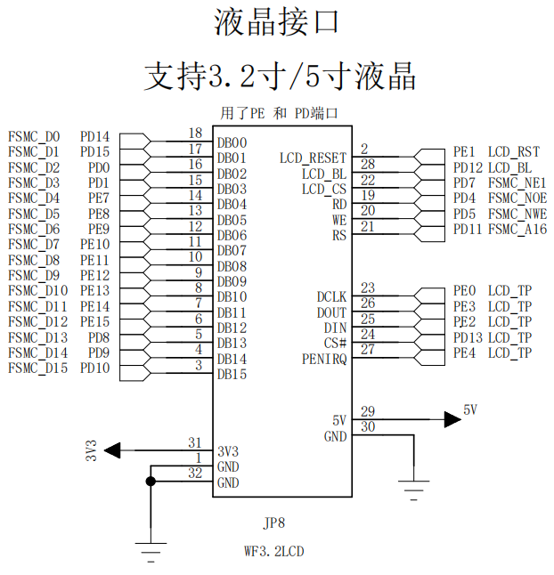
- LCD Register Select (RS pin): select A16. The RS pin is the command / data selection bit. It is also known from the schematic diagram that A16 should be selected here
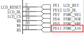
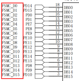
- Data (set the data width of the memory to be controlled): select 16 bits. It is obvious from the schematic diagram that there are 16 data pins. Just select 16 bits here
Configure specific parameters in NOR/PSRAM 1.
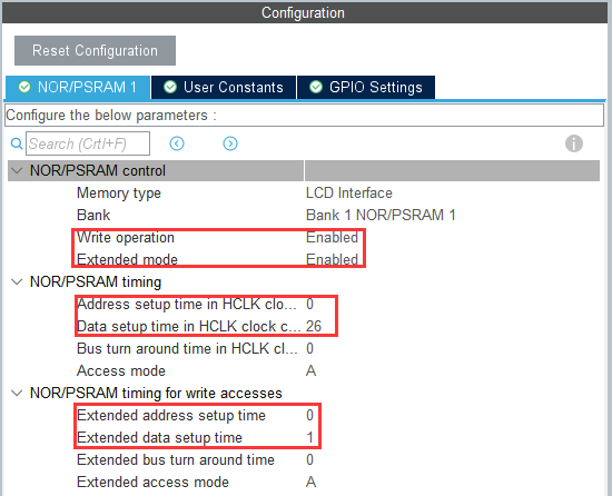
NOR/PSRAM control:
- Write operation: select Enabled. If write is disabled, FSMC can only read data from the memory and cannot write.
- Extended mode: select Enabled. In the non extended mode, only FSMC is used for memory read / write timing_ Configuration in BCR register; In the extended mode, the read-write timing of the memory can be configured separately, and the read timing uses FSMC_BCR register, write timing using FSMC_BWTR register configuration.
5.1.1 FSMC read timing configuration
A basic concept is introduced here:
HCLK cycle:
According to the default configuration of STM32F103, the clock frequency of HCLK is 72MHz, that is, a THCLK is 1/72us=0.0138us=13.8us.
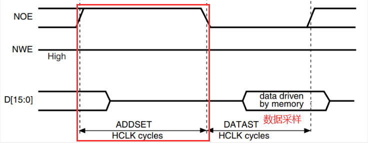
NOR/PSRAM timing (FSMC read timing configuration):
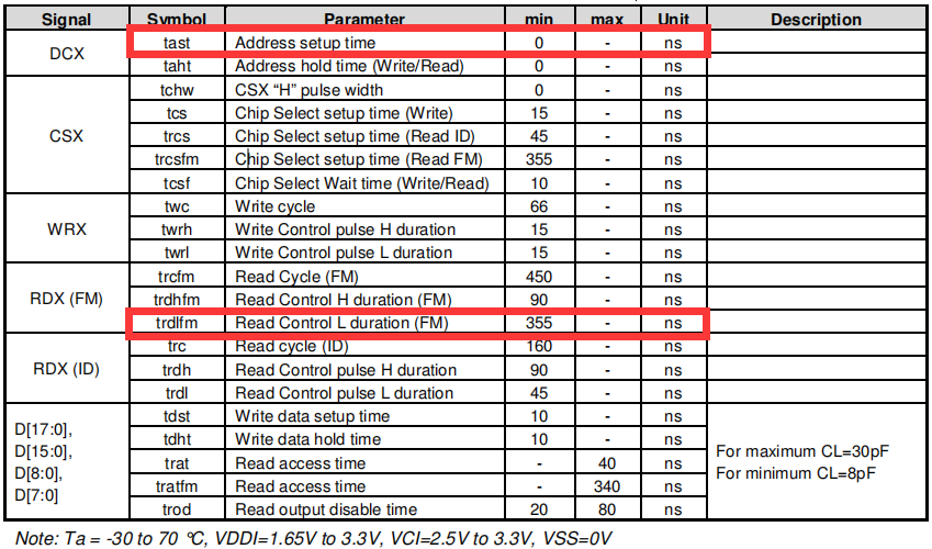
- Address setup time in HCLK clock cycles: Enter 0
- Data setup time in HCLK clock cycles: fill in 26
Configure FSMC read timing according to ILI9341 timing
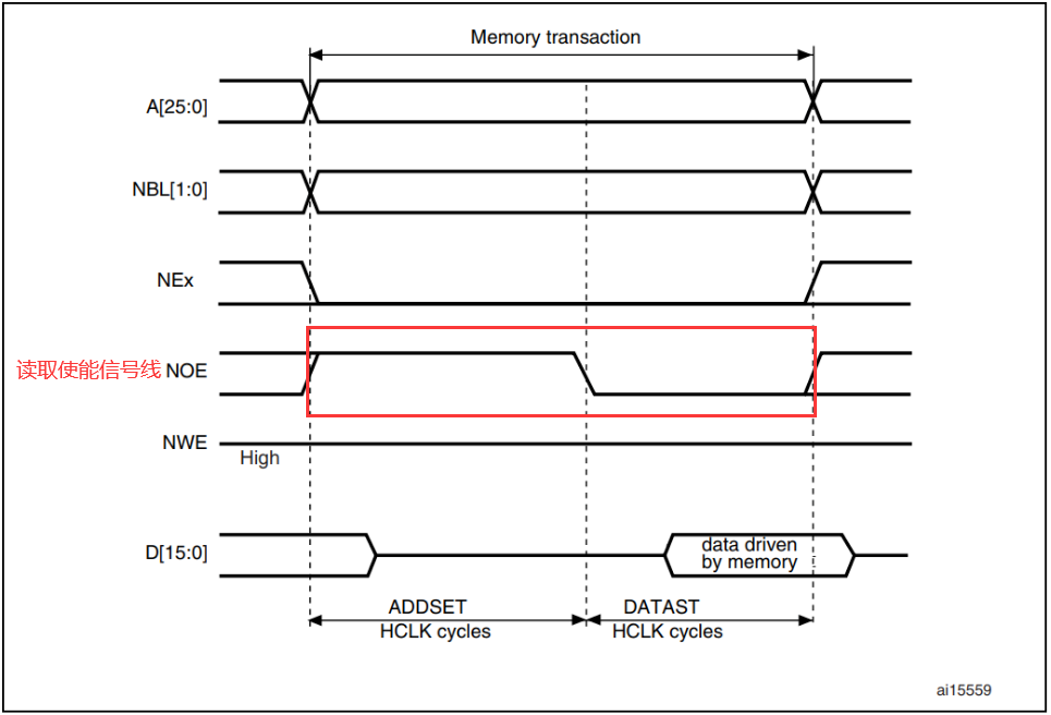
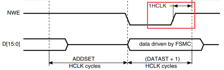
After NEx chip selection, NOE should maintain high level for a period of time, which is the ADDSET address establishment time (configurable through register FMC_BTRx).
Then NOE becomes low and read enable. The low level holding time is determined by the DATAST data establishment time (configurable through register FMC_BTRx).
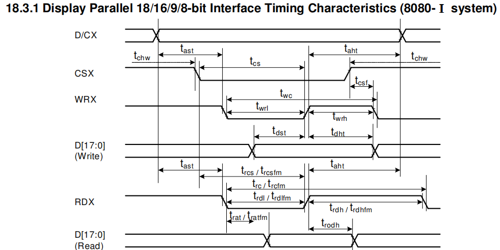
-
tast:
tast represents the address establishment time, with a minimum of 0ns
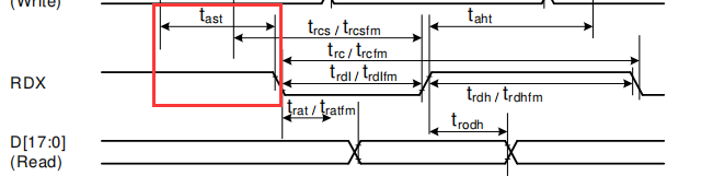
As can be seen from the timing chart, FSMC will sample data after the ADDSET cycle and after entering the DATAST cycle.

Therefore, we set the (ADDSET)HCLK time to be greater than or equal to the tast address establishment time.
(ADDSET) hclk > = 0ns, (0) · 13.8 = 0ns, so ADDSET can be set to 0 to ensure that the minimum tast address establishment time is met. -
trdlfm:
trdlfm indicates the time of reading data low level, with a minimum of 355ns
The sequence diagram of ILI9341 does not give the relevant information when ILI9341 operates the data line to transmit the read data. We'd better meet the minimum time of reading data low level.
Of course, if you don't do it, it will have little impact. As long as FSMC obtains all the data to be accessed in the data sampling of this cycle of DATAST.
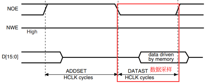
(DATAST)HCLK > 355ns, (26) * 13.8 = 358.8ns > 355ns, so DATAST is set to 26.
- Bus turn around time in HCLK clock cycles: fill in 0, which is only applicable to NOR Flash operation in bus reuse mode, so 0 is set here.
- Access mode: select A and the LCD controller uses Mode A, which is used to control SRAM/PSRAM and OE will flip. B mode is used when controlling asynchronous NOR FLASH.
5.1.2 FSMC write timing configuration
NOR/PSRAM timing for write accesses:
- Extended address setup time: 0
- Extended data setup time: fill in 1
Configure FSMC write timing according to ILI9341 timing
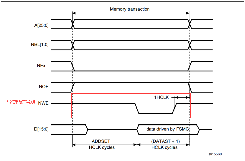
After NEx chip selection, NWE will maintain high level for a period of time, which is the ADDSET address establishment time (configurable through register FMC_BTRx).
After that, NWE becomes low and write is enabled. The time of low level holding is determined by the DATAST data establishment time (configurable through register FMC_BTRx).

-
tast:
tast represents the address establishment time, with a minimum of 0ns
It can be seen from the timing chart that FSMC will sample data after ADDSET cycle and DATAST cycle.
Therefore, we set the (ADDSET)HCLK time to be greater than or equal to the tast address establishment time.
(ADDSET) hclk > = 0ns, (0) · 13.8 = 0ns, so ADDSET can be set to 0 to ensure that the minimum tast address establishment time is met. -
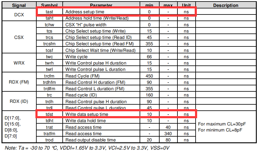
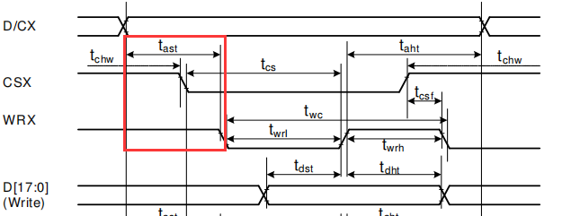
tdst,tdht:
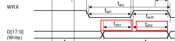
tdst: the minimum data setting time is 10ns. During this cycle, the WRX line is at the low level.
tdht: data holding time, which is the same as the minimum time of twrh write control high level, is 10ns. In this cycle, WRX line is at high level.
Observing the sequence diagram, we can set the tdst data setting time to 1HCLK (13.8 > 10) to meet the requirements of the minimum data setting time. We don't need to consider the tdht data holding time (see the sequence diagram of mode B above, after NWE becomes high level, it will last 1HCLK=13.8ns, which meets tdht by default).
Therefore, we only need to consider that the data establishment cycle DATAST should be greater than 10ns.
(DATAST) hclk > 10ns, 13.8 > 10, so DATAST is set to at least 1
- Extended bus turn around time: 0
- Extended access mode: select A
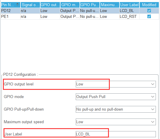
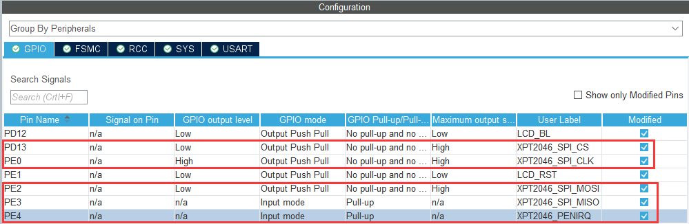
6, Setting backlight and reset pins
Select GPIO settings in System Core.
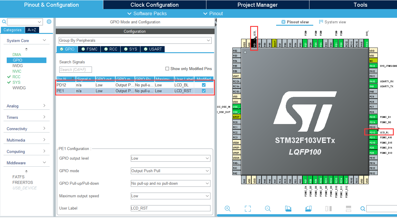
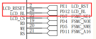
Find the corresponding pin of LCD backlight and reset in the figure on the right, and select GPIO_Output.
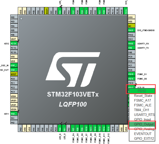
Select Low output level in GPIO output level to light up, and you can add a custom label (in this way, the generated code will also be defined according to the macro definition of the label setting pin).
7, Analog SPI
As these pins are drawn on the wildfire guide development board, analog SPI can only be used here. Hardware SPI interface can be used for actual projects.
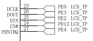
Select GPIO settings in System Core.
Configure the following 5 pins:
- XPT2046_SPI_CS
- XPT2046_SPI_CLK
- XPT2046_SPI_MOSI
- XPT2046_SPI_MISO
- XPT2046_SPI_PENIRQ pen contact interrupt pin
8, Generate code
Enter the project name and project path
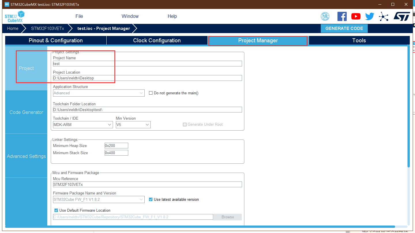
Select the IDE development environment MDK-ARM V5 for the application
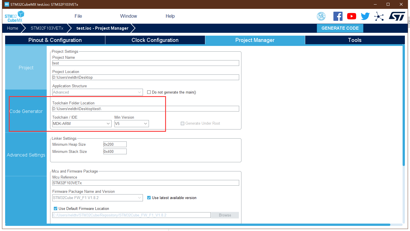
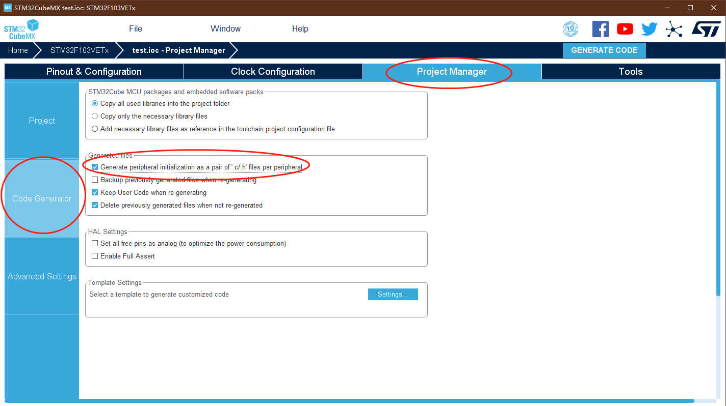
Each peripheral generates an independent ' c/.h 'document
Unchecked: all initialization codes are generated in main c
Check: the initialization code is generated in the corresponding peripheral file. For example, the GPIO initialization code is generated in GPIO C.
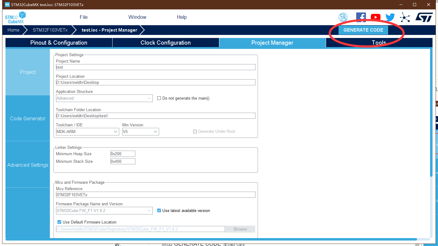
Click GENERATE CODE to generate the code
9, Modify code optimization level
The default optimization level of the code generated by STM32CubeMX is Level 3. Under this optimization level, the LCD screen cannot operate normally after it is compiled without error and downloaded to the development board; Adjust the optimization level to Level 0. After compiling and downloading, the LCD screen can operate normally and read the ID.
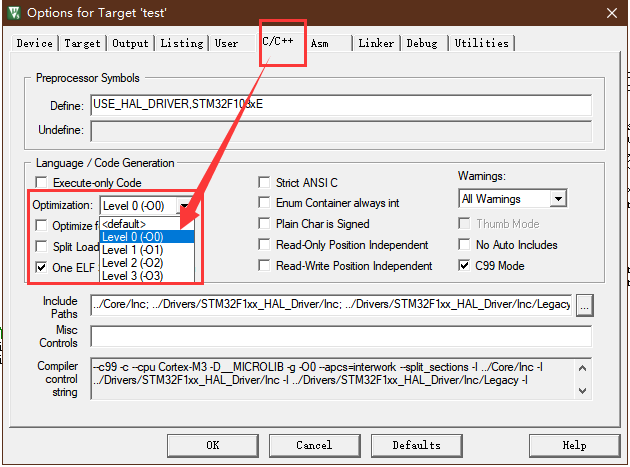
Introduction to C/C + + optimization level in KEIL5:
-O0: minimal optimization, which can cooperate to generate code debugging information to the greatest extent. It can break at any code line, especially at dead code.
-O1: limited optimization. Remove useless inline, useless static functions, dead code elimination, etc. and do not optimize where debugging information is affected. The most common optimization level in the code writing phase is to balance the appropriate code volume with sufficient debugging.
-O2: highly optimized, unfriendly debugging information, possible modification of code and function call execution process, automatic inlining of functions, etc.
-O3: optimize to the greatest extent and generate a very small amount of debugging information. There will be more code optimization, such as loop expansion, more radical function inlining, etc.
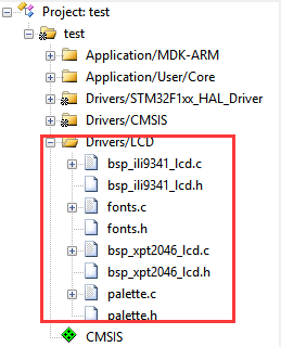
10, Add LCD driver file
Link: https://pan.baidu.com/s/1sNSlc5mRcfBRF6XgMkwXZA?pwd=kolq Extraction code: kolq
Add wild fire LCD display driver file to shield ili9341_ GPIO initialization ili9341 in init()_ GPIO_ Config() and FSMC configuration ILI9341_FSMC_Config(), mask XPT2046_Init(), because the STM32CubeMX project is in main C has been configured.
11, Modify main c
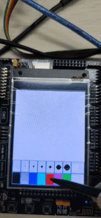
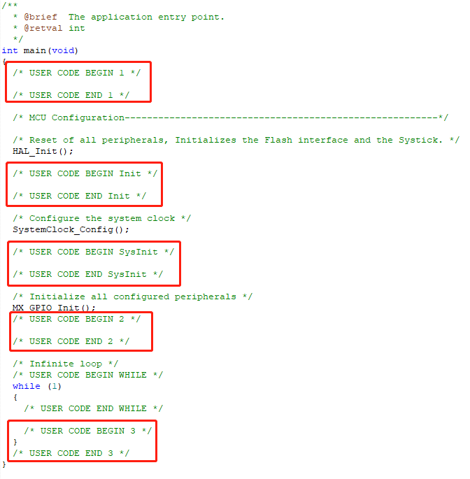
Join ili9341_ Init() after the LCD screen driver is initialized, start the Palette_Init() draws the touch pad interface, and then detects the touch xpt2046 in the while loop_ TouchEvenHandler().
/* USER CODE END Header */
/* Includes ------------------------------------------------------------------*/
#include "main.h"

/* Private includes ----------------------------------------------------------*/
/* USER CODE BEGIN Includes */
#include <stdio.h>
#include "bsp_ili9341_lcd.h"
#include "bsp_xpt2046_lcd.h"
#include "palette.h"
/* USER CODE END Includes */

/* Private typedef -----------------------------------------------------------*/
/* USER CODE BEGIN PTD */

/* USER CODE END PTD */

/* Private define ------------------------------------------------------------*/
/* USER CODE BEGIN PD */

/* USER CODE END PD */

/* Private macro -------------------------------------------------------------*/
/* USER CODE BEGIN PM */

/* USER CODE END PM */

/* Private variables ---------------------------------------------------------*/
UART_HandleTypeDef huart1;
DMA_HandleTypeDef hdma_usart1_rx;
DMA_HandleTypeDef hdma_usart1_tx;

SRAM_HandleTypeDef hsram1;

/* USER CODE BEGIN PV */

/* USER CODE END PV */

/* Private function prototypes -----------------------------------------------*/
void SystemClock_Config(void);
static void MX_GPIO_Init(void);
static void MX_DMA_Init(void);
static void MX_USART1_UART_Init(void);
static void MX_FSMC_Init(void);
/* USER CODE BEGIN PFP */

/* USER CODE END PFP */

/* Private user code ---------------------------------------------------------*/
/* USER CODE BEGIN 0 */

/* USER CODE END 0 */

/**
  * @brief  The application entry point.
  * @retval int
  */
int main(void)
{
  /* USER CODE BEGIN 1 */

  /* USER CODE END 1 */

  /* MCU Configuration--------------------------------------------------------*/

  /* Reset of all peripherals, Initializes the Flash interface and the Systick. */
  HAL_Init();

  /* USER CODE BEGIN Init */

  /* USER CODE END Init */

  /* Configure the system clock */
  SystemClock_Config();

  /* USER CODE BEGIN SysInit */

  /* USER CODE END SysInit */

  /* Initialize all configured peripherals */
  MX_GPIO_Init();
  MX_DMA_Init();
  MX_USART1_UART_Init();
  MX_FSMC_Init();
  /* USER CODE BEGIN 2 */
  ILI9341_Init();

  //Modes 0, 3, 5 and 6 are suitable for displaying text from left to right,
  //It is not recommended to use other modes to display text 	 The text displayed in other modes will have a mirror effect
  //Mode 6 is the default display direction for most LCD routines
  ILI9341_GramScan(3);
  //Draw touch pad interface
  Palette_Init(LCD_SCAN_MODE);
  /* USER CODE END 2 */

  /* Infinite loop */
  /* USER CODE BEGIN WHILE */
  while (1)
  {
    //Touch the detection function, which is called at least once in 10ms
    XPT2046_TouchEvenHandler();
    /* USER CODE END WHILE */

    /* USER CODE BEGIN 3 */
  }
  /* USER CODE END 3 */
}

/**
  * @brief System Clock Configuration
  * @retval None
  */
void SystemClock_Config(void)
{
  RCC_OscInitTypeDef RCC_OscInitStruct = {0};
  RCC_ClkInitTypeDef RCC_ClkInitStruct = {0};

  /** Initializes the RCC Oscillators according to the specified parameters
  * in the RCC_OscInitTypeDef structure.
  */
  RCC_OscInitStruct.OscillatorType = RCC_OSCILLATORTYPE_HSE;
  RCC_OscInitStruct.HSEState = RCC_HSE_ON;
  RCC_OscInitStruct.HSEPredivValue = RCC_HSE_PREDIV_DIV1;
  RCC_OscInitStruct.HSIState = RCC_HSI_ON;
  RCC_OscInitStruct.PLL.PLLState = RCC_PLL_ON;
  RCC_OscInitStruct.PLL.PLLSource = RCC_PLLSOURCE_HSE;
  RCC_OscInitStruct.PLL.PLLMUL = RCC_PLL_MUL9;
  if (HAL_RCC_OscConfig(&RCC_OscInitStruct) != HAL_OK)
  {
    Error_Handler();
  }
  /** Initializes the CPU, AHB and APB buses clocks
  */
  RCC_ClkInitStruct.ClockType = RCC_CLOCKTYPE_HCLK|RCC_CLOCKTYPE_SYSCLK
                              |RCC_CLOCKTYPE_PCLK1|RCC_CLOCKTYPE_PCLK2;
  RCC_ClkInitStruct.SYSCLKSource = RCC_SYSCLKSOURCE_PLLCLK;
  RCC_ClkInitStruct.AHBCLKDivider = RCC_SYSCLK_DIV1;
  RCC_ClkInitStruct.APB1CLKDivider = RCC_HCLK_DIV2;
  RCC_ClkInitStruct.APB2CLKDivider = RCC_HCLK_DIV1;

  if (HAL_RCC_ClockConfig(&RCC_ClkInitStruct, FLASH_LATENCY_2) != HAL_OK)
  {
    Error_Handler();
  }
}

/**
  * @brief USART1 Initialization Function
  * @param None
  * @retval None
  */
static void MX_USART1_UART_Init(void)
{

  /* USER CODE BEGIN USART1_Init 0 */

  /* USER CODE END USART1_Init 0 */

  /* USER CODE BEGIN USART1_Init 1 */

  /* USER CODE END USART1_Init 1 */
  huart1.Instance = USART1;
  huart1.Init.BaudRate = 115200;
  huart1.Init.WordLength = UART_WORDLENGTH_8B;
  huart1.Init.StopBits = UART_STOPBITS_1;
  huart1.Init.Parity = UART_PARITY_NONE;
  huart1.Init.Mode = UART_MODE_TX_RX;
  huart1.Init.HwFlowCtl = UART_HWCONTROL_NONE;
  huart1.Init.OverSampling = UART_OVERSAMPLING_16;
  if (HAL_UART_Init(&huart1) != HAL_OK)
  {
    Error_Handler();
  }
  /* USER CODE BEGIN USART1_Init 2 */

  /* USER CODE END USART1_Init 2 */

}

/**
  * Enable DMA controller clock
  */
static void MX_DMA_Init(void)
{

  /* DMA controller clock enable */
  __HAL_RCC_DMA1_CLK_ENABLE();

  /* DMA interrupt init */
  /* DMA1_Channel4_IRQn interrupt configuration */
  HAL_NVIC_SetPriority(DMA1_Channel4_IRQn, 0, 0);
  HAL_NVIC_EnableIRQ(DMA1_Channel4_IRQn);
  /* DMA1_Channel5_IRQn interrupt configuration */
  HAL_NVIC_SetPriority(DMA1_Channel5_IRQn, 0, 0);
  HAL_NVIC_EnableIRQ(DMA1_Channel5_IRQn);

}

/**
  * @brief GPIO Initialization Function
  * @param None
  * @retval None
  */
static void MX_GPIO_Init(void)
{
  GPIO_InitTypeDef GPIO_InitStruct = {0};

  /* GPIO Ports Clock Enable */
  __HAL_RCC_GPIOE_CLK_ENABLE();
  __HAL_RCC_GPIOD_CLK_ENABLE();
  __HAL_RCC_GPIOA_CLK_ENABLE();

  /*Configure GPIO pin Output Level */
  HAL_GPIO_WritePin(GPIOE, XPT2046_SPI_MOSI_Pin|LCD_RST_Pin, GPIO_PIN_RESET);

  /*Configure GPIO pin Output Level */
  HAL_GPIO_WritePin(GPIOD, LCD_BL_Pin|XPT2046_SPI_CS_Pin, GPIO_PIN_RESET);

  /*Configure GPIO pin Output Level */
  HAL_GPIO_WritePin(XPT2046_SPI_CLK_GPIO_Port, XPT2046_SPI_CLK_Pin, GPIO_PIN_SET);

  /*Configure GPIO pins : XPT2046_SPI_MOSI_Pin XPT2046_SPI_CLK_Pin */
  GPIO_InitStruct.Pin = XPT2046_SPI_MOSI_Pin|XPT2046_SPI_CLK_Pin;
  GPIO_InitStruct.Mode = GPIO_MODE_OUTPUT_PP;
  GPIO_InitStruct.Pull = GPIO_NOPULL;
  GPIO_InitStruct.Speed = GPIO_SPEED_FREQ_HIGH;
  HAL_GPIO_Init(GPIOE, &GPIO_InitStruct);

  /*Configure GPIO pins : XPT2046_SPI_MISO_Pin XPT2046_PENIRQ_Pin */
  GPIO_InitStruct.Pin = XPT2046_SPI_MISO_Pin|XPT2046_PENIRQ_Pin;
  GPIO_InitStruct.Mode = GPIO_MODE_INPUT;
  GPIO_InitStruct.Pull = GPIO_PULLUP;
  HAL_GPIO_Init(GPIOE, &GPIO_InitStruct);

  /*Configure GPIO pin : LCD_BL_Pin */
  GPIO_InitStruct.Pin = LCD_BL_Pin;
  GPIO_InitStruct.Mode = GPIO_MODE_OUTPUT_PP;
  GPIO_InitStruct.Pull = GPIO_NOPULL;
  GPIO_InitStruct.Speed = GPIO_SPEED_FREQ_LOW;
  HAL_GPIO_Init(LCD_BL_GPIO_Port, &GPIO_InitStruct);

  /*Configure GPIO pin : XPT2046_SPI_CS_Pin */
  GPIO_InitStruct.Pin = XPT2046_SPI_CS_Pin;
  GPIO_InitStruct.Mode = GPIO_MODE_OUTPUT_PP;
  GPIO_InitStruct.Pull = GPIO_NOPULL;
  GPIO_InitStruct.Speed = GPIO_SPEED_FREQ_HIGH;
  HAL_GPIO_Init(XPT2046_SPI_CS_GPIO_Port, &GPIO_InitStruct);

  /*Configure GPIO pin : LCD_RST_Pin */
  GPIO_InitStruct.Pin = LCD_RST_Pin;
  GPIO_InitStruct.Mode = GPIO_MODE_OUTPUT_PP;
  GPIO_InitStruct.Pull = GPIO_NOPULL;
  GPIO_InitStruct.Speed = GPIO_SPEED_FREQ_LOW;
  HAL_GPIO_Init(LCD_RST_GPIO_Port, &GPIO_InitStruct);

}

/* FSMC initialization function */
static void MX_FSMC_Init(void)
{

  /* USER CODE BEGIN FSMC_Init 0 */

  /* USER CODE END FSMC_Init 0 */

  FSMC_NORSRAM_TimingTypeDef Timing = {0};
  FSMC_NORSRAM_TimingTypeDef ExtTiming = {0};

  /* USER CODE BEGIN FSMC_Init 1 */

  /* USER CODE END FSMC_Init 1 */

  /** Perform the SRAM1 memory initialization sequence
  */
  hsram1.Instance = FSMC_NORSRAM_DEVICE;
  hsram1.Extended = FSMC_NORSRAM_EXTENDED_DEVICE;
  /* hsram1.Init */
  hsram1.Init.NSBank = FSMC_NORSRAM_BANK1;
  hsram1.Init.DataAddressMux = FSMC_DATA_ADDRESS_MUX_DISABLE;
  hsram1.Init.MemoryType = FSMC_MEMORY_TYPE_SRAM;
  hsram1.Init.MemoryDataWidth = FSMC_NORSRAM_MEM_BUS_WIDTH_16;
  hsram1.Init.BurstAccessMode = FSMC_BURST_ACCESS_MODE_DISABLE;
  hsram1.Init.WaitSignalPolarity = FSMC_WAIT_SIGNAL_POLARITY_LOW;
  hsram1.Init.WrapMode = FSMC_WRAP_MODE_DISABLE;
  hsram1.Init.WaitSignalActive = FSMC_WAIT_TIMING_BEFORE_WS;
  hsram1.Init.WriteOperation = FSMC_WRITE_OPERATION_ENABLE;
  hsram1.Init.WaitSignal = FSMC_WAIT_SIGNAL_DISABLE;
  hsram1.Init.ExtendedMode = FSMC_EXTENDED_MODE_ENABLE;
  hsram1.Init.AsynchronousWait = FSMC_ASYNCHRONOUS_WAIT_DISABLE;
  hsram1.Init.WriteBurst = FSMC_WRITE_BURST_DISABLE;
  /* Timing */
  Timing.AddressSetupTime = 0;
  Timing.AddressHoldTime = 15;
  Timing.DataSetupTime = 26;
  Timing.BusTurnAroundDuration = 0;
  Timing.CLKDivision = 16;
  Timing.DataLatency = 17;
  Timing.AccessMode = FSMC_ACCESS_MODE_A;
  /* ExtTiming */
  ExtTiming.AddressSetupTime = 0;
  ExtTiming.AddressHoldTime = 15;
  ExtTiming.DataSetupTime = 1;
  ExtTiming.BusTurnAroundDuration = 0;
  ExtTiming.CLKDivision = 16;
  ExtTiming.DataLatency = 17;
  ExtTiming.AccessMode = FSMC_ACCESS_MODE_A;

  if (HAL_SRAM_Init(&hsram1, &Timing, &ExtTiming) != HAL_OK)
  {
    Error_Handler( );
  }

  /** Disconnect NADV
  */

  __HAL_AFIO_FSMCNADV_DISCONNECTED();

  /* USER CODE BEGIN FSMC_Init 2 */

  /* USER CODE END FSMC_Init 2 */
}

/* USER CODE BEGIN 4 */
/**
  * @brief Specify to print the number rintf to SARTx
  * @retval None
  */
int fputc(int ch, FILE *f)
{
  HAL_UART_Transmit(&huart1, (uint8_t *)&ch, 1, 0xffff);
  return ch;
}

/**
  * @brief After the order is changed, the number is printed as etchar,scanf and SARTx
  * @retval None
  */
int fgetc(FILE *f)
{
  uint8_t ch = 0;
  HAL_UART_Receive(&huart1, &ch, 1, 0xffff);
  return ch;
}
/* USER CODE END 4 */

/**
  * @brief  This function is executed in case of error occurrence.
  * @retval None
  */
void Error_Handler(void)
{
  /* USER CODE BEGIN Error_Handler_Debug */
  /* User can add his own implementation to report the HAL error return state */

  /* USER CODE END Error_Handler_Debug */
}

#ifdef  USE_FULL_ASSERT
/**
  * @brief  Reports the name of the source file and the source line number
  *         where the assert_param error has occurred.
  * @param  file: pointer to the source file name
  * @param  line: assert_param error line source number
  * @retval None
  */
void assert_failed(uint8_t *file, uint32_t line)
{
  /* USER CODE BEGIN 6 */
  /* User can add his own implementation to report the file name and line number,
     tex: printf("Wrong parameters value: file %s on line %d\r\n", file, line) */
  /* USER CODE END 6 */
}
#endif /* USE_FULL_ASSERT */
View effect:
12, Engineering code
Link: https://pan.baidu.com/s/1Q7Diy4oGQ_iEOrYom4UJdw?pwd=ugpp Extraction code: ugpp
13, Precautions
The user code should be added between USER CODE BEGIN N and USER CODE END N, otherwise it will be deleted after the code is regenerated next time using STM32CubeMX.
• by Leung Written on January 22, 2022
• reference: stm32 learning notes - initialize FSMC structure according to external memory timing
STM32CubeMX practical course (VII) -- TFT_LCD (with driver code)
STM32CubeMX | 35 - use hardware FSMC to drive TFT-LCD screen (MCU screen, NT35510 controller)
STM32CubeMX series | touch screen