About STM32F103C8T6 Project File Self-Credit-Free Download https://download.csdn.net/download/weixin_45488643/12522971 This is just a core project file, just add the following code yourself.
STM32F103C8T6 Pulse Width Modulation
Introduction to PWM
Pulse Width Modulation (PWM), short for Pulse Width Modulation, is a very effective technology to control analog circuits by using the digital output of microprocessor.A simple point is to control the pulse width.
_STM32 timers except TIM6 and 7.Other timers can be used to generate PWM output.The advanced timers TIM1 and TIM8 can produce up to 7 PWM outputs simultaneously.The universal timer can also produce up to 4 PWM outputs at the same time, so that STM32 can produce up to 30 PWM outputs at the same time!Only CH1 from TIM1 is used here to produce a PWM output.
_To make the advanced timer TIM1 of STM32 produce PWM output, in addition to the registers (ARR, PSC, CR1, etc.) described in the previous chapter, we will use four registers (only three universal timers) to control the output of PWM.The four registers are: capture/compare mode registers (TIMx_CCMR1/2), Capture/Compare Enabled Register (TIMx_CCER), Capture/Comparison Register (TIMx_CCR1~4) and Brake and Dead Zone Register TIMx_BDTR).
_Briefly introduce these four registers.First is the capture/compare mode register (TIMx_CCMR1/2), a total of two registers, TIMx CCMR1 and TIMx CCMR2.TIMx_CCMR1 controls CH1 and CH2, while TIMx_CCMR2 controls CH3 and CH4.
_TIMx_CCMR1 Register Description: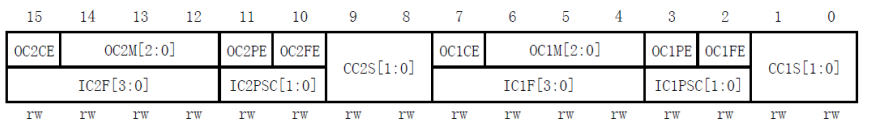
_Introduction to Capture/Compare Enabled Registers (TIMx_CCER), which controls the switching of input and output channels.
**TIMx CCER Register Description**
Capture/Compare Registers (TIMx_CCR1~4), which has four registers corresponding to four
Transport channels CH1~4.Because these four registers are all similar, just TIMx_CCR1 is introduced as an example.
**Register TIMx CCR1 Everyone Description**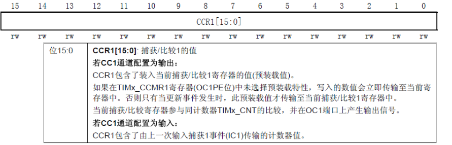
In output mode, the value of this register is compared with the value of CNT, and the corresponding actions are generated based on the comparison results.Using this, the output pulse width of the PWM can be controlled by modifying the value of this register.
_If you have a universal timer, configuring the above three registers is sufficient, but if you have an advanced timer, you also need to configure: Brake and Dead Zone Registers (TIMx_BDTR), the register is described in Figure 4.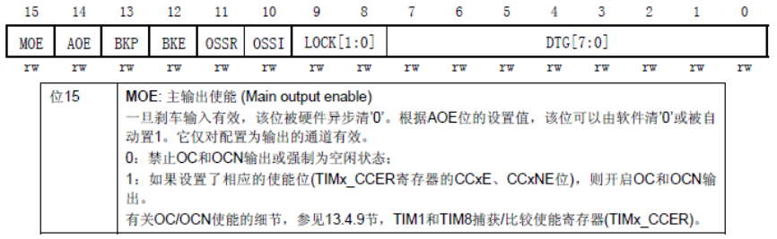
_This register, we only need to focus on the highest bit: MOE bit, in order for the PWM output of the advanced timer to be normal, the MOE bit must be set to 1, otherwise there will be no output.Note: This is not required for universal timers.
Configuration steps:
_1) Turn on TIM1 clock and configure PA8 for multiplexed output.To use TIM1, we must first turn on the TIM1 clock.Here we will also configure PA8 as a multiplexed output (and, of course, a PORTA clock) because of TIM1_The CH1 channel will use the multiplexing function of PA8 as output.The library functions enable TIM3 clocks by:
RCC_APB1PeriphClockCmd(RCC_APB1Periph_TIM3, ENABLE); //Enable timer 3 clock
Set PA8 as the multiplex function transport and list a line of code for GPIO initialization:
GPIO_InitStructure.GPIO_Mode = GPIO_Mode_AF_PP; //Multiplex push-pull output
_2) Set ARR and PSC for TIM1.
After turning on the TIM1 clock, we need to set the ARR and PSC registers to control the output PWM cycle.When the PWM cycle is too slow (less than 50Hz), we will clearly feel the flicker.Therefore, the PWM cycle should not be set too small here.This is done by TIM_in the library functionThe TimeBaseInit function is implemented.
TIM_TimeBaseStructure.TIM_Period = arr; //Set auto reload value
TIM_TimeBaseStructure.TIM_Prescaler =psc; //Set Pre-frequency Value
TIM_TimeBaseStructure.TIM_ClockDivision = 0; //Set clock division: TDTS = Tck_tim
TIM_TimeBaseStructure.TIM_CounterMode = TIM_CounterMode_Up; //Up Count Mode
TIM_TimeBaseInit(TIM1, &TIM_TimeBaseStructure); //Initializes TIMx's
_3) Set TIM1_The PWM mode and channel direction of CH1 enable CH1 output from TIM1.Next, we're going to set TIM1_CH1 is in PWM mode (frozen by default), configuring TIM1_Correlated bits of CCMR1 to control TIM1_Mode of CH1.In library functions, the PWM channel setting is through the function TIM_OC1Init()~TIM_OC4Init() to set, different channel settings function is different, here we use channel 1, so the function used is TIM_OC1Init().
void TIM_OC1Init(TIM_TypeDef* TIMx, TIM_OCInitTypeDef* TIM_OCInitStruct);
Look directly at the structure TIM_Definition of OCInitTypeDef:
t
ypedef struct
{
uint16_t TIM_OCMode;
uint16_t TIM_OutputState;
uint16_t TIM_OutputNState;
uint16_t TIM_Pulse;
uint16_t TIM_OCPolarity;
uint16_t TIM_OCNPolarity;
uint16_t TIM_OCIdleState;
uint16_t TIM_OCNIdleState;
} TIM_OCInitTypeDef;
Several member variables:
_Parameter TIM_OCMode setting mode is PWM or output comparison, here we are PWM mode.
_Parameter TIM_OutputState is used to set comparative output enabling, that is, enabling PWM output to the port.
_Parameter TIM_OCPolarity is used to set whether the polarity is high or low.
Other parameters TIM_OutputNState, TIM_OCNPolarity, TIM_OCIdleState and TIM_OCNIdleState is used by advanced timers TIM1 and TIM8.To achieve the scenarios we mentioned above, you can do this by:
T
IM_OCInitTypeDef TIM_OCInitStructure;
TIM_OCInitStructure.TIM_OCMode = TIM_OCMode_PWM2; //Select PWM mode 2
TIM_OCInitStructure.TIM_OutputState = TIM_OutputState_Enable; //Compare Output Enables
TIM_OCInitStructure.TIM_OCPolarity = TIM_OCPolarity_High; //High output polarity
TIM_OC1Init(TIM1, &TIM_OCInitStructure); //Initialize TIM1 OC1
_4) Enables TIM1.
After that, we need to enable TIM1.The method for enabling TIM1 has been explained earlier:
TIM_Cmd(TIM1, ENABLE); //Enable TIM1
_5) Set MOE output to enable PWM output.
After the normal timer is set above, you can output PWM, but for the advanced timer, we also need to enable the Brake and Dead Zone Registers (TIM1_The MOE bit of the BDTR to enable the entire OCx (or PWM) output.The number is set to:
TIM_CtrlPWMOutputs(TIM1,ENABLE);// MOE Primary Output Enabling
_6) Modify TIM1_CCR1 controls duty cycle.
_Finally, after the above settings, PWM has actually started to output, but its duty cycle and frequency are fixed, and we modify TIM1_CCR1 controls the output duty cycle of CH1.The PWM output is then controlled.
In the library function, modify TIM1_The function of CCR1 duty cycle is:
void TIM_SetCompare1(TIM_TypeDef* TIMx, uint16_t Compare1);
Of course, for other channels, there is a function name in the form TIM_SetComparex(x=1,2,3,4).With the above six steps, we can control the CH1 output PWM wave of TIM1.
main function
#include "led.h"
#include "delay.h"
#include "sys.h"
#include "pwm.h"

 int main(void)
 {
	u16 led0pwmval=0;
	u8 dir=1;
	delay_init();	    	 //Delay function initialization
	LED_Init();		  	//Initialize the hardware interface to connect to the LED
	TIM1_PWM_Init(899,0);//No frequency division.PWM Frequency=72000/(899+1)=80Khz
   	while(1)
	{
 		delay_ms(10);
		if(dir)led0pwmval++;
		else led0pwmval--;

 		if(led0pwmval>300)dir=0;
		if(led0pwmval==0)dir=1;
		TIM_SetCompare1(TIM1,led0pwmval);	  //Channel Compare Value Modify TIM1_CCR1 duty cycle
	}
}
pwm.c
#include "pwm.h"
#include "led.h"
//PWM Output Initialization
//arr: auto-reload value
//psc: clock Prescale frequency
void TIM1_PWM_Init(u16 arr,u16 psc)
{
	 GPIO_InitTypeDef GPIO_InitStructure;
	TIM_TimeBaseInitTypeDef  TIM_TimeBaseStructure;
	TIM_OCInitTypeDef  TIM_OCInitStructure;

	RCC_APB2PeriphClockCmd(RCC_APB2Periph_TIM1, ENABLE);// Enabling timer 1
 	RCC_APB2PeriphClockCmd(RCC_APB2Periph_GPIOA , ENABLE);  //Enabling GPIO peripheral clock enabling


   //Set the pin as the multiplex output function to output the PWM pulse waveform of TIM1 CH1
	GPIO_InitStructure.GPIO_Pin = GPIO_Pin_8; //TIM_CH1
	GPIO_InitStructure.GPIO_Mode = GPIO_Mode_AF_PP;  //Multiplex push-pull output
	GPIO_InitStructure.GPIO_Speed = GPIO_Speed_50MHz;
	GPIO_Init(GPIOA, &GPIO_InitStructure);


	TIM_TimeBaseStructure.TIM_Period = arr; //Set the value of the auto reload register cycle for the next update event load activity 80KHZ
	TIM_TimeBaseStructure.TIM_Prescaler =psc; //Set the Prescale value to be used as the TIMx clock frequency divisor
	TIM_TimeBaseStructure.TIM_ClockDivision = 0; //Set clock division: TDTS = Tck_tim
	TIM_TimeBaseStructure.TIM_CounterMode = TIM_CounterMode_Up;  //TIM Up Count Mode
	TIM_TimeBaseInit(TIM1, &TIM_TimeBaseStructure); //According to TIM_Unit of time base for initializing TIMx with parameters specified in TimeBaseInitStruct


	TIM_OCInitStructure.TIM_OCMode = TIM_OCMode_PWM2; //Select timer mode: TIM pulse width modulation mode 2
	TIM_OCInitStructure.TIM_OutputState = TIM_OutputState_Enable; //Compare Output Enables
	TIM_OCInitStructure.TIM_Pulse = 0; //Set the pulse value of the capture comparison register to load
	TIM_OCInitStructure.TIM_OCPolarity = TIM_OCPolarity_High; //Output Polarity: TIM output is more polar
	TIM_OC1Init(TIM1, &TIM_OCInitStructure);  //According to TIM_Parameters specified in OCInitStruct initialize peripheral TIMx channel 1

  TIM_CtrlPWMOutputs(TIM1,ENABLE);	//MOE Primary Output Enabling

	TIM_OC1PreloadConfig(TIM1, TIM_OCPreload_Enable);  //CH1 Preloading Enables

	TIM_ARRPreloadConfig(TIM1, ENABLE); //Preload register enabling TIMx on ARR

	TIM_Cmd(TIM1, ENABLE);  //Enable TIM1


}
pwm.h
#ifndef __PWM_H
#define __PWM_H
#include "sys.h"

void TIM1_PWM_Init(u16 arr,u16 psc);

#endif
Note: Code source, positive atom.