Experimental on-chip temperature sensor
The code was found online, and then I thought about it myself.
/***********System clock initialization*********************************/
void InitClock(void)
{
    CLKCONCMD &= ~0x40;              //Set the system clock source to 32MHZ crystal oscillator
    while(CLKCONSTA & 0x40);         //Wait for the crystal oscillator to stabilize
    CLKCONCMD &= ~0x47;              //Set the system master clock frequency to 32MHZ
}
/***************Timer initialization**********************/
void InitT3(void)
{
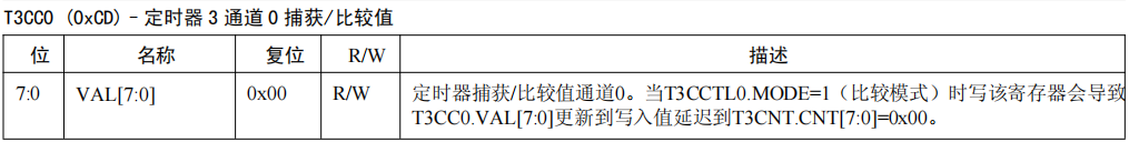
T3CCTL0 = 0x44; //0100 0100 T3CCTL0 (0xCC), CH0 interrupt enable, CH0 comparison mode
T3CC0 = 0xFA; //T3CC0 set to 250
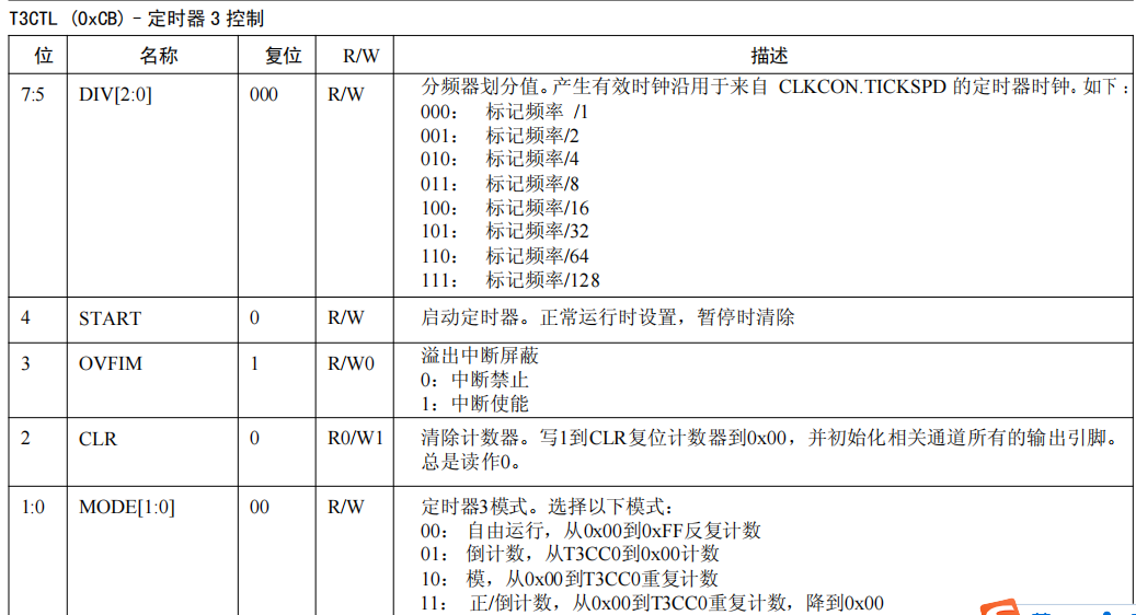
T3CTL |= 0x9A; //Start the T3 counter, and the counting clock is 16 frequency division. Using MODULO mode
IEN1 |= 0x08;
IEN0 |= 0x80; //Open total interrupt, open T3 interrupt
}

/****************Temperature sensor initialization function*******************/
void InitSensor(void)
{
DISABLE_ALL_INTERRUPTS(); //Turn off all interrupts
InitClock(); //Set the system master clock to 32M
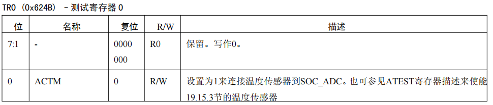
TR0=0x01; //Set to 1 to connect the temperature sensor to the SOC_ADC
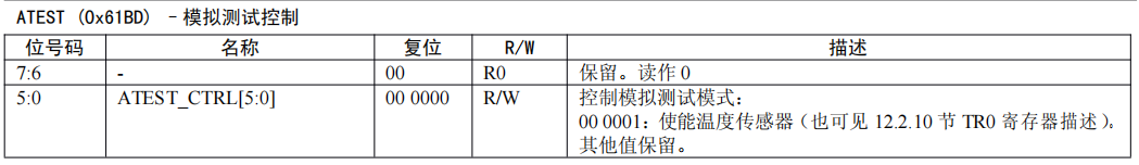
ATEST=0x01; //Enable temperature sensing
}
/**************Get the sensor temperature value and return***********************/
float GetTemperature(void)
{
uint value;
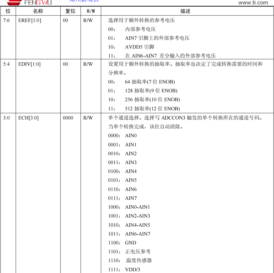
ADCCON3 = (0x3E); //0011 1110 select 1.25V as the reference voltage; 14 bit resolution; Sample the on-chip temperature sensor
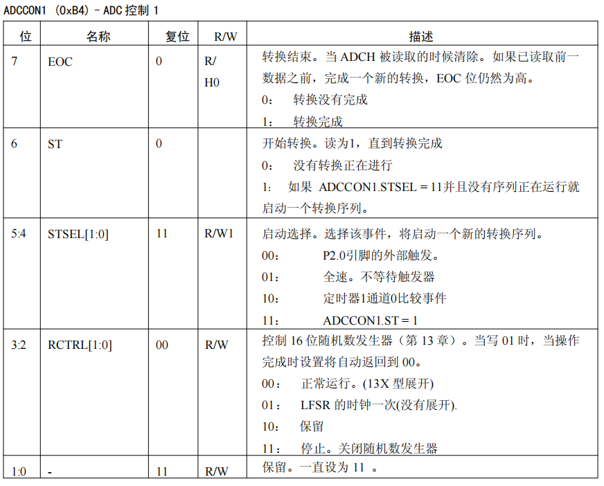
ADCCON1 |= 0x30; //0011 0000 select ADC startup mode as manual
ADCCON1 |= 0x40; //Start AD conversion
while(!(ADCCON1 & 0x80)); //Wait for AD conversion to complete
value = ADCL >> 4; //The lower 2 bits of ADCL register are invalid. Since only 12 bits are valid, the lower 4 bits of ADCL register are invalid.
value |= (((uint)ADCH) << 4);
return (value-1367.5)/4.5-5; //According to the AD value, calculate the actual temperature. There is an error in the chip manual. The temperature coefficient should be 4.5 / ℃
//For temperature correction, subtract 5 ℃ (different chips are corrected according to specific conditions)
}
ADCCON3
ADCCON1
Complete code
#include <ioCC2530.h>
#include <stdio.h>
#include <string.h>

typedef unsigned char uchar;
typedef unsigned int  uint;

#define DISABLE_ALL_INTERRUPTS() (IEN0 = IEN1 = IEN2 = 0x00) / / off interrupt

/*************************Delay*************************************/
void DelayMS(uint msec)
{
    uint i,j;

    for (i=0; i<msec; i++)
        for (j=0; j<1060; j++);
}

/***********System clock initialization*********************************/
void InitClock(void)
{
    CLKCONCMD &= ~0x40;              //Set the system clock source to 32MHZ crystal oscillator
    while(CLKCONSTA & 0x40);         //Wait for the crystal oscillator to stabilize
    CLKCONCMD &= ~0x47;              //Set the system master clock frequency to 32MHZ
}

/***************Timer initialization**********************/
void InitT3(void)
{
    T3CCTL0 = 0x44;        //T3CCTL0 (0xCC), CH0 interrupt enable, CH0 comparison mode
    T3CC0 = 0xFA;          //T3CC0 set to 250
    T3CTL |= 0x9A;         //Start the T3 counter, and the counting clock is 16 frequency division. Using MODULO mode
    IEN1 |= 0x08;
    IEN0 |= 0x80;          //Open total interrupt, open T3 interrupt
}

/***********Serial port initialization***********************************************/
void InitUART(void)
{
    PERCFG = 0x00;                   //Position 1 Port P0
    P0SEL = 0x3C;                    //P0 is used as serial port

    P2DIR &= ~0xC0;                  //P0 is preferred as UART0
    U0CSR |= 0x80;                   //The serial port is set to UART mode
    U0GCR |= 11;
    U0BAUD |= 216;                   //The baud rate is set to 115200

    UTX0IF = 0;                      //UART0 TX interrupt flag initial setting 0
    U0CSR |= 0x40;                   //Allow reception
    IEN0 |= 0x84;                    //Receive interrupt
}

/****************Temperature sensor initialization function*******************/
void InitSensor(void)
{
   DISABLE_ALL_INTERRUPTS();     //Turn off all interrupts
   InitClock();                  //Set the system master clock to 32M
   TR0=0x01;                     //Set to 1 to connect the temperature sensor to the SOC_ADC
   ATEST=0x01;                   //Enable temperature sensing
}


/****************Serial port sending function*******************************/
void UartSendString(char *Data, int len)
{
    uint i;

    for(i=0; i<len; i++)
    {
        U0DBUF = *Data++;
        while(UTX0IF == 0);
        UTX0IF = 0;
    }

    U0DBUF = 0x0A;                   //Output wrap
    while(UTX0IF == 0);
    UTX0IF = 0;
}


/**************Get the sensor temperature value and return***********************/
float GetTemperature(void)
{
   uint  value;

   ADCCON3  = (0x3E);            //Select 1.25V as the reference voltage; 14 bit resolution; Sample the on-chip temperature sensor
   ADCCON1 |= 0x30;              //Select ADC startup mode as manual
   ADCCON1 |= 0x40;              //Start AD conversion
   while(!(ADCCON1 & 0x80));     //Wait for AD conversion to complete
   value =  ADCL >> 4;           //The lower 2 bits of ADCL register are invalid. Since only 12 bits are valid, the lower 4 bits of ADCL register are invalid. Many codes on the network are shifted two bits to the right, which is wrong
   value |= (((uint)ADCH) << 4);

   return (value-1367.5)/4.5-5;  //According to the AD value, calculate the actual temperature. There is an error in the chip manual. The temperature coefficient should be 4.5 / ℃
                                 //For temperature correction, subtract 5 ℃ (different chips are corrected according to specific conditions)
}

/****************************************************************************
* Program entry function
****************************************************************************/
void main(void)
{
    char i;
    float fSum, AvgTemp;
    char strTemp[6];

    InitUART();                           //Initialize serial port
    InitSensor();                         //Initialize ADC

    while(1)
    {
        fSum = 0;
        for (i=0; i<64; i++)
        {
            fSum += GetTemperature();     //Take the sum of 64 times of temperature
        }
        AvgTemp = fSum/64;                //Take the average temperature of 64 times

        memset(strTemp, 0, 6);
        sprintf(strTemp,"%.02f", AvgTemp);//Converts a floating-point number to a string, retaining 2 decimal places
        UartSendString(strTemp, 5);       //Send it to the computer through the serial port to display the chip temperature
        DelayMS(1000);                    //delayed
    }
}
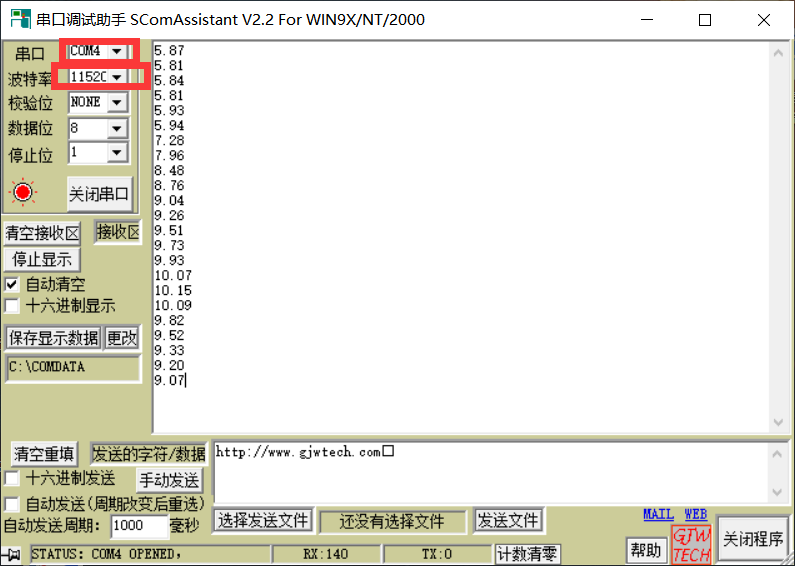
These two things should be based on your own serial port. My ZigBee USB cable is connected to COM4, and the baud rate code is 115200
ADC
cc2530 in the Chinese manual.
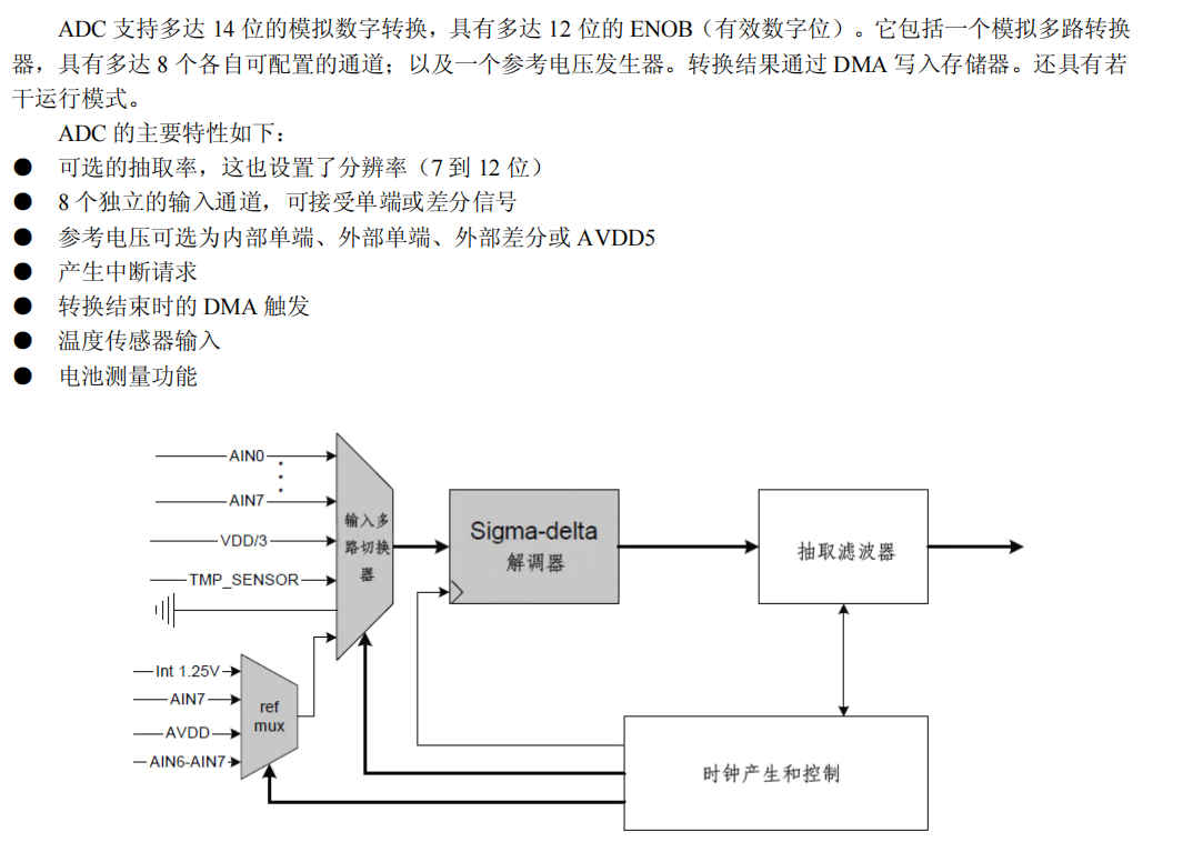
12.2 ADC operation
This section describes the general installation and operation of ADC, and describes the ADC control accessed by CPU and the use of status registers.
12.2.1 ADC input
The signal of port 0 pin can be used as ADC input. In the following description, these port pins refer to AIN0-AIN7 pins. Input pins AIN0-AIN7 are connected to the ADC.
The input can be configured as single ended or differential input. When the differential input is selected, the differential input includes input pairs AIN0-1, AIN2-3, AIN4-5 and AIN6-7.
Note that negative voltages do not apply to these pins, nor do voltages greater than VDD (unregulated voltage). The difference between them is the difference between input pairs converted in differential mode. It is the difference between input pairs converted in differential mode.
In addition to the input pins AIN0-AIN7, the output of the on-chip temperature sensor can also be selected as the input of the ADC for temperature measurement. This register tr0 Adctm and atest Atestctrl must be set separately as required.
A voltage corresponding to AVDD5/3 can also be input as an ADC input. This input allows functions such as the need to implement a battery monitor in the application. Note that in this case, the reference voltage cannot depend on the power supply voltage, for example, the AVDD5 voltage cannot be used as a reference voltage.
Single ended voltage inputs AIN0 to AIN7 are represented by channel numbers 0 to 7. Channel numbers 8 to 11 represent differential inputs and consist of AIN0 – AIN1, AIN2 – AIN3, AIN4 – AIN5 and AIN6 – AIN7. Channel numbers 12 to 15 represent G N D (12) temperature sensor (14), and AVDD5/3
(15) . these values are used in the ADCCON2.SCH and ADCCON3.SCH domains.
12.2.2 ADC conversion sequence
The ADC will perform a series of transformations and move the results to memory (via DMA) without any CPU intervention.
The conversion sequence can be affected by the APCFG register. The eight bit analog input comes from the I/O pin and does not have to be programmed into analog input. If a channel should normally be part of the sequence, but the corresponding analog input is disabled in APCFG, the channel will be skipped.
When using differential input, both pins in the differential pair must be set as analog input pins in the APCFG register.
ADCCON2. The SCH register bit is used to define an ADC conversion sequence from the ADC input.
If adccon2 Sch is set to a value less than 8, and the conversion sequence includes a conversion from each channel, from 0 to up, including adccon2 Sch programmed channel number.
When adccon2 Sch is set to a value between 8 and 12, and the sequence includes differential inputs, starting at channel 8 and ending at the programmed channel.
For adccon2 Sch is greater than or equal to 12, and the sequence includes only the selected channel
12.2. 3 single ADC conversion
In addition to this conversion sequence, the ADC can be programmed to perform a conversion from any channel. Such a conversion is done by writing the ADCCON3 register
Trigger. Unless a transformation sequence is already in progress, the transformation starts immediately, in which case a single transformation is executed as soon as the sequence is completed.
12.2.4 ADC operation mode
This section describes the operation mode and initialization transition.
ADC has three control registers: ADCCON1, ADCCON2 and ADCCON3. These registers are used to configure the ADC and report the results.
ADCCON1.EOC bit is a status bit, which is set to high level when a conversion ends; When the ADCH is read, it is cleared.
ADCCON1. The st bit is used to start a conversion sequence. When this bit is set to high, adccon1 When stsel is 11 and no conversion is currently running, a sequence is started. When the sequence conversion is completed, this bit is automatically cleared.
ADCCON1. The stsel bit selects which event will start a new conversion sequence. This option can be selected as external pin P2 0 rising edge or external pin event, end event of previous sequence, channel 0 comparison event of timer 1 or adccon1 ST is 1.
The ADCCON2 register controls how the conversion sequence is performed.
ADCCON2.SREF is used to select the reference voltage. The reference voltage can only be modified without conversion operation.
ADCCON2. The sdiv bit selects the decimation rate (and therefore also sets the resolution and the time required to complete a conversion, or the sample rate). The decimation rate can only be modified when there is no conversion operation. The last channel of the conversion sequence is selected by the ADCCON2.SCH bit, as described above.
The ADCCON3 register controls the channel number, reference voltage and extraction rate of a single conversion. A single conversion occurs immediately after the register ADCCON3 is written, or if a conversion sequence is in progress, immediately after the end of the sequence. The bit encoding of this register is exactly the same as that of ADCCON2.
12.2.5 ADC conversion results
The digital conversion result is expressed in the form of complement of 2. For single ended configurations, the result is always positive. This is because the result is the difference between the input signal and the ground, It is always a positive sign number (Vconv = vinp vinn, where Vinn=0V). The maximum value is reached when the input amplitude is equal to the selected voltage reference VREF. For differential configuration, the difference between two pin pairs is converted, and the difference can be a negative symbol number. For a 12 bit MSB of digital conversion result with extraction rate of 512, when analog input Vconv is equal to VREF, the digital conversion result is 2047. When When the analog input is equal to - VREF, the digital conversion result is - 2048. When adccon1 When EOC is set to 1, the digital conversion result is available, and the result is placed in ADCH and ADCL. Note that the conversion result always resides in the MSB segment of the combination of ADCH and ADCL registers. When reading adccon2 When the SCH bits are, they will indicate which channel the conversion is on. The results in ADCL and ADCH are generally applicable to
Previous conversion. If the conversion sequence has ended, adccon2 The value of SCH is greater than the last channel number, but if adccon2 is last written If the channel number of SCH is 12 or greater, the same value will be read back.
12.2.6 ADC reference voltage
The positive reference voltage of analog-to-digital conversion can be selected as an internally generated voltage, AVDD5 pin, external voltage applicable to AIN7 input pin, or differential voltage applicable to AIN6-AIN7 input pin. The accuracy of the conversion results depends on the stability of the reference voltage and the noise properties. The deviation of the desired voltage will lead to ADC gain error, which is directly proportional to the ratio of the desired voltage to the actual voltage. The noise of the reference voltage must be lower than the quantization noise of the ADC to ensure that the specified SNR is achieved.
12.2.7 ADC conversion time
ADC can only run on 32 MHz XOSC, and the user cannot divide the system clock. The 4 MHz frequency of the actual ADC sampling is generated by a fixed internal divider. The time required to perform a transformation depends on the selected extraction rate. In general, the conversion time is given by the following formula:
Tconv = (extraction rate + 16) x 0.25 μ s.
12.2.8 ADC interrupt
When a single conversion triggered by writing ADCCON3 is completed, the ADC will generate an interrupt. When a sequence conversion is completed, no interrupt is generated.
12.2.9 ADC DMA trigger
Each time a sequence conversion is completed, the ADC will generate a DMA trigger. When a single conversion is completed, no DMA trigger is generated. For adccon2 Each of the eight channels defined by the possible settings of the first 8 bits in Sch has a DMA trigger. When a new sample in the channel is ready for conversion, DMA trigger is active. DMA trigger is named ADC in table 8-1_ CHSD, where s is a single ended channel and d is a differential channel.
In addition, there is a DMA trigger ADC_ Char, when new data is ready in any channel of ADC conversion sequence, it is active.