Learning content
This paper introduces the related contents of AXI BRAM controller. For the situation of small amount of data, discontinuous address and irregular length, data interaction is carried out through BRAM.
development environment
Vivado 18.3 & SDK, PYNQ-Z2 development board.
AXI BRAM controller
brief introduction
The BRAM controller can be used to interconnect with the AXI and integrate with the system master to communicate with the local block RAM. The kernel supports single and burst transmission to block RAM, and is optimized for performance.
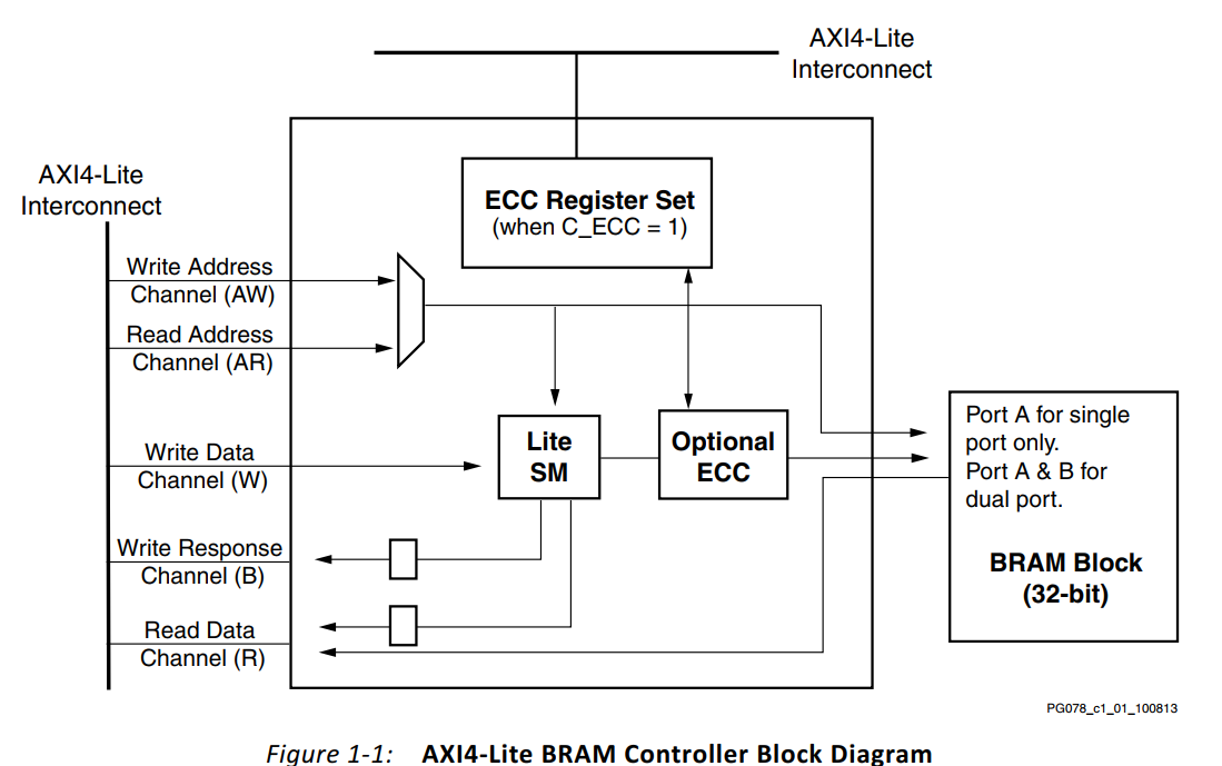
In an AX14 or AX14-Lite controller configuration, you can configure a single port to the BRAM block or two ports to the BRAM block. Through the second AX14 Lite control port connection, the AXI BRAM Controller IP can configure the ECC function on the data path and set it through the available external ECC registers. The top-level port connection and main module of the AXI BRAM Controller IP core are shown in the figure below. Shows the connection between the AXI BRAM core and the BRAM block in AX14 Lite mode. You can take advantage of the single port utilization of the BRAM block or the dual port mode of the BRAM block (through parameter settings).
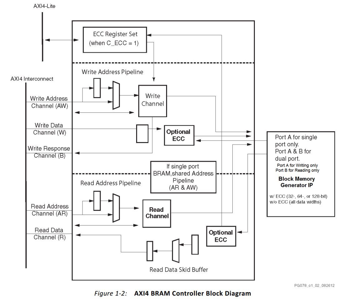
The following figure shows the HDL core generated to support the AX14 interface. For single port use of BRAM blocks, you can configure enhanced performance settings in dual port configuration., The detailed structure block diagram is as follows:
All communication with the axis master is through a 5-channel axis interface. All write operations are initiated on the write address channel (AW) of the AXI bus, which specifies the type of write transaction and the corresponding address information. The write data channel (W) communicates all write data for a single or burst write operation. The write response channel (B) is used as a handshake or response for write operations.
In the read operation, when the AXI main program requests read transmission, the read address channel (AR) communicates all address and control information. When a read operation can be processed, AXI responds to the read address channel (AR) from the AXI BRAM controller IP. Read data channel when read data is available ® The data and state of the transition operation.
Supported memory size
The maximum memory supported by AXI BRAM Controller is 2mbytes (byte size is 8 or 9). The supported memory width and depth are shown in Table 1-1.
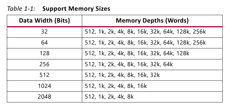
The minimum depth supported by the AXI BRAM Controller IP is 512 bytes. Any depth less than 512 is adjusted to 512 bytes.
Engineering block diagram
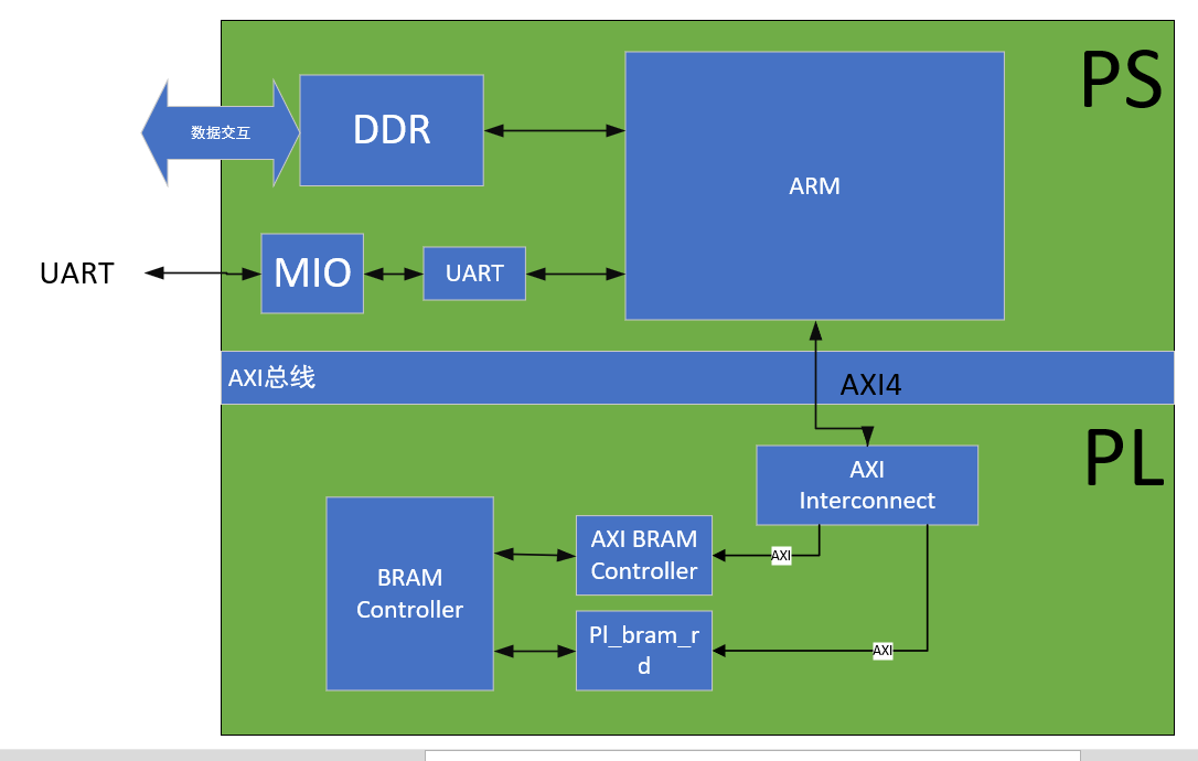
The engineering function design is that PS writes the data received by the serial port into BRAM, then reads the data from BRAM and prints it through the serial port; At the same time, PL also reads data from BRAM and observes whether the read data is consistent with the data printed by serial port through ILA.
The system block diagram is as follows:
Hardware platform construction
Create a new project and create a block design.
Configuring ZYNQ7
Add ZYNQ7 IP, initialize zynq, check configure uart resources,
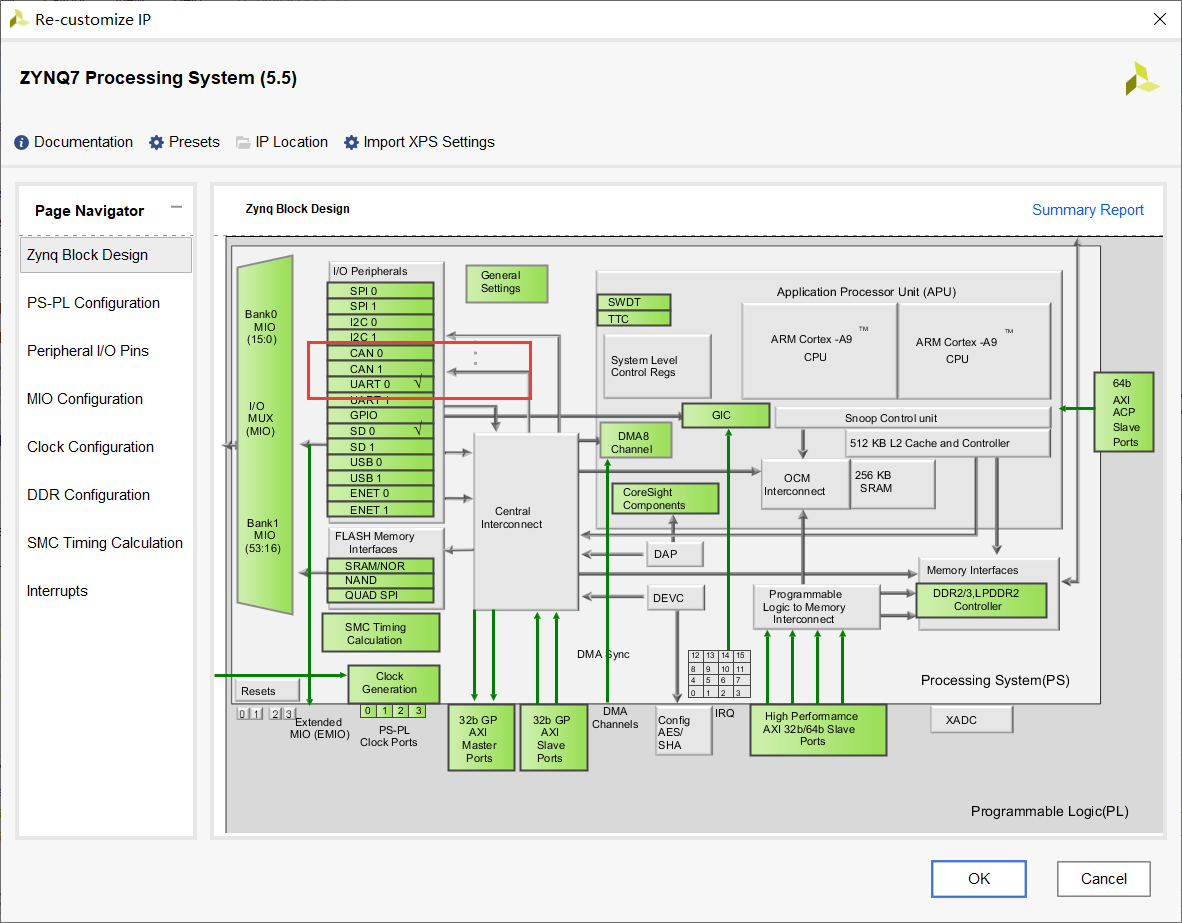
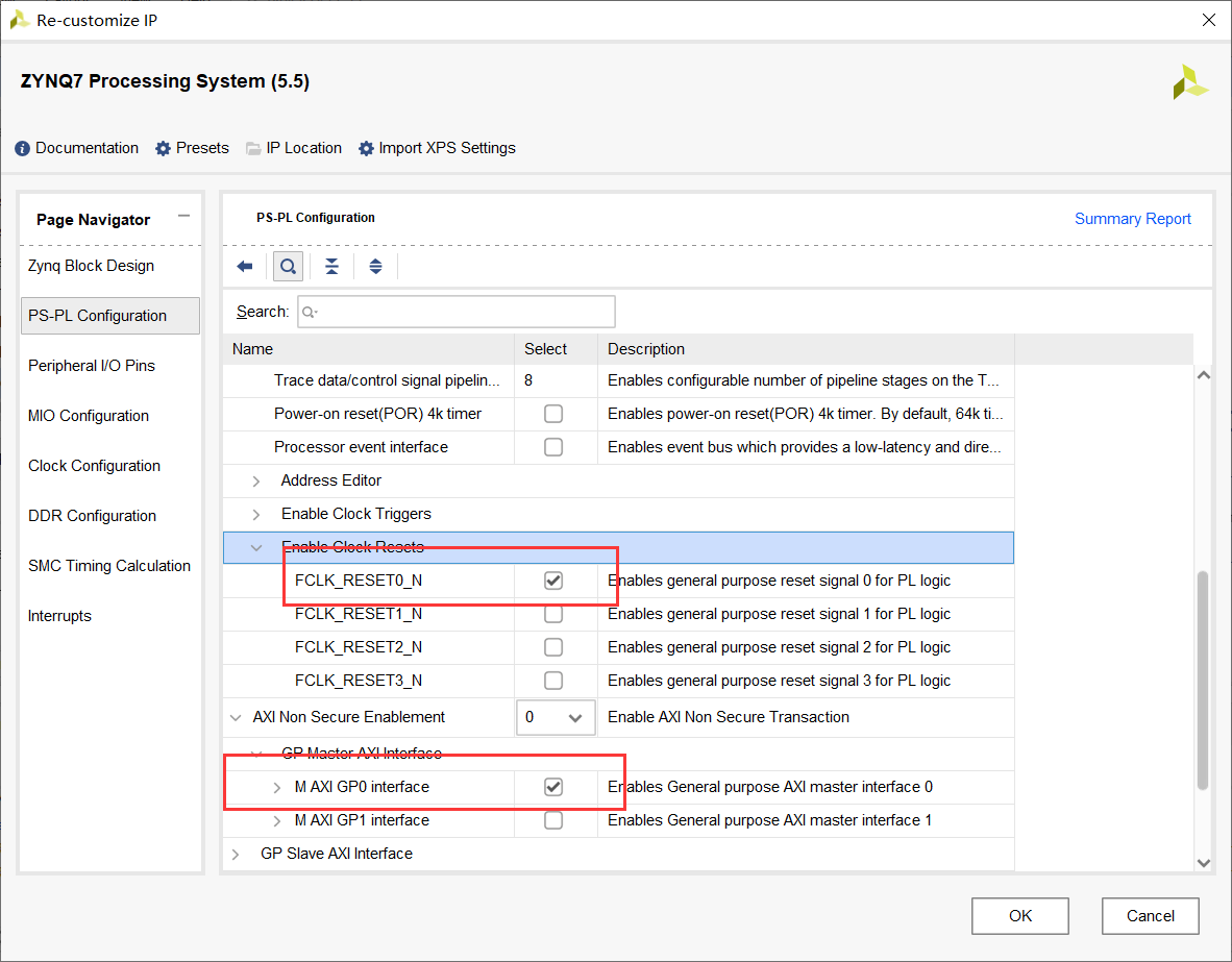
Enable clock reset and M_GP0 interface,
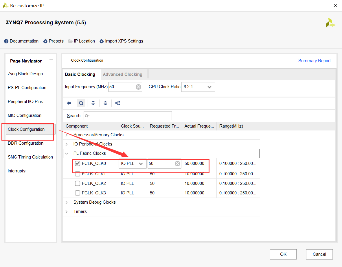
Configure the clock,
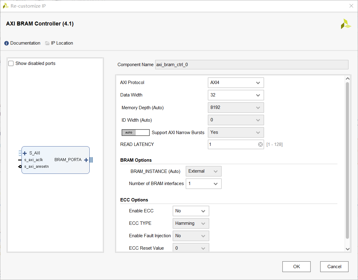
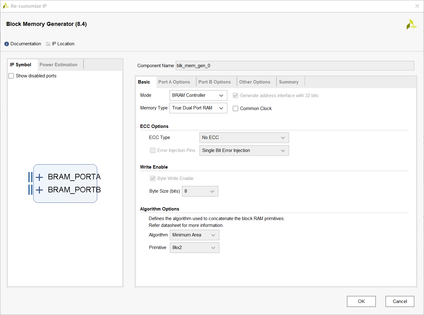
Configure BRAM controller and BRAM
Next, configure the BRAM controller, which is basically the default configuration.
Configure BRAM
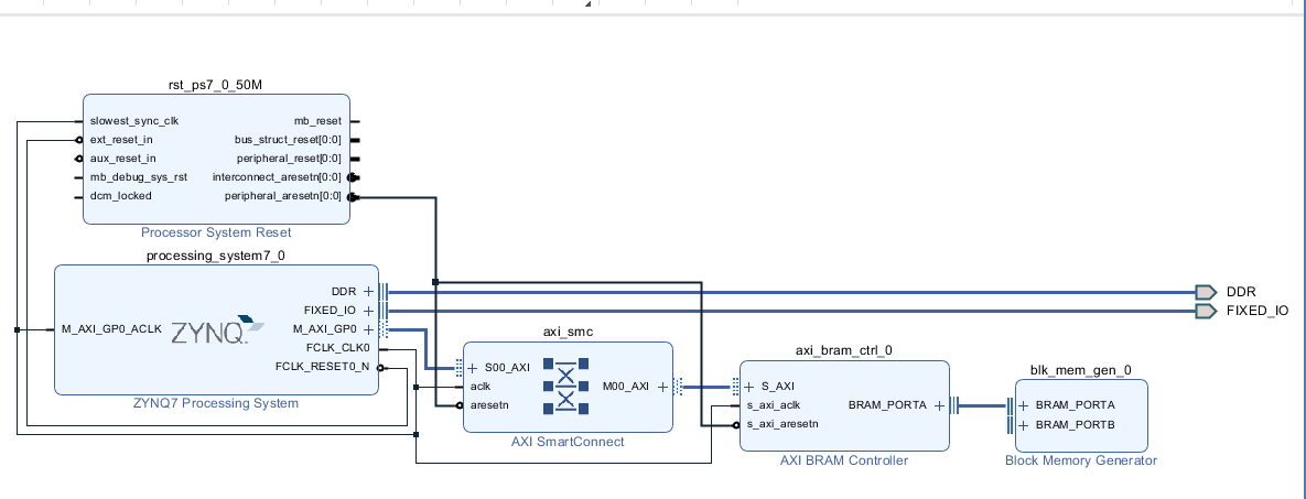
After connection, the system is as follows:,
Design reading control module
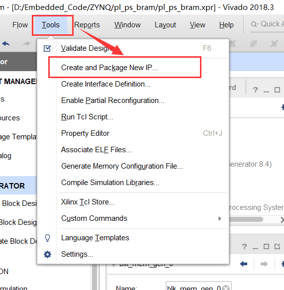
First, click tools to create a new IP,
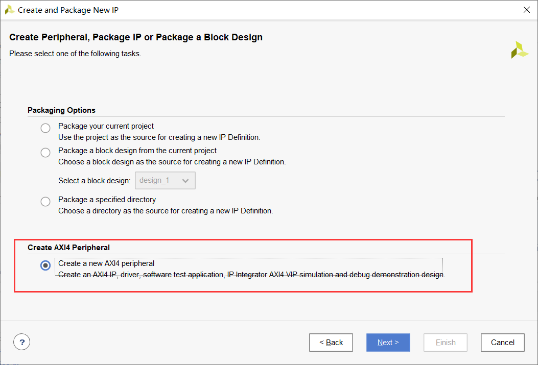
Select the IP address to create an AXI4 interface.
Edit IP name and other information, and design IP interface information,
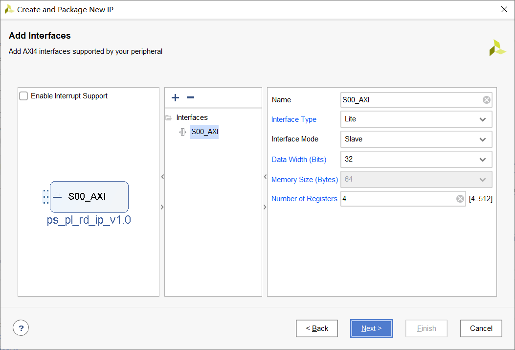
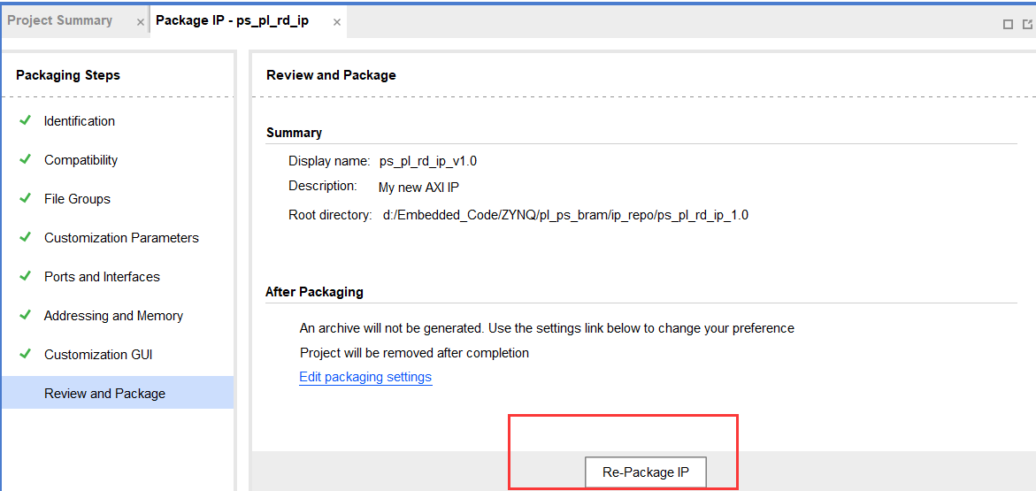
Click finish to complete the IP creation.
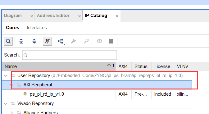
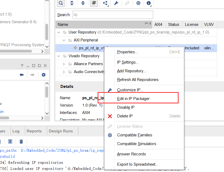
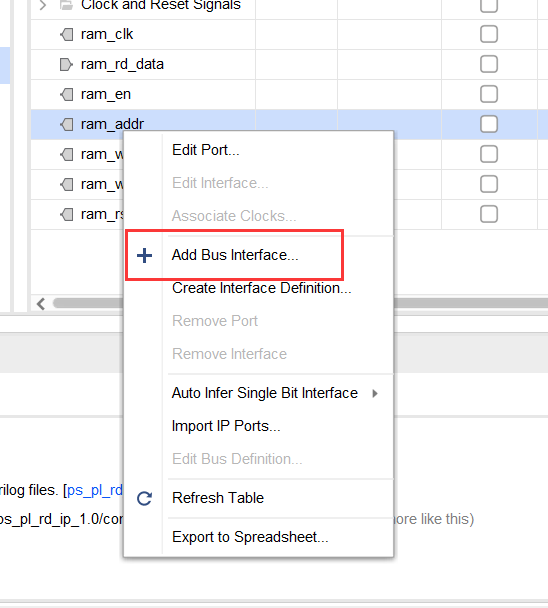
Find the created IP in the IP directory and right-click to edit the IP.
Instantiate the ram interface at the top level.
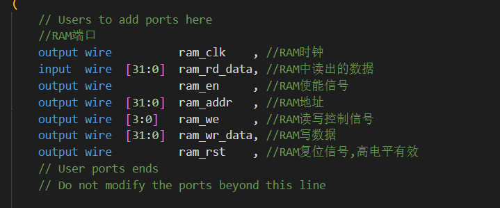
Add IP instantiation in the file of AXI bus protocol implementation to realize the function of AXI Lite interface and transfer parameters.
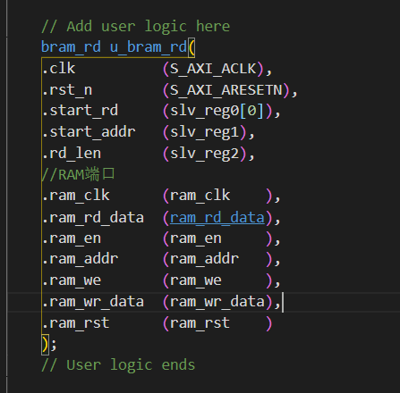
The reading module of BRAM of punctual atom is referenced here,
bram_rd.v
module bram_rd(
    input                clk        , //clock signal
    input                rst_n      , //Reset signal
    input                start_rd   , //Read start signal
    input        [31:0]  start_addr , //Read start address
    input        [31:0]  rd_len     , //Length of read data
    //RAM port
    output               ram_clk    , //RAM clock
    input        [31:0]  ram_rd_data, //Data read from RAM
    output  reg          ram_en     , //RAM enable signal
    output  reg  [31:0]  ram_addr   , //RAM address
    output  reg  [3:0]   ram_we     , //RAM read / write control signal
    output  reg  [31:0]  ram_wr_data, //RAM write data
    output               ram_rst      //RAM reset signal, high level active
);

//reg define
reg  [1:0]   flow_cnt;
reg          start_rd_d0;
reg          start_rd_d1;

//wire define
wire         pos_start_rd;

//*****************************************************
//**                  main code
//*****************************************************

assign  ram_rst = 1'b0;
assign  ram_clk = clk ;
assign pos_start_rd = ~start_rd_d1 & start_rd_d0;

//Delay two beats, start_ Rising edge of RD signal
always @(posedge clk or negedge rst_n) begin
    if(!rst_n) begin
        start_rd_d0 <= 1'b0;
        start_rd_d1 <= 1'b0;
    end
    else begin
        start_rd_d0 <= start_rd;
        start_rd_d1 <= start_rd_d0;
    end
end

//Read out data from RAM according to the read start signal
always @(posedge clk or negedge rst_n) begin
    if(!rst_n) begin
        flow_cnt <= 2'd0;
        ram_en <= 1'b0;
        ram_addr <= 32'd0;
        ram_we <= 4'd0;
    end
    else begin
        case(flow_cnt)
            2'd0 : begin
                if(pos_start_rd) begin
                    ram_en <= 1'b1;
                    ram_addr <= start_addr;
                    flow_cnt <= flow_cnt + 2'd1;
                end
            end
            2'd1 : begin
                if(ram_addr - start_addr == rd_len - 4) begin  //Data read out
                    ram_en <= 1'b0;
                    flow_cnt <= flow_cnt + 2'd1;
                end
                else
                    ram_addr <= ram_addr + 32'd4;              //Address accumulation 4
            end
            2'd2 : begin
                ram_addr <= 32'd0;
                flow_cnt <= 2'd0;
            end
        endcase
    end
end

endmodule
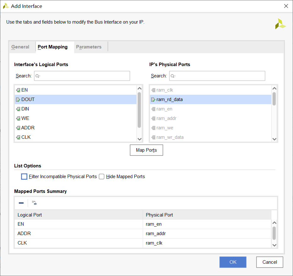
Create a pin interface, select any BRAM pin and create a package
Set the interface and name,
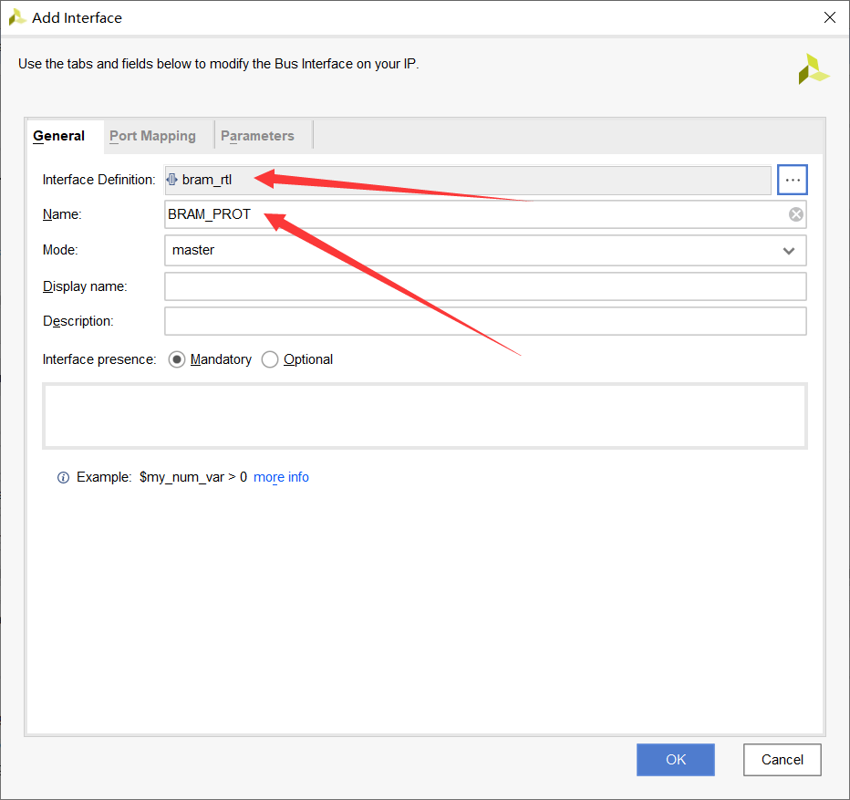
Complete interface mapping.
Then click Finish IP encapsulation.
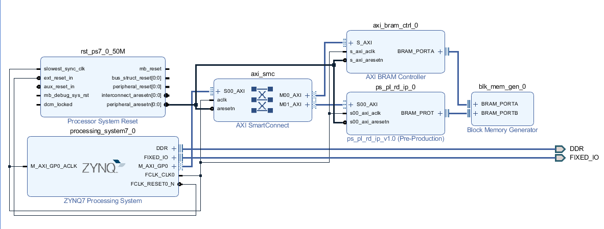
Complete system design
After creating the IP, add the IP and complete the connection. The overall design is shown in the figure below:
Then, after completing the synthesis, perform setup debug to grab the signals related to port b.
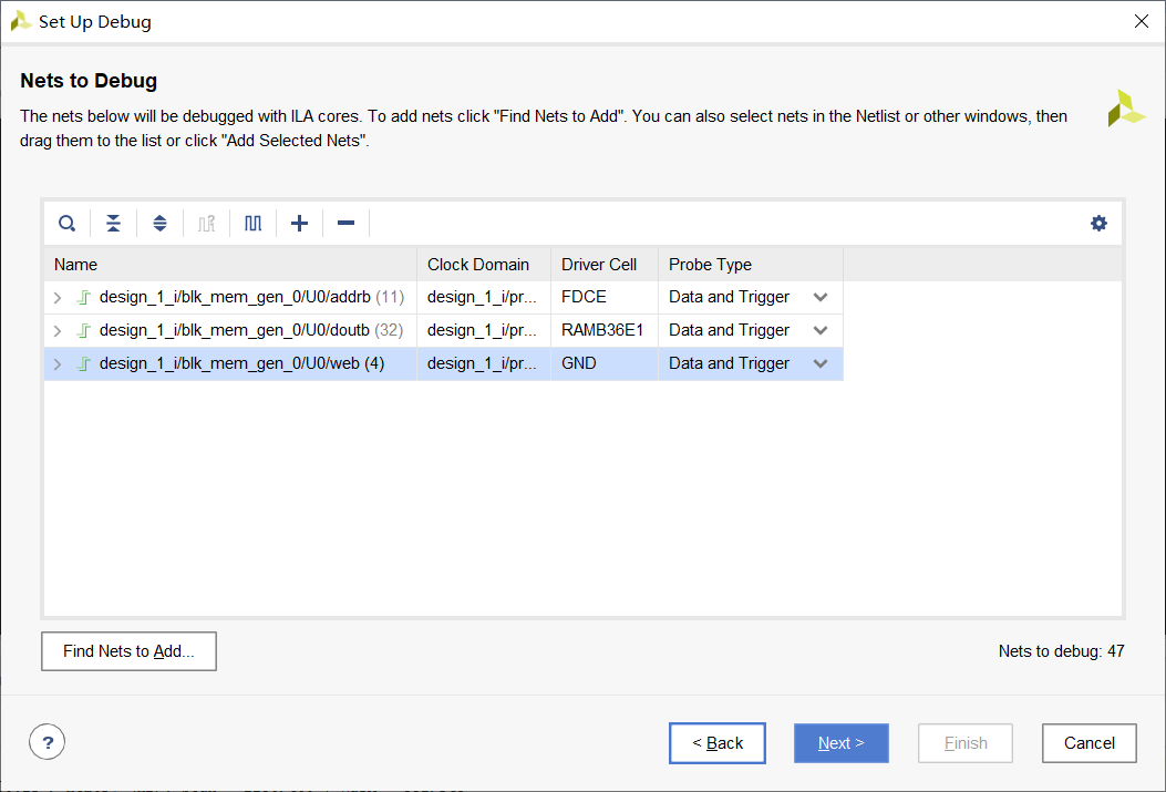
After adding the DEDUG signal, synthesize to generate the bit stream, then export the hardware and launch the SDK.
SDK software
New application project,
main.c enter the following code:
#include "xil_printf.h"
#include "stdio.h"
#include "xbram_hw.h"
#include "ps_pl_rd_ip.h"
#include "xparameters.h"

#define PL_BRAM_START  PS_PL_RD_IP_S00_AXI_SLV_REG0_OFFSET
#define PL_BRAM_START_ADDR PS_PL_RD_IP_S00_AXI_SLV_REG1_OFFSET
#define PL_BRAM_LEN PS_PL_RD_IP_S00_AXI_SLV_REG2_OFFSET
#define PS_PL_BASEADDR XPAR_PS_PL_RD_IP_0_S00_AXI_BASEADDR

#define START_ADDR  0
#define BRAM_DATA_BYTE 4
char input_data[1024];
int len_input_data;
int main(){
	while(1){
		int i=0;
		int wr_cnt=0;
		printf("ps_pl_bram test\n");
		scanf("%s",input_data);
		len_input_data= strlen(input_data);
		for(i = START_ADDR*BRAM_DATA_BYTE;i<(START_ADDR + len_input_data)*BRAM_DATA_BYTE;i+=BRAM_DATA_BYTE)
		{
			PS_PL_RD_IP_mWriteReg(XPAR_BRAM_0_BASEADDR,i,input_data[wr_cnt]);
			wr_cnt++;
		}
		//Configure start address
		PS_PL_RD_IP_mWriteReg(PS_PL_BASEADDR,PL_BRAM_START_ADDR,START_ADDR*BRAM_DATA_BYTE);
		//Configure read length
		PS_PL_RD_IP_mWriteReg(PS_PL_BASEADDR,PL_BRAM_LEN,len_input_data*BRAM_DATA_BYTE);
		//Enable pulse
		PS_PL_RD_IP_mWriteReg(PS_PL_BASEADDR,PL_BRAM_START,1);
		PS_PL_RD_IP_mWriteReg(PS_PL_BASEADDR,PL_BRAM_START,0);
		for(i = START_ADDR*BRAM_DATA_BYTE;i<(START_ADDR + len_input_data)*BRAM_DATA_BYTE;i+=BRAM_DATA_BYTE)
		{
			printf("bram address : %d ,read data : %c\n",i/BRAM_DATA_BYTE,PS_PL_RD_IP_mReadReg(XPAR_BRAM_0_BASEADDR,i));
		}
	}
}
Explanation of some codes
This project is relatively simple. The storage, display and printing of serial port input are realized in the while loop.
Operation effect
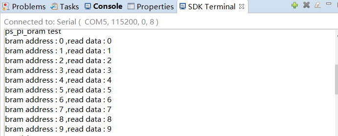
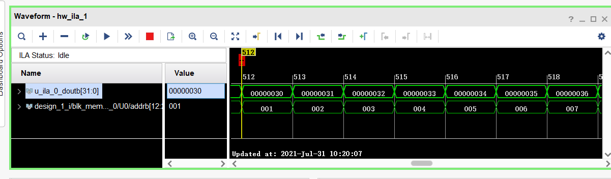
ila grabs data
The read data captured by ILA is consistent with the data sent and written.
references
- Punctual atomic development video
- Punctual atom embedded development guide
- UG585
- PG078