Written by @hzj
//JinXing Project
#2021.11.21 V1.0
1. Fixed point positioning of filter and use of Beyond compare
(1) Why fixed-point positioning?
1. Fixed point: the existence of fixed point is due to the binary operation inside FPGA. The decimal point (floating-point data) in the actual operation cannot be accurately represented by binary values. Therefore, according to the actual needs of the project, the reserved bit of floating-point number shall be set, and the data for saving floating-point data shall be set according to the quantization error. Of course, if you use more bits of binary numbers, the more accurate you can express a floating point number; On the contrary, if the number of bits of binary numbers is small, it can not accurately express a floating point number. Of course, this accuracy is based on a requirement. We can't ask for accuracy too much, but waste registers. Here is an example of a fixed point:
- > what is the minimum bit width required for lossless fixed-point conversion of floating-point number 12.918; If 11 bits are selected, what is the quantization error?
① Integer part: the integer of 12 needs to use 4 digits, that is, and 2 ^ 4 = 16 > 12. Therefore, the integer part needs to be represented by 4 decimal places.
② Decimal part: it is represented by 12 binary digits. Since the digit width of the integer part is 4 digits, the digit width of the decimal part is 8 digits. Therefore, the size of the value representing 0.918 decimal digits is int(0.918 * 256)/256 = 235/256 = 0.91796875. That is, if a 12 bit binary number is used to represent this value. If the binary number is really used, the size of the value is 0.91796875, which is 0.00003125 different from the actual value of 0.918. Due to the need for lossless fixed-point bits, the number of significant bits considered is three digits after the decimal point, and the size of the first three digits of the difference is 0, so it can be called lossless fixed-point------- At this time, what would it be like if we used 11 bit binary numbers for representation? If 11 bits are used, the integer bits of the former use 4 bits. Therefore, the decimal places here are represented by 7-bit binary numbers, and: int(0.918 * 128)/128 = 118/128 = 0.921875, which is 0.003875 different from the actual value of 0.918. It can be clearly seen here that the first three decimal places are not completely 0. Therefore, in this place, we conclude that 11 bit binary numbers cannot be lossless quantized, and the quantization error is 0.0039.
In fact, the number of floating-point numbers is represented by binary numbers. In essence, the size of floating-point numbers is represented by binary numbers. Therefore, floating-point numbers can be expanded in the same proportion, and the decimal places to be reserved can be expanded into integers. At the same time, when the decimal places to be reserved are expanded, the decimal places behind the decimal point can be intercepted, Then the original number is completely represented as an integer, which is equivalent to the realization of fixed-point operation. At the same time, it does not need to consider too much floating-point numbers, which is more convenient. In fact, the representation principle of the two is the same.
2. Positioning: the positioning here refers to the number of register bits during operation. For an operation, if the number of reserved register bits is too large, there will be a waste of devices, so it is necessary to "dig" bits. This place summarizes two operation principles:
① When m-bit binary numbers and n-bit binary numbers are added, the operation results need to use the register of max(m, n)+1-bit binary digits for data storage.
② When the m-bit binary number is multiplied by the n-bit binary number, the operation result needs to use the register of m+n-bit binary digits for data storage.
(2) Use of Beyond compare
The simulation designed in FPGA often needs one-to-one correspondence with the values in matlab to verify the correctness of FPGA simulation results. Therefore, it is necessary to simulate FPGA data operation in matlab, and then compare the simulated data in FPGA with FPGA simulation data one by one to judge whether it is correct. Beyond Compare is a data comparison software, which imports two txt files The data in the document will be displayed in red. You can clearly see which data is the same and which data is different.
2. Beyond Compare of 8bit parallel FIR filter and matlab simulation data
The 8-bit parallel input FIR filter has been implemented in the previous work. Therefore, it is necessary to carry out matlab simulation verification on the whole module to verify whether the filter functions. The verified data volume also selects the data of millions.
The relevant codes are as follows: 8-bit parallel FIR filter in FPGA:
main program
`timescale 1ns / 1ps
/*The parallel shift module successively inputs 8 signals to be filtered according to the clk signal, and 8 filtered signals come out in turn in each cycle. The module uses 8 convolution modules for operation, which is equivalent to the filtering content completed in the previous 8 cycles
 It can now be completed in one cycle.*/
module FIR_low8(
    input clk                            , //Input system clock, clock driven
    input rst_n                          , //The reset signal is defined to reset all parameters inside. The reset signal is valid at low level
    input signed [15:0] data_in_1        , //A clk signal, input the first data bit
    input signed [15:0] data_in_2        , //A clk signal, input the second data bit
    input signed [15:0] data_in_3        , //A clk signal, input the third data bit
    input signed [15:0] data_in_4        , //A clk signal, input the fourth data bit
    input signed [15:0] data_in_5        , //A clk signal, input the fifth data bit
    input signed [15:0] data_in_6        , //A clk signal, input the sixth data bit
    input signed [15:0] data_in_7        , //A clk signal, input the seventh data bit
    input signed [15:0] data_in_8        , //A clk signal, input the eighth data bit

    output reg signed [15:0] data_out_1    , //Define the filtered data, save it with reg variable, and the significant bit is 16bit
    output reg signed [15:0] data_out_2    , //Define the filtered data, save it with reg variable, and the significant bit is 16bit
    output reg signed [15:0] data_out_3    , //Define the filtered data, save it with reg variable, and the significant bit is 16bit
    output reg signed [15:0] data_out_4    , //Define the filtered data, save it with reg variable, and the significant bit is 16bit
    output reg signed [15:0] data_out_5    , //Define the filtered data, save it with reg variable, and the significant bit is 16bit
    output reg signed [15:0] data_out_6    , //Define the filtered data, save it with reg variable, and the significant bit is 16bit
    output reg signed [15:0] data_out_7    , //Define the filtered data, save it with reg variable, and the significant bit is 16bit
    output reg signed [15:0] data_out_8      //Define the filtered data, save it with reg variable, and the significant bit is 16bit
);

parameter U_DLY = 1;//Timing simulation signal, plus the delay of transmission in the circuit of U_DLY analog signal

/*16 data registers are defined to store the data of the signal to be filtered. For each clk cycle, 8 data to be filtered are input into the 8 registers x8, x7, x6...x1, that is to say
 The lower 8-bit register stores the latest data information, while the upper 8-bit register stores the data information of the previous clk cycle*/
reg signed [15:0] x1;
reg signed [15:0] x2;
reg signed [15:0] x3;
reg signed [15:0] x4;
reg signed [15:0] x5;
reg signed [15:0] x6;
reg signed [15:0] x7;
reg signed [15:0] x8;
reg signed [15:0] x9;
reg signed [15:0] x10;
reg signed [15:0] x11;
reg signed [15:0] x12;
reg signed [15:0] x13;
reg signed [15:0] x14;
reg signed [15:0] x15;
reg signed [15:0] x16;


/* Switch the data value in the register according to the clock signal. This shift uses the system clock and the falling edge rst_n resets and the LSB takes effect
 First, input the low eight bit data into the high eight bit register for storage (the register information of x1~x8 is put into the x9~x16 register), and input the 8-bit new data in this cycle
 Bits are input into the x8~x1 register in sequence.*/
always @ (posedge clk or negedge rst_n) begin
    if (rst_n == 1'b0) begin
        x1 <= #U_DLY 16'b0    ;
        x2 <= #U_DLY 16'b0    ;
        x3 <= #U_DLY 16'b0    ;
        x4 <= #U_DLY 16'b0    ;
        x5 <= #U_DLY 16'b0    ;
        x6 <= #U_DLY 16'b0    ;
        x7 <= #U_DLY 16'b0    ;
        x8 <= #U_DLY 16'b0    ;
        x9 <= #U_DLY 16'b0    ;
        x10 <= #U_DLY 16'b0   ;
        x11 <= #U_DLY 16'b0   ;
        x12 <= #U_DLY 16'b0   ;
        x13 <= #U_DLY 16'b0   ;
        x14 <= #U_DLY 16'b0   ;
        x15 <= #U_DLY 16'b0   ;
        x16 <= #U_DLY 16'b0   ;
    end
    else begin
        x9  <= #U_DLY x1                  ;
        x10 <= #U_DLY x2                  ;
        x11 <= #U_DLY x3                  ;
        x12 <= #U_DLY x4                  ;
        x13 <= #U_DLY x5                  ;
        x14 <= #U_DLY x6                  ;
        x15 <= #U_DLY x7                  ;
        x16 <= #U_DLY x8                  ;
        x1  <= #U_DLY data_in_8           ;
        x2  <= #U_DLY data_in_7           ;
        x3  <= #U_DLY data_in_6           ;
        x4  <= #U_DLY data_in_5           ;
        x5  <= #U_DLY data_in_4           ;
        x6  <= #U_DLY data_in_3           ;
        x7  <= #U_DLY data_in_2           ;
        x8  <= #U_DLY data_in_1           ;
    end
end


/* The adder adds the two according to the symmetry of quantization coefficients to obtain three variables add2_7, add3_6, add4_5. Since 8-bit parallel operation is required, 8 groups need to be prepared
 There are three adders for each set of registers, so a total of 3 * 8 = 24 registers are defined below */
wire signed [16:0] add2_7_1;
wire signed [16:0] add3_6_1;
wire signed [16:0] add4_5_1;
wire signed [16:0] add2_7_2;
wire signed [16:0] add3_6_2;
wire signed [16:0] add4_5_2;
wire signed [16:0] add2_7_3;
wire signed [16:0] add3_6_3;
wire signed [16:0] add4_5_3;
wire signed [16:0] add2_7_4;
wire signed [16:0] add3_6_4;
wire signed [16:0] add4_5_4;
wire signed [16:0] add2_7_5;
wire signed [16:0] add3_6_5;
wire signed [16:0] add4_5_5;
wire signed [16:0] add2_7_6;
wire signed [16:0] add3_6_6;
wire signed [16:0] add4_5_6;
wire signed [16:0] add2_7_7;
wire signed [16:0] add3_6_7;
wire signed [16:0] add4_5_7;
wire signed [16:0] add2_7_8;
wire signed [16:0] add3_6_8;
wire signed [16:0] add4_5_8;

/*Convolution output value register out_temp*/
wire signed [24:0] out_temp_1;
wire signed [24:0] out_temp_2;
wire signed [24:0] out_temp_3;
wire signed [24:0] out_temp_4;
wire signed [24:0] out_temp_5;
wire signed [24:0] out_temp_6;
wire signed [24:0] out_temp_7;
wire signed [24:0] out_temp_8;

/*The number to be added is stored in the register, the values in the register are switched in turn, and then input into the adder for addition operation*/
reg [15:0] num_x_2_1;
reg [15:0] num_x_3_1;
reg [15:0] num_x_4_1;
reg [15:0] num_x_5_1;
reg [15:0] num_x_6_1;
reg [15:0] num_x_7_1;

reg [15:0] num_x_2_2;
reg [15:0] num_x_3_2;
reg [15:0] num_x_4_2;
reg [15:0] num_x_5_2;
reg [15:0] num_x_6_2;
reg [15:0] num_x_7_2;

reg [15:0] num_x_2_3;
reg [15:0] num_x_3_3;
reg [15:0] num_x_4_3;
reg [15:0] num_x_5_3;
reg [15:0] num_x_6_3;
reg [15:0] num_x_7_3;

reg [15:0] num_x_2_4;
reg [15:0] num_x_3_4;
reg [15:0] num_x_4_4;
reg [15:0] num_x_5_4;
reg [15:0] num_x_6_4;
reg [15:0] num_x_7_4;

reg [15:0] num_x_2_5;
reg [15:0] num_x_3_5;
reg [15:0] num_x_4_5;
reg [15:0] num_x_5_5;
reg [15:0] num_x_6_5;
reg [15:0] num_x_7_5;

reg [15:0] num_x_2_6;
reg [15:0] num_x_3_6;
reg [15:0] num_x_4_6;
reg [15:0] num_x_5_6;
reg [15:0] num_x_6_6;
reg [15:0] num_x_7_6;

reg [15:0] num_x_2_7;
reg [15:0] num_x_3_7;
reg [15:0] num_x_4_7;
reg [15:0] num_x_5_7;
reg [15:0] num_x_6_7;
reg [15:0] num_x_7_7;

reg [15:0] num_x_2_8;
reg [15:0] num_x_3_8;
reg [15:0] num_x_4_8;
reg [15:0] num_x_5_8;
reg [15:0] num_x_6_8;
reg [15:0] num_x_7_8;

/*Start the work of 8bit convolution*/

/*Data of the first bit*/
assign add2_7_1 = {num_x_2_1[15] ,num_x_2_1} + {num_x_7_1[15], num_x_7_1};
assign add3_6_1 = {num_x_3_1[15], num_x_3_1} + {num_x_6_1[15], num_x_6_1};
assign add4_5_1 = {num_x_4_1[15], num_x_4_1} + {num_x_5_1[15], num_x_5_1};
//Instantiation call module, convolution layer_ one
mul mul_conv_1
(
    .add_2_7 (add2_7_1[16:0])   ,
    .add_3_6 (add3_6_1[16:0])   ,
    .add_4_5 (add4_5_1[16:0])   ,
    .mul_out (out_temp_1 [24:0])
);


/*Data of the second bit*/
assign add2_7_2 = {num_x_2_2[15] ,num_x_2_2} + {num_x_7_2[15], num_x_7_2};
assign add3_6_2 = {num_x_3_2[15], num_x_3_2} + {num_x_6_2[15], num_x_6_2};
assign add4_5_2 = {num_x_4_2[15], num_x_4_2} + {num_x_5_2[15], num_x_5_2};
//Instantiation call module, convolution layer_ two
mul mul_conv_2
(
    .add_2_7 (add2_7_2[16:0])   ,
    .add_3_6 (add3_6_2[16:0])   ,
    .add_4_5 (add4_5_2[16:0])   ,
    .mul_out (out_temp_2 [24:0])
);


/*Data of the third bit*/
assign add2_7_3 = {num_x_2_3[15] ,num_x_2_3} + {num_x_7_3[15], num_x_7_3};
assign add3_6_3 = {num_x_3_3[15], num_x_3_3} + {num_x_6_3[15], num_x_6_3};
assign add4_5_3 = {num_x_4_3[15], num_x_4_3} + {num_x_5_3[15], num_x_5_3};

//Instantiation call module, convolution layer_ three
mul mul_conv_3
(
    .add_2_7 (add2_7_3[16:0])   ,
    .add_3_6 (add3_6_3[16:0])   ,
    .add_4_5 (add4_5_3[16:0])   ,
    .mul_out (out_temp_3 [24:0])
);


/*Data of the fourth bit*/
assign add2_7_4 = {num_x_2_4[15] ,num_x_2_4} + {num_x_7_4[15], num_x_7_4};
assign add3_6_4 = {num_x_3_4[15], num_x_3_4} + {num_x_6_4[15], num_x_6_4};
assign add4_5_4 = {num_x_4_4[15], num_x_4_4} + {num_x_5_4[15], num_x_5_4};
//Instantiation call module, convolution layer_ four
mul mul_conv_4
(
    .add_2_7 (add2_7_4[16:0])   ,
    .add_3_6 (add3_6_4[16:0])   ,
    .add_4_5 (add4_5_4[16:0])   ,
    .mul_out (out_temp_4 [24:0])
);


/*Data of the fifth bit*/
assign add2_7_5 = {num_x_2_5[15] ,num_x_2_5} + {num_x_7_5[15], num_x_7_5};
assign add3_6_5 = {num_x_3_5[15], num_x_3_5} + {num_x_6_5[15], num_x_6_5};
assign add4_5_5 = {num_x_4_5[15], num_x_4_5} + {num_x_5_5[15], num_x_5_5};
//Instantiation call module, convolution layer_ five
mul mul_conv_5
(
    .add_2_7 (add2_7_5[16:0])   ,
    .add_3_6 (add3_6_5[16:0])   ,
    .add_4_5 (add4_5_5[16:0])   ,
    .mul_out (out_temp_5 [24:0])
);

/*Data of the sixth bit*/
assign add2_7_6 = {num_x_2_6[15] ,num_x_2_6} + {num_x_7_6[15], num_x_7_6};
assign add3_6_6 = {num_x_3_6[15], num_x_3_6} + {num_x_6_6[15], num_x_6_6};
assign add4_5_6 = {num_x_4_6[15], num_x_4_6} + {num_x_5_6[15], num_x_5_6};
//Instantiation call module, convolution layer_ six
mul mul_conv_6
(
    .add_2_7 (add2_7_6[16:0])   ,
    .add_3_6 (add3_6_6[16:0])   ,
    .add_4_5 (add4_5_6[16:0])   ,
    .mul_out (out_temp_6 [24:0])
);

/*Data of the seventh bit*/
assign add2_7_7 = {num_x_2_7[15] ,num_x_2_7} + {num_x_7_7[15], num_x_7_7};
assign add3_6_7 = {num_x_3_7[15], num_x_3_7} + {num_x_6_7[15], num_x_6_7};
assign add4_5_7 = {num_x_4_7[15], num_x_4_7} + {num_x_5_7[15], num_x_5_7};
//Instantiation call module, convolution layer_ seven
mul mul_conv_7
(
    .add_2_7 (add2_7_7[16:0])   ,
    .add_3_6 (add3_6_7[16:0])   ,
    .add_4_5 (add4_5_7[16:0])   ,
    .mul_out (out_temp_7 [24:0])
);

/*Data of the eighth bit*/
assign add2_7_8 = {num_x_2_8[15] ,num_x_2_8} + {num_x_7_8[15], num_x_7_8};
assign add3_6_8 = {num_x_3_8[15], num_x_3_8} + {num_x_6_8[15], num_x_6_8};
assign add4_5_8 = {num_x_4_8[15], num_x_4_8} + {num_x_5_8[15], num_x_5_8};
//Instantiation call module, convolution layer_ eight
mul mul_conv_8
(
    .add_2_7 (add2_7_8[16:0])   ,
    .add_3_6 (add3_6_8[16:0])   ,
    .add_4_5 (add4_5_8[16:0])   ,
    .mul_out (out_temp_8 [24:0])
);


/*According to the arrival of the clk signal, 8 groups of size bits and 6 bits are re input each time (originally 8 bits, but the values of the first and eighth bits of the quantization coefficient are 0, so they are omitted).
Following the serial input data, the first input is 9 ~ 16 (8 ~ 15), followed by 8 ~ 15 (7 ~ 14), 7 ~ 14 (6 ~ 13)... 3 ~ 8 (2 ~ 9)*/
always @ (posedge clk or negedge rst_n) begin
    if (rst_n == 1'b0) begin
        num_x_2_1 <= #U_DLY 0        ;
        num_x_3_1 <= #U_DLY 0        ;
        num_x_4_1 <= #U_DLY 0        ;
        num_x_5_1 <= #U_DLY 0        ;
        num_x_6_1 <= #U_DLY 0        ;
        num_x_7_1 <= #U_DLY 0        ;

        num_x_2_2 <= #U_DLY 0        ;
        num_x_3_2 <= #U_DLY 0        ;
        num_x_4_2 <= #U_DLY 0        ;
        num_x_5_2 <= #U_DLY 0        ;
        num_x_6_2 <= #U_DLY 0        ;
        num_x_7_2 <= #U_DLY 0        ;

        num_x_2_3 <= #U_DLY 0        ;
        num_x_3_3 <= #U_DLY 0        ;
        num_x_4_3 <= #U_DLY 0        ;
        num_x_5_3 <= #U_DLY 0        ;
        num_x_6_3 <= #U_DLY 0        ;
        num_x_7_3 <= #U_DLY 0        ;

        num_x_2_4 <= #U_DLY 0        ;
        num_x_3_4 <= #U_DLY 0        ;
        num_x_4_4 <= #U_DLY 0        ;
        num_x_5_4 <= #U_DLY 0        ;
        num_x_6_4 <= #U_DLY 0        ;
        num_x_7_4 <= #U_DLY 0        ;

        num_x_2_5 <= #U_DLY 0        ;
        num_x_3_5 <= #U_DLY 0        ;
        num_x_4_5 <= #U_DLY 0        ;
        num_x_5_5 <= #U_DLY 0        ;
        num_x_6_5 <= #U_DLY 0        ;
        num_x_7_5 <= #U_DLY 0        ;

        num_x_2_6 <= #U_DLY 0        ;
        num_x_3_6 <= #U_DLY 0        ;
        num_x_4_6 <= #U_DLY 0        ;
        num_x_5_6 <= #U_DLY 0        ;
        num_x_6_6 <= #U_DLY 0        ;
        num_x_7_6 <= #U_DLY 0        ;

        num_x_2_7 <= #U_DLY 0        ;
        num_x_3_7 <= #U_DLY 0        ;
        num_x_4_7 <= #U_DLY 0        ;
        num_x_5_7 <= #U_DLY 0        ;
        num_x_6_7 <= #U_DLY 0        ;
        num_x_7_7 <= #U_DLY 0        ;

        num_x_2_8 <= #U_DLY 0        ;
        num_x_3_8 <= #U_DLY 0        ;
        num_x_4_8 <= #U_DLY 0        ;
        num_x_5_8 <= #U_DLY 0        ;
        num_x_6_8 <= #U_DLY 0        ;
        num_x_7_8 <= #U_DLY 0        ;
    end
    else begin
        num_x_2_1 <= #U_DLY x10      ;
        num_x_3_1 <= #U_DLY x11      ;
        num_x_4_1 <= #U_DLY x12      ;
        num_x_5_1 <= #U_DLY x13      ;
        num_x_6_1 <= #U_DLY x14      ;
        num_x_7_1 <= #U_DLY x15      ;

        num_x_2_2 <= #U_DLY x9       ;
        num_x_3_2 <= #U_DLY x10      ;
        num_x_4_2 <= #U_DLY x11      ;
        num_x_5_2 <= #U_DLY x12      ;
        num_x_6_2 <= #U_DLY x13      ;
        num_x_7_2 <= #U_DLY x14      ;

        num_x_2_3 <= #U_DLY x8       ;
        num_x_3_3 <= #U_DLY x9       ;
        num_x_4_3 <= #U_DLY x10      ;
        num_x_5_3 <= #U_DLY x11      ;
        num_x_6_3 <= #U_DLY x12      ;
        num_x_7_3 <= #U_DLY x13      ;

        num_x_2_4 <= #U_DLY x7       ;
        num_x_3_4 <= #U_DLY x8       ;
        num_x_4_4 <= #U_DLY x9       ;
        num_x_5_4 <= #U_DLY x10      ;
        num_x_6_4 <= #U_DLY x11      ;
        num_x_7_4 <= #U_DLY x12      ;

        num_x_2_5 <= #U_DLY x6       ;
        num_x_3_5 <= #U_DLY x7       ;
        num_x_4_5 <= #U_DLY x8       ;
        num_x_5_5 <= #U_DLY x9       ;
        num_x_6_5 <= #U_DLY x10      ;
        num_x_7_5 <= #U_DLY x11      ;

        num_x_2_6 <= #U_DLY x5       ;
        num_x_3_6 <= #U_DLY x6       ;
        num_x_4_6 <= #U_DLY x7       ;
        num_x_5_6 <= #U_DLY x8       ;
        num_x_6_6 <= #U_DLY x9       ;
        num_x_7_6 <= #U_DLY x10      ;

        num_x_2_7 <= #U_DLY x4       ;
        num_x_3_7 <= #U_DLY x5       ;
        num_x_4_7 <= #U_DLY x6       ;
        num_x_5_7 <= #U_DLY x7       ;
        num_x_6_7 <= #U_DLY x8       ;
        num_x_7_7 <= #U_DLY x9       ;

        num_x_2_8 <= #U_DLY x3       ;
        num_x_3_8 <= #U_DLY x4       ;
        num_x_4_8 <= #U_DLY x5       ;
        num_x_5_8 <= #U_DLY x6       ;
        num_x_6_8 <= #U_DLY x7       ;
        num_x_7_8 <= #U_DLY x8       ;
    end
end

/*According to each clk rising edge signal, the convolution filtered data output is carried out. The output data needs to be shifted. The lower 9 bits of the 8-bit signal should be intercepted to achieve the purpose of reducing at the same time*/
always @ (posedge clk or negedge rst_n) begin
    if(rst_n == 1'b0) begin
        data_out_1 <= #U_DLY 0                     ;
        data_out_2 <= #U_DLY 0                     ;
        data_out_3 <= #U_DLY 0                     ;
        data_out_4 <= #U_DLY 0                     ;
        data_out_5 <= #U_DLY 0                     ;
        data_out_6 <= #U_DLY 0                     ;
        data_out_7 <= #U_DLY 0                     ;
        data_out_8 <= #U_DLY 0                     ;
    end
    else begin
        data_out_1 <= #U_DLY out_temp_1[24:9]       ;
        data_out_2 <= #U_DLY out_temp_2[24:9]       ;
        data_out_3 <= #U_DLY out_temp_3[24:9]       ;
        data_out_4 <= #U_DLY out_temp_4[24:9]       ;
        data_out_5 <= #U_DLY out_temp_5[24:9]       ;
        data_out_6 <= #U_DLY out_temp_6[24:9]       ;
        data_out_7 <= #U_DLY out_temp_7[24:9]       ;
        data_out_8 <= #U_DLY out_temp_8[24:9]       ;
    end
end
endmodule
Convolution instantiation module program
module  mul(
    input [16:0] add_2_7       ,
    input [16:0] add_3_6       ,
    input [16:0] add_4_5       ,

    output signed [24:0] mul_out
);

wire [23:0] mul_2_d;//Value after absolute value product
wire [23:0] mul_2;//The result of taking complement after product
wire [23:0] mul_3;
wire [23:0] mul_4;

/*Add three multiplications to complete the whole convolution operation. For mul_1. Since the quantization coefficient is 0, this place is omitted*/
assign mul_2_d = {{6{add_2_7[16]}}, add_2_7, 1'b0}            ;//11111110, where absolute values are multiplied first and then inversed
assign mul_2   = (~mul_2_d) + 1'b1                            ;//Reverse plus one

assign mul_3   = {{{7{add_3_6[16]}}, add_3_6}
                    + {{6{add_3_6[16]}}, add_3_6, 1'b0}
                    + {{3{add_3_6[16]}}, add_3_6, 4'b0}}       ;//1 0011

assign mul_4   = {{{3{add_4_5[16]}}, add_4_5, 4'b0}
                    + {{2{add_4_5[16]}}, add_4_5, 5'b0}
                    + {{1{add_4_5[16]}}, add_4_5, 6'b0}}        ;//111 0000

/*Add the above three multiplications to complete the whole convolution operation*/
assign mul_out = {mul_2[23], mul_2}
                 + {mul_3[23], mul_3}
                 + {mul_4[23], mul_4}                         ;

endmodule
Test tb file program
`timescale  1ns / 1ps

module tb_FIR_low8;

// FIR_low8 Parameters
parameter PERIOD  = 10;


// FIR_low8 Inputs
reg   clk                   ;
reg   clk_sig               ;
reg   rst_n                 ;
reg   signed [15:0]  data_in_1       ;
reg   signed [15:0]  data_in_2       ;
reg   signed [15:0]  data_in_3       ;
reg   signed [15:0]  data_in_4       ;
reg   signed [15:0]  data_in_5       ;
reg   signed [15:0]  data_in_6       ;
reg   signed [15:0]  data_in_7       ;
reg   signed [15:0]  data_in_8       ;
// FIR_low8 Outputs
wire  signed [15:0]  data_out_1      ;
wire  signed [15:0]  data_out_2      ;
wire  signed [15:0]  data_out_3      ;
wire  signed [15:0]  data_out_4      ;

wire  signed [15:0]  data_out_5      ;
wire  signed [15:0]  data_out_6      ;
wire  signed [15:0]  data_out_7      ;
wire  signed [15:0]  data_out_8      ;


integer i;
reg flag;

initial
begin
    clk                          = 0 ;
    clk_sig                      = 0 ;
    rst_n                        = 0 ;
    data_in_1                    = 0 ;
    data_in_2                    = 0 ;
    data_in_3                    = 0 ;
    data_in_4                    = 0 ;
    data_in_5                    = 0 ;
    data_in_6                    = 0 ;
    data_in_7                    = 0 ;
    data_in_8                    = 0 ;
    i                            = 1 ; //Here is counting from 1, that is, data_ The subscript of the first number in men is [1], not [0]
end

initial
begin
    forever #(PERIOD/2)  clk =~clk; // Period of CLK
end


initial
begin
    #(PERIOD*2) rst_n  =  1;  // Reset signal
end

initial
begin
    flag = 2'b0;
    #(PERIOD*4) flag <= 1'b1; //
end

parameter data_num = 32'd1000000;
reg [15:0] data_men[data_num:1];


initial begin
    $readmemb("C:/Users/64441/Desktop/8bit_beyondcompare/8bit/tb/sin.txt",data_men);   //Pay attention to the direction of the slash, not backward<<<<<<<
end

always@(posedge clk)begin
    if(flag == 1'b1)
    begin //Every CLK_ After the arrival of SIG signal, conduct a data input and input a new waveform data into data_in.
        data_in_1 <= data_men[i];
        data_in_2 <= data_men[i+1];
        data_in_3 <= data_men[i+2];
        data_in_4 <= data_men[i+3];
        data_in_5 <= data_men[i+4];
        data_in_6 <= data_men[i+5];
        data_in_7 <= data_men[i+6];
        data_in_8 <= data_men[i+7];
        i <= i+8;
    end
end

FIR_low8  u_FIR_low8 (
    .clk                     ( clk              ),
    .rst_n                   ( rst_n            ),
    .data_in_1               ( data_in_1   [15:0] ),
    .data_in_2               ( data_in_2   [15:0] ),
    .data_in_3               ( data_in_3   [15:0] ),
    .data_in_4               ( data_in_4   [15:0] ),
    .data_in_5               ( data_in_5   [15:0] ),
    .data_in_6               ( data_in_6   [15:0] ),
    .data_in_7               ( data_in_7   [15:0] ),
    .data_in_8               ( data_in_8   [15:0] ),

    .data_out_1                ( data_out_1  [15:0] ),
    .data_out_2                ( data_out_2  [15:0] ),
    .data_out_3                ( data_out_3  [15:0] ),
    .data_out_4                ( data_out_4  [15:0] ),
    .data_out_5                ( data_out_5  [15:0] ),
    .data_out_6                ( data_out_6  [15:0] ),
    .data_out_7                ( data_out_7  [15:0] ),
    .data_out_8                ( data_out_8  [15:0] )
);

integer w_file;
initial w_file = $fopen("C:/Users/64441/Desktop/8bit_beyondcompare/8bit/tb/simulation_out_8bit.txt");
always @(i)
begin
    $fdisplay(w_file,"%b",data_out_1);
    $fdisplay(w_file,"%b",data_out_2);
    $fdisplay(w_file,"%b",data_out_3);
    $fdisplay(w_file,"%b",data_out_4);
    $fdisplay(w_file,"%b",data_out_5);
    $fdisplay(w_file,"%b",data_out_6);
    $fdisplay(w_file,"%b",data_out_7);
    $fdisplay(w_file,"%b",data_out_8);
    if(i > 32'd1000000)    //Data written in total
        $stop;
end
endmodule
Here, we need to explain the program. Because the convolution operation is designed, it includes multiplication and addition. Therefore, we need to accurately calculate the bit width of each variable. First, for the input data, there are eight 16 bit wide data. Through symmetry analysis, symmetric addition is required. The register bit width after addition should be 17 bits to save the added value. When the added value is input into the convolution block mul.v for convolution operation, the size of the bit width needs to be analyzed, because the quantization coefficients are 0, - 2 and 19112 respectively. Through the binary processing of the four bit quantization coefficient, the maximum number of bit widths is 112 and the binary representation is 1110000. Therefore, the highest bit of shift multiplication in this place should be moved by 6 bits. Because it is an addition operation, one more sign bit is required in this place to avoid overflow of the value of the addition operation. Because the input bit width of the convolution block is 17 bits, the bit width after the product should be 17 + 6 + 1 = 24, so the output bit of the multiplication operation should be [23:0], and the result of the convolution operation is composed of the addition of multiple multiplication operations, that is, mul_out = {mul_2[23], mul_2} + {mul_3[23], mul_3} + {mul_4[23], mul_4}, so the output bits of the final convolution module should be [24:0], that is, 25 bits. Finally, use [24:9] to intercept the last 9 bits, which is equivalent to an overall division and scaling.
Matlab test simulation file
%Convert binary to decimal data
%%%%%%%%%%%%%%%%%%%%%%%%%%%%%%%%%%%%%%%%%%%%%%%%%%%%%%%%%%%%%%%%%%%%%%%%%%%%%%%%%%%%%%%%%%%%
str_in = importdata('..\tb\sin.txt');
str_length = length(str_in);
str_out = zeros(str_length, 1);
MAX_DATA = 2^15-1;
for number = 1 : str_length
    str_out(number) = bin2dec( num2str(str_in(number)) );
    if(str_out(number) > MAX_DATA)
           str_out(number) = bin2dec( num2str(str_in(number)) ) - 2^16;
    end
end
%%%%%%%%%%%%%%%%%%%%%%%%%%%%%%%%%%%%%%%%%%%%%%%%%%%%%%%%%%%%%%%%%%%%%%%%%%%%%%%%%%%%%%%%%%%%

x_in= str_out;

%Define an output signal y,Represents the place where the convoluted data is stored
y=zeros(1,str_length);

%Define an initial value
x_in_2 = 0;
x_in_3 = 0;
x_in_4 = 0;
x_in_5 = 0;
x_in_6 = 0;
x_in_7 = 0;
x_in_8 = 0;

for i=1:1:str_length

    %Convolution operation, convolute the data in the original register, and put the convoluted data into y(i)Yes.
     y(i) = x_in(i)*0 + x_in_2 * (-2) + x_in_3 * 19 +  x_in_4 * 112 + x_in_5 * 112 + x_in_6 * 19 + x_in_7 * (-2) + x_in_8 * 0;

     %Move the data in turn
     x_in_8 = x_in_7;
     x_in_7 = x_in_6;
     x_in_6 = x_in_5;
     x_in_5 = x_in_4;
     x_in_4 = x_in_3;
     x_in_3 = x_in_2;
     x_in_2 = x_in(i);
end

output=zeros(1,str_length);
for i = 1:1:str_length
	output(i) = y(i);
end

%The data after the convolution operation is binarized, converted into binary, and written to txt In the file
%Because in FPGA In, we have carried out the interception operation. Therefore, this place also needs to be intercepted
%The method of bit truncation adopted here is to control the writing, and achieve the purpose of bit truncation by controlling the number of data bits written,
%For example, the original output of this place output The maximum data stored in it should be represented by a 25 bit binary number
%However, the first 16 bits of data are intercepted, so the purpose of intercepting is achieved
fid = fopen('..\tb\simulation_bin_matlab.txt','w');
 for k=1:length(output)
    B_s=dec2bin(output(k)+((output(k))<0)*2^25,25);
    for j=1:16
       if B_s(j)=='1'
           tb=1;
       else
           tb=0;
       end
       fprintf(fid,'%d',tb);
    end
    fprintf(fid,'\r\n');
end
fprintf(fid,';');
fclose(fid);
It should be noted that since the output value is a 25 bit wide data, it also needs to do the cut-off division in the FPGA. Therefore, to realize the cut-off work, only the data written in the first 16 bits is saved directly when saving the data file, which is equivalent to cutting off the data of the last 9 bits.
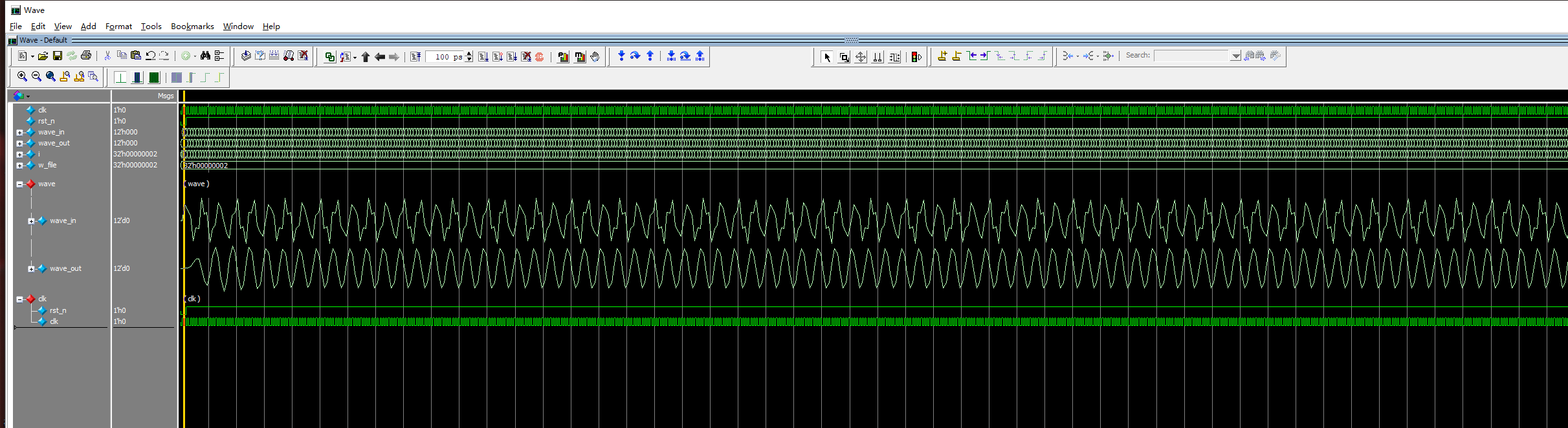
Verilog's test tb file saves the data into the txt document, and matlab also saves the data into the txt document. Write a few lines of simple code to display the waveforms of the two:
Test file code:
module image(
    input clk       ,
    input rst_n     ,
    input data_8bit   ,
    input data_in_in,
    input data_4m,
    input data_matlab
);

/*8bit Operational data*/
    reg [15:0]  data_out_1;
    always@(posedge clk or negedge rst_n) begin
        if(rst_n == 1'b0)begin
            data_out_1 <= 16'b0;
        end
        else begin
            data_out_1 <= data_8bit;
        end
    end

/*raw data*/
    reg [15:0]  data_out_2;
    always@(posedge clk or negedge rst_n) begin
        if(rst_n == 1'b0)begin
            data_out_2 <= 16'b0;
        end
        else begin
            data_out_2 <= data_in_in;
        end
    end

/*4MFIR Serial processing data*/
    reg [15:0]  data_out_3;
    always@(posedge clk or negedge rst_n) begin
        if(rst_n == 1'b0)begin
            data_out_3 <= 16'b0;
        end
        else begin
            data_out_3 <= data_4m;
        end
    end

/*matlab simulation data */
    reg [15:0]  data_out_4;
    always@(posedge clk or negedge rst_n) begin
        if(rst_n == 1'b0)begin
            data_out_4 <= 16'b0;
        end
        else begin
            data_out_4 <= data_matlab;
        end
    end
endmodule
Corresponding tb file:
`timescale 1ns / 1ps
module test_bench;

// FIR_low8 Parameters
parameter PERIOD  = 10;


// FIR_low8 Inputs
reg   clk                   ;
reg   rst_n                 ;
reg   [15:0] data_in               ;
reg   [15:0] data_in_in               ;
reg   [15:0] data_4m         ;
reg   [15:0] data_matlab;


integer i,j,k;
reg flag;

initial
begin
    i                            = 0 ;
    j                            = 0 ;
    k                            = 0 ;
    clk                          = 0 ;
    rst_n                        = 0 ;
    data_in                      = 0 ;
    data_in_in                   = 0 ;
    data_4m = 0                      ;
    data_matlab                  = 0 ;
end

initial
begin
    forever #(PERIOD/2)  clk =~clk; // Period of CLK
end


initial
begin
    #(PERIOD*2) rst_n  =  1;  // Reset signal
end

initial
begin
    flag = 1'b0;
    #(PERIOD*4) flag <= 1'b1; //
end


parameter data_num = 32'd10000;
reg [15:0] data_men_in[data_num:1];
initial begin
    $readmemb("C:/Users/64441/Desktop/8bit_beyondcompare/8bit/tb/sin.txt",data_men_in);   //Pay attention to the direction of the slash, not backward<<<<<<<
end

always@(posedge clk)begin
    if(flag == 1'b1)
    begin //Every CLK_ After the arrival of SIG signal, conduct a data input and input a new waveform data into data_in.
        data_in_in <= data_men_in[i];
        i = i+1;
    end
end


reg [15:0] data_men[data_num:1];
initial begin
    $readmemb("C:/Users/64441/Desktop/8bit_beyondcompare/8bit/tb/simulation_out_8bit.txt",data_men);   //Pay attention to the direction of the slash, not backward<<<<<<<
end

always@(posedge clk)begin
    if(flag == 1'b1)
    begin //Every CLK_ After the arrival of SIG signal, conduct a data input and input a new waveform data into data_in.
        data_in <= data_men[j];
        j <= j+1;
    end
end


reg [15:0] data_men_4M[data_num:1];
initial begin
    $readmemb("C:/Users/64441/Desktop/Verilog_FIR_4M/tb/simulation_out_1bit.txt",data_men_4M);   //Pay attention to the direction of the slash, not backward<<<<<<<
end

always@(posedge clk)begin
    if(flag == 1'b1)
    begin //Every CLK_ After the arrival of SIG signal, conduct a data input and input a new waveform data into data_in.
        data_4m <= data_men_4M[k];
        k <= k+1;
    end
end


reg [15:0] data_men_matlab[data_num:1];
initial begin
    $readmemb("C:/Users/64441/Desktop/Verilog_FIR_4M/tb/simulation_bin_matlab.txt",data_men_matlab);   //Pay attention to the direction of the slash, not backward<<<<<<<
end

always@(posedge clk)begin
    if(flag == 1'b1)
    begin //Every CLK_ After the arrival of SIG signal, conduct a data input and input a new waveform data into data_in.
        data_matlab <= data_men_matlab[k];
        k <= k+1;
    end
end


image  u_image(
    .clk                     ( clk              ),
    .rst_n                   ( rst_n            ),
    .data_8bit                 ( data_in           ),
    .data_in_in              ( data_in_in       ),
    .data_4m                 (data_4m ),
    .data_matlab             (data_matlab)
);
endmodule
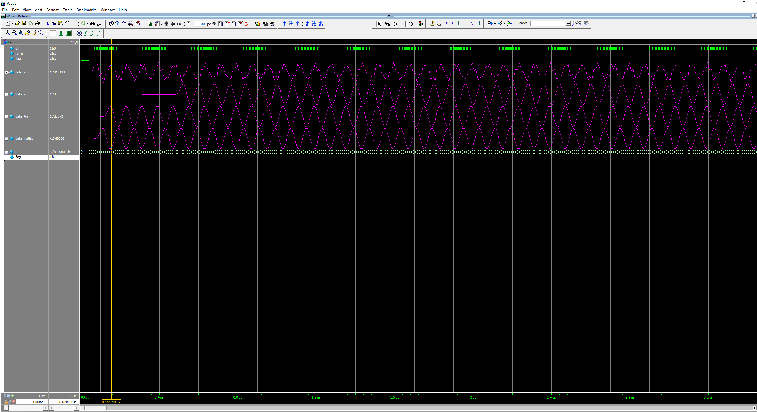
The waveform display results obtained are as follows, from top to bottom are the results of input waveform, 8-bit parallel operation output data, 1-bit serial input data and matlab simulation output data. It can be clearly seen that the waveforms are roughly the same and the filtering effect is good.
In order to accurately verify the completeness of the data, one million groups of data are prepared for the simulation data output comparison test. Use beyond compare to compare, select the difference option and filter out the non difference data. The displayed results are as follows:
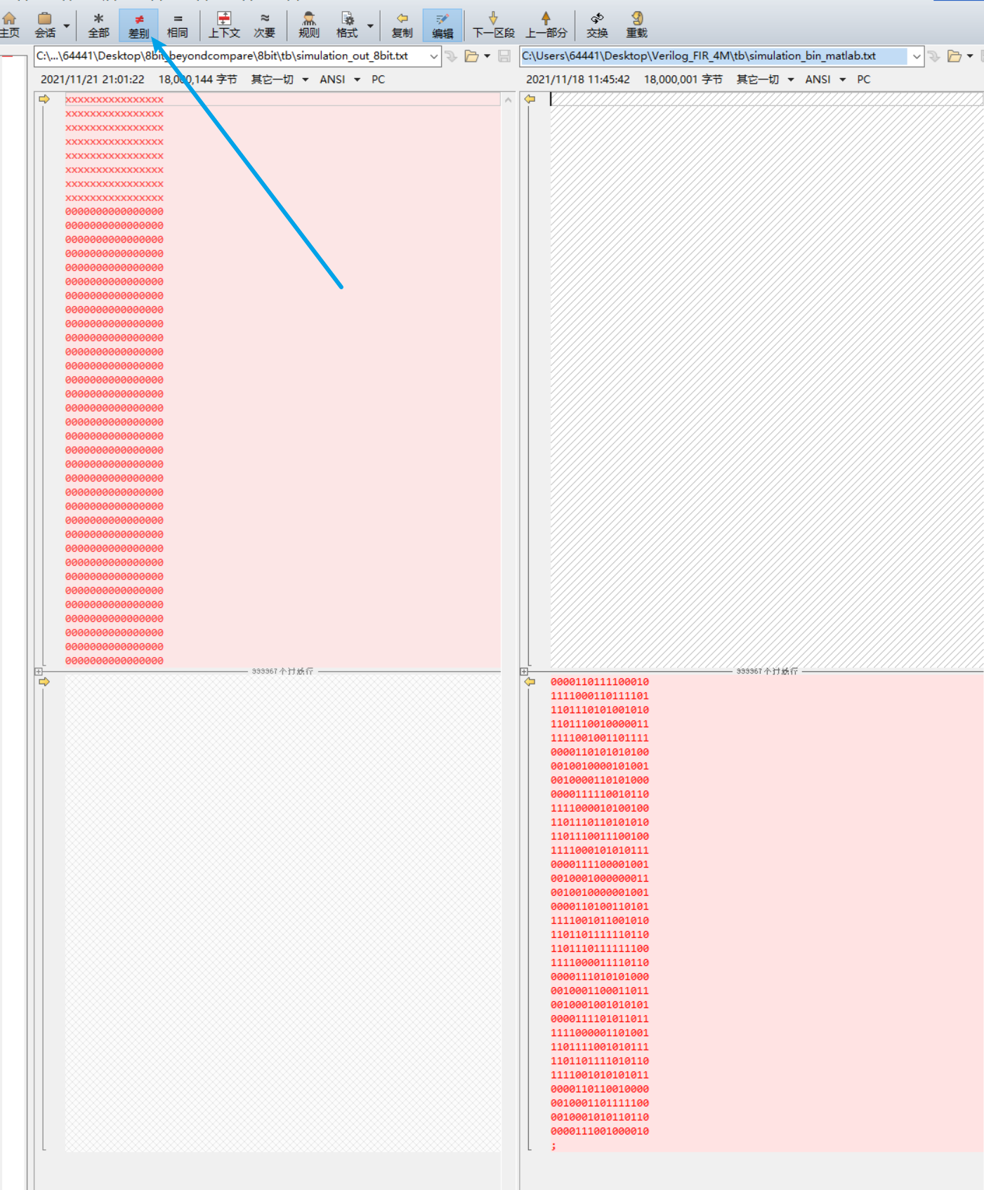
It can be proved that only the first part of the data is different (this is normal due to the different amount of input data). Therefore, the filtering values of the two are completely consistent.
3. Comparison between IIR filter realized by Butterworth filter and Beyond Compare of matlab simulation data
The Beyond Compare comparison method between the IIR filter implemented by Butterworth filter and matlab simulation data is similar to the above method. However, since IIR is a filter with infinite data, the previous filter output results will affect the subsequent data bit output, so the positioning operation is particularly important. Old rule, put the code first:
Top level module:
`timescale 1ns/1ps
//-------------------------------------------------------
//   IIR filter top module
//-------------------------------------------------------
module IIR_top(
    input clk                           ,
    input rst_n                         ,
    input signed [11:0] IIR_input       ,
    output reg signed [11:0] IIR_output
);

parameter U_DLY = 1;//Timing simulation signal, plus u_ Delay of transmission in the circuit of dly analog signal

//-------------------------------------------------------
//   Call zero module
//-------------------------------------------------------
wire signed [20:0] zero_out  ;
wire signed [11:0] pole_in   ;
wire signed [19:0] feedback  ;

//-------------------------------------------------------
//   The input value wave of the waveform is controlled according to the clock signal_ in;
//-------------------------------------------------------
always@(posedge clk or negedge rst_n)
    if(rst_n == 1'b0)begin
        IIR_output <= #U_DLY 12'b0;    // Reset signal, falling edge valid
    end
    else begin
        IIR_output <= #U_DLY pole_in;  // Input waveform data in sequence under the normal periodic signal clk state
    end

zero_module zero
(
    .rst_n (rst_n)             ,
    .clk (clk)                 ,
    .zero_input (IIR_input)    ,
    .zero_output(zero_out)
);

//-------------------------------------------------------
//   Call pole module
//-------------------------------------------------------

pole_module pole
(
    .clk (clk)                  ,
    .rst_n (rst_n)              ,
    .pole_input (pole_in)       ,
    .pole_output(feedback)
);

//-------------------------------------------------------
//   The top-level module calculates the difference and product to form the IIR module
//-------------------------------------------------------
wire signed [20:0] sub_module;

assign sub_module = {zero_out - {feedback[19], feedback}};//The output of the zero point is subtracted from the output of the pole, 21 bits

// assign pole_in = {sub_module[20:9]}  ;// The calculated difference is divided by shift
                                      //The number of bits of the input signal is 12 bits. The number of bits of the output signal is also 12 bits

assign pole_in = {sub_module[20:9]}  ;//The calculated difference is divided by shift


endmodule
Zero module:
`timescale 1ns/1ps
//-------------------------------------------------------
//   IIR filter zero coefficient module
//-------------------------------------------------------

//-------------------------------------------------------
//   Pin module definition
//-------------------------------------------------------
module zero_module(
    input clk                         , //Clock signal clk
    input rst_n                       , //Define a reset signal, which is valid according to the falling edge
    input signed [11:0] zero_input    , //Input of zero module

    output signed [20:0] zero_output    //Output of zero module
);

parameter U_DLY = 1;//Timing simulation signal, plus u_ Delay of transmission in the circuit of dly analog signal

//-------------------------------------------------------
//   The shifted part of the IIR filter successively inputs waves according to the clk clock cycle
//   IIR shape data should also be in rst_ Set to zero when n is 1'b0
//-------------------------------------------------------
reg signed [11:0] data_reg [6:0];

always@(posedge clk or negedge rst_n) begin
    if(rst_n == 1'b0) begin     //Reset signal, the system performs zero setting operation, and the low level of reset signal is effective
        data_reg[0] <= #U_DLY 12'b0   ;
        data_reg[1] <= #U_DLY 12'b0   ;
        data_reg[2] <= #U_DLY 12'b0   ;
        data_reg[3] <= #U_DLY 12'b0   ;
        data_reg[4] <= #U_DLY 12'b0   ;
        data_reg[5] <= #U_DLY 12'b0   ;
        data_reg[6] <= #U_DLY 12'b0   ;
    end
    else
    begin                       //Ordinary clock cycle signal, shift operation in turn, and send new data
        data_reg[6] <= #U_DLY data_reg[5]  ;
        data_reg[5] <= #U_DLY data_reg[4]  ;
        data_reg[4] <= #U_DLY data_reg[3]  ;
        data_reg[3] <= #U_DLY data_reg[2]  ;
        data_reg[2] <= #U_DLY data_reg[1]  ;
        data_reg[1] <= #U_DLY data_reg[0]  ;
        data_reg[0] <= #U_DLY zero_input   ;
    end
end
//-------------------------------------------------------
//   The zeros of IIR filter can be reduced by this way because the coefficients are symmetrical
//   Less devices, add first
//-------------------------------------------------------
wire signed [12:0] add_reg [3:0];

assign add_reg[0] = {zero_input[11], zero_input} + {data_reg[6][11], data_reg[6]}    ;
assign add_reg[1] = {data_reg[0][11], data_reg[0]} + {data_reg[5][11], data_reg[5]}  ;
assign add_reg[2] = {data_reg[1][11], data_reg[1]} + {data_reg[4][11], data_reg[4]}  ;
assign add_reg[3] = {data_reg[2][11], data_reg[2]} + {data_reg[3][11], data_reg[3]}  ;

//-------------------------------------------------------
//   The IIR filter uses the added number for convolution
//-------------------------------------------------------

wire signed [20:0] mult_reg [3:0];
assign mult_reg[0] = {{{6{add_reg[0][12]}}, add_reg[0], 2'b0}
                        + {{8{add_reg[0][12]}}, add_reg[0]}}        ;//*5_101
assign mult_reg[1] = {{{3{add_reg[1][12]}}, add_reg[1], 5'b0}
                        + {{6{add_reg[1][12]}}, add_reg[1], 2'b0}
                        + {{8{add_reg[1][12]}}, add_reg[1]}}        ;//*37_100101
assign mult_reg[2] = {{{2{add_reg[2][12]}}, add_reg[2], 6'b0}
                        + {{3{add_reg[2][12]}}, add_reg[2], 5'b0}
                        + {{5{add_reg[2][12]}}, add_reg[2], 3'b0}
                        + {{6{add_reg[2][12]}}, add_reg[2], 2'b0}
                        + {{7{add_reg[2][12]}}, add_reg[2], 1'b0}}  ;//*110_1101110
assign mult_reg[3] = {{{1{add_reg[3][12]}}, add_reg[3], 7'b0}
                        + {{3{add_reg[3][12]}}, add_reg[3], 5'b0}
                        + {{4{add_reg[3][12]}}, add_reg[3], 4'b0}
                        + {{6{add_reg[3][12]}}, add_reg[3], 2'b0}
                        + {{7{add_reg[3][12]}}, add_reg[3], 1'b0}
                        + {{8{add_reg[3][12]}}, add_reg[3]}}        ;//*183_10110111

//-------------------------------------------------------
//   After convolution, sum and output
//-------------------------------------------------------
assign zero_output = mult_reg[0]
                    + mult_reg[1]
                    + mult_reg[2]
                    + mult_reg[3];

endmodule
Pole module:
`timescale 1ns/1ps
//-------------------------------------------------------
//   IIR filter pole coefficient module
//-------------------------------------------------------

//-------------------------------------------------------
//   Pin module definition
//-------------------------------------------------------

module pole_module(
    input clk                          ,//clock signal
    input rst_n                        ,//Reset signal to enable high level active
    input signed [11:0] pole_input     ,//Input signal

    output signed [19:0] pole_output     //output signal
);

//-------------------------------------------------------
//   Or because the pole module is N-1 bits, we only need 8-1 registers for storage
//   Therefore, a 7-bit reg signal is defined here, and the bandwidth of the signal is the same as that of the input, that is
//   12. Reset signal is cleared; Shift the clk signal;
//-------------------------------------------------------

reg signed [11:0] data_reg [6:0];

always@(posedge clk or negedge rst_n)
    if(rst_n == 1'b0) begin //Reset signal, the system performs zero setting operation, and the low level of reset signal is effective
        data_reg[0] <= 12'd0         ;
        data_reg[1] <= 12'd0         ;
        data_reg[2] <= 12'd0         ;
        data_reg[3] <= 12'd0         ;
        data_reg[4] <= 12'd0         ;
        data_reg[5] <= 12'd0         ;
        data_reg[6] <= 12'd0         ;
    end
    else begin            //Ordinary clock cycle signal, shift operation in turn, and send new data
        data_reg[6] <= data_reg[5]   ;
        data_reg[5] <= data_reg[4]   ;
        data_reg[4] <= data_reg[3]   ;
        data_reg[3] <= data_reg[2]   ;
        data_reg[2] <= data_reg[1]   ;
        data_reg[1] <= data_reg[0]   ;
        data_reg[0] <= pole_input    ;
    end

//-------------------------------------------------------
//   The coefficients of the filter, after quantization, are quantized by 2 ^ 6
//   Multiplication using combinational logic.
//-------------------------------------------------------
wire [19:0] mult_pole [6:0];

assign mult_pole[0] = {{{1{data_reg[1][11]}}, data_reg[1], 7'b0}
                        + {{4{data_reg[1][11]}}, data_reg[1], 4'b0}
                        + {{6{data_reg[1][11]}}, data_reg[1], 2'b0}};//*148_

assign mult_pole[1] = {{{1{data_reg[2][11]}}, data_reg[2], 7'b0}
                        + {{2{data_reg[2][11]}}, data_reg[2], 6'b0}
                        + {{7{data_reg[2][11]}}, data_reg[2], 1'b0}};//*194_

assign mult_pole[2] = {{{1{data_reg[3][11]}}, data_reg[3], 7'b0}
                        + {{4{data_reg[3][11]}}, data_reg[3], 4'b0}
                        + {{5{data_reg[3][11]}}, data_reg[3], 3'b0}
                        + {{8{data_reg[3][11]}}, data_reg[3]}};//*153_

assign mult_pole[3] = {{{2{data_reg[4][11]}}, data_reg[4], 6'b0}
                        + {{5{data_reg[4][11]}}, data_reg[4], 3'b0}
                        + {{6{data_reg[4][11]}}, data_reg[4], 2'b0}
                        + {{7{data_reg[4][11]}}, data_reg[4], 1'b0}
                        + {{8{data_reg[4][11]}}, data_reg[4]}};//*79_

assign mult_pole[4] = {{{4{data_reg[5][11]}}, data_reg[5], 4'b0}
                        + {{5{data_reg[5][11]}}, data_reg[5], 3'b0}
                        + {{7{data_reg[5][11]}}, data_reg[5], 1'b0}};//*26_

assign mult_pole[5] = {{{6{data_reg[6][11]}}, data_reg[6], 2'b0}
                        + {{8{data_reg[6][11]}}, data_reg[6]}};//*5_

assign mult_pole[6] = 20'b0;

//-------------------------------------------------------
//   Convolution sum; Sum all the previous products and set the output to Yout
//   Add the data in the first 7 registers that have completed multiplication
//-------------------------------------------------------
assign pole_output =    {mult_pole[0] +
                        mult_pole[1] +
                        mult_pole[2] +
                        mult_pole[3] +
                        mult_pole[4] +
                        mult_pole[5] +
                        mult_pole[6]};

endmodule
Test file tb:
//~ `New testbench
`timescale  1ns / 1ps

module tb_IIR_top;

// IIR_top Parameters
parameter PERIOD  = 10;


// IIR_top Inputs
reg   clk                             ;
reg   rst_n                           ;
reg   [11:0]  wave_in                 ;

// IIR_top Outputs
wire  [11:0]  wave_out                ;
integer  i                            ;


initial begin
    clk                  = 0          ;
    rst_n                = 0          ;
    wave_in              = 12'd0          ;
    i                    = 0          ;
end

initial
begin
    forever #(PERIOD/2)  clk=~clk;
end

initial
begin
    #(PERIOD*2) rst_n  =  1;
end


parameter DATA_NUM = 32'd10000;
reg [11:0]  data_men[DATA_NUM:1];


initial begin
    $readmemb("C:/Users/64441/Desktop/Verilog_IIR_Butterworth/tb/sin.txt",data_men);   //Pay attention to the direction of the slash, not backward<<<<<<<
end

always @(posedge clk or negedge rst_n) begin //Every CLK_ After the arrival of SIG signal, conduct a data input and input a new waveform data into Din.
    wave_in <= data_men[i];
    i <= i+1;
end


IIR_top  u_IIR_top (
    .clk                     ( clk              ),
    .rst_n                   ( rst_n            ),
    .IIR_input               ( wave_in   [11:0] ),
    .IIR_output              ( wave_out  [11:0] )
);

integer w_file;
initial w_file = $fopen("C:/Users/64441/Desktop/Verilog_IIR_Butterworth/tb/simulation_after_IIR.txt");
always @(i)
begin
    $fdisplay(w_file,"%b",wave_out);
end

endmodule
The simulated pictures are directly displayed in this place:
matlab simulation code of filter:
%Convert binary to decimal data, all data is from sin.txt Export from original file
%%%%%%%%%%%%%%%%%%%%%%%%%%%%%%%%%%%%%%%%%%%%%%%%%%%%%%%%%%%%%%%%%%%%%%%%%%%%%%%%%%%%%%%%%%%%
str_in = importdata('..\tb\sin.txt');
str_length = length(str_in);
str_out = zeros(str_length, 1);
MAX_DATA = 2^11-1;
for number = 1 : str_length
    str_out(number) = bin2dec( num2str(str_in(number)) );
    if(str_out(number) > MAX_DATA)
           str_out(number) = bin2dec( num2str(str_in(number)) ) - 2^12;
    end
end
%%%%%%%%%%%%%%%%%%%%%%%%%%%%%%%%%%%%%%%%%%%%%%%%%%%%%%%%%%%%%%%%%%%%%%%%%%%%%%%%%%%%%%%%%%%%

x_in= str_out;

pole_out = 0;

%Define the initial value of each variable. According to the principle of reset in the circuit, all variables in the convolver are given the initial value
%The size of the initial value is set to 0
x_in_2 = 0;
x_in_3 = 0;
x_in_4 = 0;
x_in_5 = 0;
x_in_6 = 0;
x_in_7 = 0;
x_in_8 = 0;

div = 0;

x_in_6_pole = 0;
x_in_5_pole = 0;
x_in_4_pole = 0;
x_in_3_pole = 0;
x_in_2_pole = 0;
x_in_1_pole = 0;

%Define a matrix array to store our output values
output = zeros(1, str_length);

%Define a binary array storage unit
binary_tem = zeros(1, 12);

%%%%%%%%%%%%%%%%%%%%%%%%%%%%%%%%%%%%%%%%%%%%%%%%%%%%%%%%%%%%%%%%%%%%%%%%%%%%%%%%%%%%%%%%%%%%%%%%%%%%%%%%%%%%%%%%%%%%%%%%%%%%%
for i=1:1:str_length
    %The first convolution operation is the zero point operation
     %Convolution operation, convolute the data in the original register, and put the convoluted data into y Yes.
     y = x_in(i)*5 + x_in_2 * 37 + x_in_3 * 110 +  x_in_4 * 183 + x_in_5 * 183 + x_in_6 * 110 + x_in_7 * 37 + x_in_8 * 5;

     %Move the data in turn
     x_in_8 = x_in_7;
     x_in_7 = x_in_6;
     x_in_6 = x_in_5;
     x_in_5 = x_in_4;
     x_in_4 = x_in_3;
     x_in_3 = x_in_2;
     x_in_2 = x_in(i);

     %The second convolution operation is the pole operation
     %Convolution operation, the convoluted value is calculated and placed in pole in
     pole = x_in_1_pole * 148 + x_in_2_pole * 194 + x_in_3_pole * 153 +  x_in_4_pole * 79 + x_in_5_pole * 26 + x_in_6_pole * 5;

     %Move the data in turn
     x_in_6_pole = x_in_5_pole;
     x_in_5_pole = x_in_4_pole;
     x_in_4_pole = x_in_3_pole;
     x_in_3_pole = x_in_2_pole;
     x_in_2_pole = x_in_1_pole;
     x_in_1_pole = div;

     %The subtraction of data is equivalent to the difference between the operation value of zero point and the operation value of pole
     sub = y - pole;
     %It is equivalent to the data truncation operation. Due to the need for truncation division, the original 21 bit data only needs to get a 12 bit value by simulating the data truncation operation
     %Therefore, only reading the data of the first twelve bits is equivalent to intercepting the data of the last nine bits
        B_s=dec2bin(sub+((sub)<0)*2^21,21);
        for j=1:12
          if B_s(j)=='1'
              binary_tem(1, j) = 1;
          else
              binary_tem(1, j) = 0;
          end
        end

        if(binary_tem(1, 1) == 0)
            div = binary_tem(1, 1) * 2048 + binary_tem(1, 2) * 1024 + binary_tem(1, 3) * 512 + binary_tem(1, 4) * 256 + binary_tem(1, 5) * 128 + binary_tem(1, 6) * 64 + binary_tem(1, 7) * 32 + binary_tem(1, 8) * 16 + binary_tem(1, 9) * 8 + binary_tem(1, 10) * 4 + binary_tem(1, 11) * 2 + binary_tem(1, 12) * 1;
        else
            div =  ~(binary_tem(1, 1)) * 2048 +  ~(binary_tem(1, 2)) * 1024 + ~(binary_tem(1, 3)) * 512 + ~(binary_tem(1, 4)) * 256 + ~(binary_tem(1, 5)) * 128 + ~(binary_tem(1, 6)) * 64 + ~(binary_tem(1, 7)) * 32 + ~(binary_tem(1, 8)) * 16 + ~(binary_tem(1, 9)) * 8 + ~(binary_tem(1, 10)) * 4 + ~(binary_tem(1, 11)) * 2 + ~(binary_tem(1, 12)) * 1;
            div = div + 1;
            div = -div;
        end


    %get div The value after truncation is put into the output matrix output(1, i)Middle go
    output(1, i) = div;
end
%%%%%%%%%%%%%%%%%%%%%%%%%%%%%%%%%%%%%%%%%%%%%%%%%%%%%%%%%%%%%%%%%%%%%%%%%%%%%%%%%%%%%%%%%%%%%%%%%%%%%%%%%%%%%%%%%%%%%%%%%%%%%

%The data writing of waveform data outputs the data after truncation, that is, the output filtered waveform data
fid = fopen('..\tb\simulation_MATLAB_IIR.txt','w');
for k=1:length(output)
    B_s=dec2bin(output(k)+((output(k))<0)*2^12,12);
    for j=1:12
       if B_s(j)=='1'
           tb=1;
       else
           tb=0;
       end
       fprintf(fid,'%d',tb);
    end
    fprintf(fid,'\r\n');
end
fprintf(fid,';');
fclose(fid);
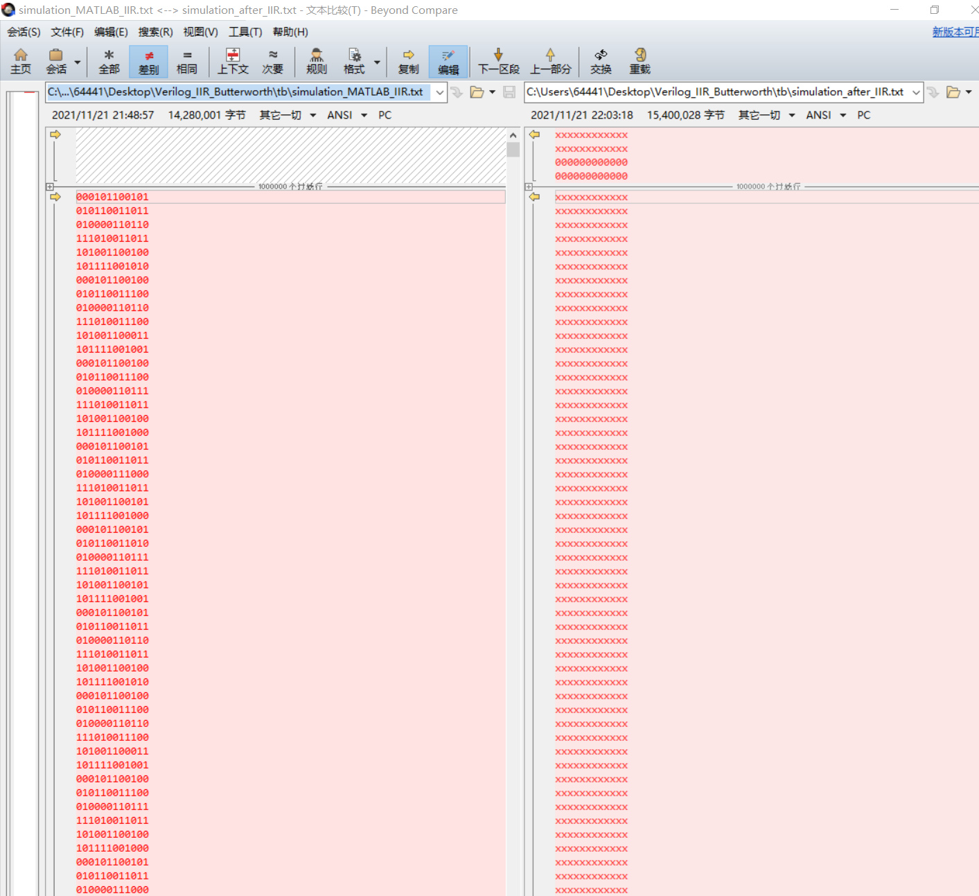
The matalb simulation data is compared with the FPGA simulation data to verify the correctness of the filtering results of the Butterworth filter. After comparison with Beyond Compare and selecting the difference option, it can be seen that except for the difference between the beginning and the end, the other data are the same. So the data matches.