1) Experimental platform: ZYNQ development board of punctual atomic navigator
2) Platform purchase address: https://item.taobao.com/item.htm?&id=606160108761
3) Full set of experimental source code + manual + video download address: http://www.openedv.com/thread-301505-1-1.html
4) Students interested in punctual atomic FPGA can add group discussion: 994244016
5) pay attention to the official account of the dot atom and get updated information.

Chapter 36 PL Ethernet video transmission experiment based on OV5640
Like OV7725, OV5640 is a CMOS image sensor produced by OmniVision (Howell Technology). The difference is that OV5640 supports higher resolution, acquisition rate and higher image processing performance. It is mainly used in mobile phones, digital cameras, computer multimedia and other fields.
In the "PL Ethernet video transmission experiment based on OV7725", we successfully displayed the images collected by the camera in real time on the host computer display software. In this chapter, we will use the ZYNQ development board to realize the digital image acquisition of OV5640, and send it to the host computer for real-time display through the PL Ethernet interface on the development board.
This chapter is divided into the following chapters:
36.1 introduction
36.2 experimental tasks
36.3 hardware design
36.4 program design
36.5 download verification
36.1 introduction
OV5640 is a 1 / 4-inch single-chip image sensor. Its photosensitive array reaches 25921944 (i.e. 500W pixels), which can realize the fastest image acquisition with 15fps QSXVGA (25921944) or 90fps VGA (640 * 480) resolution. The sensor adopts OmniBSI (back illumination) technology introduced by OmniVision to achieve higher performance, such as high sensitivity, low crosstalk and low noise. Image processing functions are integrated in the sensor, including automatic exposure control (AEC), automatic white balance (AWB), etc. At the same time, the sensor supports LED lighting, MIPI (mobile industry processor interface) output interface and DVP (digital video parallel) output interface selection, ISP (image signal processing) and AFC (automatic focus control).
The functional block diagram of OV5640 is shown in the following figure:
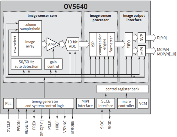
Figure 7.5.13.1 OV5640 function block diagram
It can be seen from the above figure that the timing generator controls the image array, amplifier (AMP), AD conversion and outputs external timing signals (VSYNC, HREF and PCLK). The clock output by the external clock XVCLK after passing through the PLL phase-locked loop is used as the control clock of the system; The photosensitive array converts the optical signal into an analog signal and enters the 10 bit AD converter after passing through the gain amplifier; The AD converter converts the analog signal into digital signal, carries out relevant image processing through ISP, and finally outputs the 10 bit video data stream in the configured format. Gain amplifier control and ISP can be configured through registers. The interface of configuration register is SCCB interface, and the interface protocol is compatible with IIC protocol.
OV5640 uses a two-wire SCCB interface bus. For details of SCCB bus, please refer to the introduction of OV7725 in "PL Ethernet video transmission experiment based on OV7725". Although both OV5640 and OV7725 use SCCB interface bus to configure registers, the difference is that OV7725 uses 8 bits (1 byte) to represent the register address, while OV5640 uses 16 bits (2 bytes) to represent the register address.
The write transmission protocol of OV5640 SCCB is shown in the figure below:
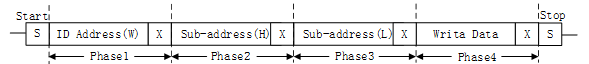
Figure 7.5.13.2 OV5640 SCCB write transfer protocol
The ID address in the above figure is composed of a 7-bit device address and a 1-bit read-write control bit (0: write, 1: read). The device address of OV5640 is 7'h3c, so in the write transmission protocol, ID address (W) = 8'h78 (the device address is shifted by 1 bit to the left and the low bit is supplemented by 0); Sub address (H) is the high 8-bit register address and sub address (L) is the low 8-bit register address. Among the OV5640 registers, some are rewritable and some are read-only. Only rewritable registers can be written correctly; Write Data is 8-bit Write Data, and each register address corresponds to 8-bit configuration data.
Before the OV5640 works normally, the sensor must be initialized, that is, make it work in the expected working mode through the configuration register and get a better image quality. Because the write transfer protocol of SCCB is almost the same as that of IIC, we can directly use the driver of IIC to configure the camera. Of course, not all of these registers need to be configured. Many registers can adopt default values. OV company provided the software application manual of OV5640 (OV5640 Software Application Note, located in the data "7_ hardware data / 4_OV5640 data / OV5640_camera_module_software_application_notes.pdf" attached to the development board). If you do not know how to configure some registers, you can refer to this manual. The following table is the configuration description of key registers used in this program.
Table 36.1.1 OV5640 key register configuration description
address
(HEX) register default
(HEX) detailed description
0x3008 SYSTEM CTROL0 0x02 Bit[7]: software reset
Bit[6]: software power sleep
0x3016 PAD OUTPUT ENABLE 00 0x00 Bit[1]: flash output enable
0x3017 PAD OUTPUT ENABLE 01 0x00 input / output control (0: input 1: output)
Bit[7]: FREX output enable
Bit[6]: VSYNC output enable
Bit[5]: HREF output enable
Bit[4]: PCLK output enable
Bit[3:0]: D[9:6] output enable
0x3018 PAD OUTPUT ENABLE 02 0x00 input / output control (0: input 1: output)
Bit[7:2]: D[5:0] output enable
Bit[1]: GPIO1 output enable
Bit[0]: GPIO0 output enable
0x3019 PAD OUTPUT VALUE 00 0x00 Bit[1]: flash operation
0: turn off the flash
1: Turn on the flash
0x301C PAD SELECT 00 0x00 Bit[1]: Flash IO selection
0x3035 SC PLL CONTRL1 0x11 Bit[7:4]: system clock frequency division, used to reduce all clock frequencies
Bit[3:0]: MIPI frequency division
0x3036 SC PLL CONTRL2 0x69 Bit[7:0]:PLL frequency multiplier (4 ~ 252)
Any integer frequency division is supported in the range of 4 ~ 127
Only even frequency division is supported in the range of 128 ~ 252
0x3808 TIMING DVPHO 0x0A Bit[3:0]: 4 bits higher than the number of horizontal pixels of DVP output
0x3809 TIMING DVPHO 0x20 Bit[7:0]: 8 bits lower than the number of horizontal pixels of DVP output
0x380A TIMING DVPVO 0x07 Bit[2:0]: the number of vertical pixels of DVP output is 3 bits higher
0x380B TIMING DVPVO 0x98 Bit[7:0]: 8 bits lower than the number of output vertical pixels
0x4300 FORMAT CONTROL 0xF8 Bit[7:4]: data output format
0: RAW
1: Y8
2: YUV444/RGB888
3: YUV422
4: YUV420
5: YUV420 (valid only at MIPI output interface)
6: RGB565
Bit[3:0]: output sequence
0: {b[4:0],g[5:3]},{g[2:0],r[4:0]}
1: {r[4:0],g[5:3]},{g[2:0],b[4:0]}
2: {g[4:0],r[5:3]},{r[2:0],b[4:0]}
3: {b[4:0],r[5:3]},{r[2:0],g[4:0]}
4: {g[4:0],b[5:3]},{b[2:0],r[4:0]}
5: {r[4:0],b[5:3]},{b[2:0],g[4:0]}
6 ~ 14: not allowed
15: {g[2:0],b[4:0]},{r[4:0],g[5:3]}
7: RGB555 format 1
8: RGB555 format 2
9: RGB444 format 1
10: RGB444 format 2
11 ~ 14: not allowed
15: Bypass formatter module
Ov5640 has many registers. For descriptions of other registers, please refer to the data manual of ov5640. It should be noted that the data manual of ov5640 does not provide all register descriptions, and most of the necessary register configurations can be found in the software application manual of ov5640. You can learn how to configure ov5640 by combining these two manuals.
Output image parameter setting
Next, let's introduce the ISP input window settings, pre zoom window settings and output size window settings of OV5640. These settings are closely related to our normal use. It is necessary to understand their setting relationship, as shown in the following figure:
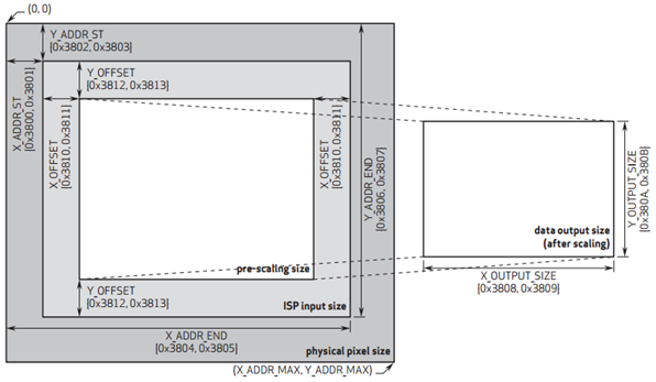
Figure 7.5.13.3 image window setting
ISP Input Size allows the user to set the whole sensor display area (physical pixel size, 26321951, in which 25921944 pixels are valid), and the window opening range can be set arbitrarily from 00 to 26321951. That is, the X in the figure above_ ADDR_ St (register address 0x3800, 0x3801), Y_ADDR_ST (register address 0x3802, 0x3803), X_ADDR_END (register address 0x3804, 0x3805) and Y_ADDR_END (register address 0x3806, 0x3807) register. The pixel data in the setting range of this window will enter the ISP for image processing.
Pre scaling size allows the user to crop based on the ISP input window. It is used to set the size of the window to be scaled. This setting only offsets the X/Y direction in the ISP input window. You can use X_OFFSET (register addresses 0x3810, 0x3811) and Y_OFFSET (register addresses 0x3812, 0x3813) is configured.
Data output size window setting (data output size) is based on the pre scaling window, which is scaled by the internal DSP, and the processed data is output to the external image window, which controls the final image output size. You can use X_OUTPUT_SIZE (register address 0x3808, 0x3809) and Y_OUTPUT_SIZE (register addresses 0x380A, 0x380B). Note: when the scale of the output size window is inconsistent with that of the pre scaling window, the image will be scaled (image deformation). Only when the scale of the two is consistent, the output scale is 1:1 (normal image).
In figure 7.5.13.3, the data output size area on the right is the image size output by OV5640 to the outside, that is, the image size displayed on the display or LCD. When the scale of the output size window is inconsistent with that of the pre scaling window, scaling processing will be carried out, and the image seen on the display will be deformed.
Output pixel format
OV5640 supports a variety of different data pixel formats, including YUV (pixel format represented separately by luminance parameters and chroma parameters), RGB (where RGB format includes RGB565, RGB555, etc.) and RAW (original image data). Different data pixel formats are configured through register address 0x4300.
Since RGB565 is commonly used for data pixel format, we also configure ov5640 as RGB565 format here. As can be seen from the above table (table 36.1.1), set Bit[7:4] of register 0x4300 to 0x6. Ov5640 supports adjusting the order of color variables in RGB565 output format. For our common applications, RGB or BGR sequences are generally used. We introduced in the chapter of "PL Ethernet video transmission experiment based on OV7725". The OV7725 camera outputs in RGB order. In this chapter, we keep the color order of RGB565 output by ov5640 consistent with OV7725, and set the Bit[3:0] of register 0x4300 to 0x1. Therefore, the image acquisition module in the chapter "PL Ethernet video transmission experiment based on OV7725" can be directly used to acquire the image output by ov5640.
Color bar test mode
After the image sensor is configured into the color bar test mode, it will output color stripes to test whether the image sensor works normally. Turn on and off the color bar mode through the Bit[7] bit of the configuration register 0x503d. When the color bar mode needs to be turned on, the register 0x503d is configured as 0x80 and 0x00 when it is turned off. The following figure shows the stripes of the image output after the color bar mode is turned on.

Figure 7.5.13.4 image stripes in color bar mode
LED flash
When the external ambient light is dark, the image collected by the sensor will be greatly affected. At this time, you can turn on the LED fill light to make up for the impact caused by insufficient illumination, just as the mobile phone will turn on the flash when taking pictures at night to improve the image quality. Enable the LED fill light function by configuring registers 0x3016=0x02, 0x301c=0x02; The configuration register 0x3019=0x02 turns on the flash and 0x3019=0x00 turns off the flash.
Image output timing
Next, we introduce the image data output timing of OV5640. First, we briefly introduce some definitions.
QSXGA here refers to the output format with a resolution of 25921944. Similar formats include QXGA(20481536), UXGA(16001200), SXGA(12801024), WXGA(1440900), WXGA(1280800), XGA(1024768), SVGA(800600), VGA(640480), QVGA(320240) and QQVGA(160120).
PCLK: pixel clock. A PCLK clock outputs one pixel or half a pixel (high 8 bits or low 8 bits of pixel data).
VSYNC: frame synchronization signal.
HREF/HSYNC: line synchronization signal.
D[9:0]: pixel data. In RGB565 format, only the upper 8 bits are valid.
tPclk: one clock cycle.
tp: the period of one pixel, tp=2tPclk in RGB565 and YUV422 output formats; In Raw output format, tp=tPclk.
The following figure is a line timing diagram of OV5640 output image data.

Figure 7.5.13.5 OV5640 line sequence diagram
As can be seen from the above figure, the sensor outputs image data when the HREF is high. When the HREF becomes high, each PCLK clock outputs an 8-bit or 10 bit pixel data. For example, we use QSXGA timing, RGB565 format output, tp=2tPclk, and every two bytes form the color of a pixel, so that a total of 25922 pclks, that is, 25922 bytes, are output per line.
Let's look at the frame timing (QSXGA mode, resolution 25921944), as shown in the following figure:
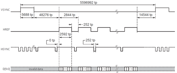
Figure 7.5.13.6 OV5640 QSXGA frame timing
It can be seen from the above figure that the rising edge of VSYNC is the beginning of a frame, and the time of high-level synchronization pulse is 5688tp. Then, after waiting for 48276tp, HREF starts to pull up, and valid data is output at this time; HREF consists of 2592tp high levels and 252tp low levels; After the output of the last line of image data is completed, wait for 14544tp time, and one frame data transmission ends. Therefore, the time of outputting one frame of image is actually tFrame = 5596992tp.
From the line timing diagram and frame timing diagram of OV5640, it can be found that its output timing is very similar to OV7725, but the time parameters are different. You can refer to the introduction of frame timing in "PL Ethernet video transmission experiment based on OV7725" to learn the output timing of OV5640.
36.2 experimental tasks
The experimental task of this section is to use ZYNQ development board and OV5640 camera to realize image acquisition, and send it to the host computer for real-time display through the Ethernet interface on the development board.
36.3 hardware design
The hardware circuit of this experiment is basically the same as that in the "PL Ethernet video transmission experiment based on OV7725". Both use the camera expansion interface on the pilot Zynq development board, and the configuration of IO pin position is the same.
The only difference is that the "cam_sgm_ctrl" signal originally output by Zynq to the camera extension interface in the "PL Ethernet video transmission experiment based on OV7725" has changed into the "power sleep mode selection" signal cam output by Zynq to OV5640 in this experiment_ pwdn; And the original cam_ sgm_ CTRL is that we need to always assign it to high level, but for OV5640, cam_pwdn we need to assign it to the low level all the time, which means that it is not dormant, that is, the normal working mode.
The pin assignment of OV5640 camera is shown in the following table:
Table 36.3.1 OV5640 camera pin assignment
Signal name direction pin port description
cam_pclk input W14 cmos data pixel clock
cam_vsync input U12 cmos field synchronization signal
cam_href input T12 cmos line sync signal
cam_rst_n output P14 cmos reset signal, active at low level
cam_pwdn output V15 cmos power sleep mode selection signal
cam_data[0] input R14 cmos data
cam_data[1] input U13 cmos data
cam_data[2] input V13 cmos data
cam_data[3] input U15 cmos data
cam_data[4] input U14 cmos data
cam_data[5] input W13 cmos data
cam_data[6] input V12 cmos data
cam_data[7] input Y14 cmos data
emio_sccb_tri_io [0] inout T10 cmos SCCB_SCL line
emio_sccb_tri_io [1] inout T11 cmos SCCB_SDA line
The related pin constraints are as follows:
create_clock -period 20.000 -name sys_clk [get_ports sys_clk]
create_clock -period 8.000 -name eth_rxc [get_ports eth_rxc]
set_property -dict {PACKAGE_PIN U18 IOSTANDARD LVCMOS33} [get_ports sys_clk]
set_property -dict {PACKAGE_PIN N16 IOSTANDARD LVCMOS33} [get_ports sys_rst_n]

set_property -dict {PACKAGE_PIN G15 IOSTANDARD LVCMOS33} [get_ports eth_rst_n]
set_property -dict {PACKAGE_PIN K17 IOSTANDARD LVCMOS33} [get_ports eth_rxc]
set_property -dict {PACKAGE_PIN E17 IOSTANDARD LVCMOS33} [get_ports eth_rx_ctl]
set_property -dict {PACKAGE_PIN B19 IOSTANDARD LVCMOS33} [get_ports {eth_rxd[0]}]
set_property -dict {PACKAGE_PIN A20 IOSTANDARD LVCMOS33} [get_ports {eth_rxd[1]}]
set_property -dict {PACKAGE_PIN H17 IOSTANDARD LVCMOS33} [get_ports {eth_rxd[2]}]
set_property -dict {PACKAGE_PIN H16 IOSTANDARD LVCMOS33} [get_ports {eth_rxd[3]}]

set_property -dict {PACKAGE_PIN B20 IOSTANDARD LVCMOS33} [get_ports eth_txc]
set_property -dict {PACKAGE_PIN K18 IOSTANDARD LVCMOS33} [get_ports eth_tx_ctl]
set_property -dict {PACKAGE_PIN D18 IOSTANDARD LVCMOS33} [get_ports {eth_txd[0]}]
set_property -dict {PACKAGE_PIN C20 IOSTANDARD LVCMOS33} [get_ports {eth_txd[1]}]
set_property -dict {PACKAGE_PIN D19 IOSTANDARD LVCMOS33} [get_ports {eth_txd[2]}]
set_property -dict {PACKAGE_PIN D20 IOSTANDARD LVCMOS33} [get_ports {eth_txd[3]}]

#CAMERA
create_clock -period 40.000 -name cmos_pclk [get_ports cam_pclk]
set_property CLOCK_DEDICATED_ROUTE FALSE [get_nets cam_pclk_IBUF]
set_property -dict {PACKAGE_PIN W14 IOSTANDARD LVCMOS33} [get_ports cam_pclk]
set_property -dict {PACKAGE_PIN P14 IOSTANDARD LVCMOS33} [get_ports cam_rst_n]
set_property -dict {PACKAGE_PIN V15 IOSTANDARD LVCMOS33} [get_ports cam_sgm_ctrl]
set_property -dict {PACKAGE_PIN R14 IOSTANDARD LVCMOS33 IOB TRUE} [get_ports {cam_data[0]}]
set_property -dict {PACKAGE_PIN U13 IOSTANDARD LVCMOS33 IOB TRUE} [get_ports {cam_data[1]}]
set_property -dict {PACKAGE_PIN V13 IOSTANDARD LVCMOS33 IOB TRUE} [get_ports {cam_data[2]}]
set_property -dict {PACKAGE_PIN U15 IOSTANDARD LVCMOS33 IOB TRUE} [get_ports {cam_data[3]}]
set_property -dict {PACKAGE_PIN U14 IOSTANDARD LVCMOS33 IOB TRUE} [get_ports {cam_data[4]}]
set_property -dict {PACKAGE_PIN W13 IOSTANDARD LVCMOS33 IOB TRUE} [get_ports {cam_data[5]}]
set_property -dict {PACKAGE_PIN V12 IOSTANDARD LVCMOS33 IOB TRUE} [get_ports {cam_data[6]}]
set_property -dict {PACKAGE_PIN Y14 IOSTANDARD LVCMOS33 IOB TRUE} [get_ports {cam_data[7]}]
set_property -dict {PACKAGE_PIN U12 IOSTANDARD LVCMOS33} [get_ports cam_vsync]
set_property -dict {PACKAGE_PIN T12 IOSTANDARD LVCMOS33} [get_ports cam_href]
set_property -dict {PACKAGE_PIN T10 IOSTANDARD LVCMOS33} [get_ports cam_scl]
set_property -dict {PACKAGE_PIN T11 IOSTANDARD LVCMOS33} [get_ports cam_sda]
36.4 program design
Figure 7.5.13.1 is the system block diagram drawn according to the experimental tasks in this chapter. Comparing the system block diagram of "Ethernet video transmission experiment based on OV7725", it can be found that we only replaced the peripheral OV7725 module with OV5640 module, and the other modules are basically the same (IIC configuration modules are different). The clock IP core module is used to provide drive clock for IIC drive module, Ethernet top-level module and start transmission control module. The I2C driving module and I2C configuration module are used to initialize the OV5640 image sensor; The camera acquisition module is responsible for collecting the camera image data and connecting the image data to the image data packaging module. The image data packaging module splices the input image data and adds the frame header and line field resolution of the image; The Ethernet top-level module realizes the sending and receiving of Ethernet data; The start transmission control module controls the Ethernet top-level module to start / stop sending data.
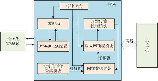
Figure 7.5.13.1 system block diagram
The schematic diagram of the top-level module is shown in the figure below:
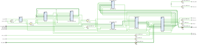
Figure 7.5.13.2 schematic diagram of top-level module
The FPGA top-level module (ov5640_udp_pc) instantiates the following seven modules: clock IP core module (clk_wiz_0), I2C drive module (i2c_dri), I2C configuration module (i2c_ov5640_rgb565_cfg), camera image acquisition module (cmos_capture_data), start_transfer_ctrl Image data encapsulation module (img_data_pkt) and Ethernet top module (eth_top).
Clock module (clk_wiz_0): the clock IP core module is realized by calling the MMCM IP core. A total of 2 clocks are output with frequencies of 50Mhz and 200Mhz respectively. 50Mhz clock is used as the operation clock of IIC drive module; The 200Mhz clock is used as the reference clock of the source language of idlayctrl.
I2C driver module (i2c_dri): I2C driver module is responsible for driving the OV5640 SCCB interface bus. Users can easily configure the registers of OV5640 according to the user interface provided by the module. This module is the same module as the I2C driver module used in the chapter "EEPROM reading and writing experiment", For the detailed introduction of this module, please refer to the chapter "EEPROM reading and writing experiment".
I2C configuration module (i2c_ov5640_rgb565_cfg): the driving clock of I2C configuration module is provided by the clock output by I2C driving module, which facilitates the data interaction between I2C driving module and I2C configuration module. The module registers the register address, data to be configured and the start and end of control initialization. At the same time, the module outputs the register address and data of OV5640 and the control signal to control the I2C drive module to start execution, which is directly connected to the user interface of I2C drive module, so as to complete the initialization of OV5640 sensor.
cmos_capture_data: driven by the pixel clock, the camera acquisition module converts the field synchronization signal, line synchronization signal and 8-bit data output by the sensor into 16 bit data signal to complete the image acquisition of OV5640 sensor.
start_transfer_ctrl: This module parses the data received by the Ethernet top-level module. If 1 byte ASCII code "1" is received, it indicates that the Ethernet starts transmitting image data; If 1 byte ASCII code "0" is received, it means that Ethernet stops transmitting image data.
Image data encapsulation module (img_data_pkt): the image data encapsulation module is responsible for splicing the input 16 bit image data into 32-bit data, and adding the frame header and line field resolution of the image data. The module controls the number of bytes sent by the Ethernet sending module and the number of bytes of one line of image data sent at a time. An asynchronous FIFO module is instantiated in the module to cache the image data to be sent.
Ethernet top module (eth_top): the Ethernet top module realizes the sending and receiving function of Ethernet communication. For a detailed introduction of this module, please refer to the chapter "Ethernet UDP test experiment".
The top-level module code is as follows:
1   module ov5640_udp_pc(
2       input              sys_clk     ,   //System clock
3       input              sys_rst_n   ,   //System reset signal, active at low level
4       //Ethernet interface
5       input              eth_rxc     ,   //RGMII receive data clock
6       input              eth_rx_ctl  ,   //RGMII input data valid signal
7       input       [3:0]  eth_rxd     ,   //RGMII input data
8       output             eth_txc     ,   //RGMII transmit data clock
9       output             eth_tx_ctl  ,   //RGMII output data valid signal
10      output      [3:0]  eth_txd     ,   //RGMII output data
11      output             eth_rst_n   ,   //Ethernet chip reset signal, low level effective
12
13      //Camera interface
14      input              cam_pclk     ,  //cmos data pixel clock
15      input              cam_vsync    ,  //cmos field synchronization signal
16      input              cam_href     ,  //cmos line synchronization signal
17      input   [7:0]      cam_data     ,  //cmos data
18      output             cam_rst_n    ,  //cmos reset signal, active at low level
19      output             cam_pwdn     ,  //Power sleep mode selection 0: normal mode 1: power sleep mode
20      output             cam_scl      ,  //cmos SCCB_SCL line
21      inout              cam_sda         //cmos SCCB_SDA line
22  );
23
24  //parameter define
25  //Development board MAC address 00-11-22-33-44-55
26  parameter  BOARD_MAC = 48'h00_11_22_33_44_55;
27  //Development board IP address 192.168.1.10
28  parameter  BOARD_IP  = {8'd192,8'd168,8'd1,8'd10};
29  //Destination MAC address ff_ff_ff_ff_ff_ff
30  parameter  DES_MAC   = 48'hff_ff_ff_ff_ff_ff;
31  //Destination IP address 192.168.1.102
32  parameter  DES_IP    = {8'd192,8'd168,8'd1,8'd102};
33
34  parameter  H_CMOS_DISP = 11'd640;                  //CMOS resolution - row
35  parameter  V_CMOS_DISP = 11'd480;                  //CMOS resolution - columns
36  parameter  TOTAL_H_PIXEL = H_CMOS_DISP + 12'd1216; //Total horizontal pixel size
37  parameter  TOTAL_V_PIXEL = V_CMOS_DISP + 12'd504;  //Total vertical pixel size
38
39  parameter SLAVE_ADDR = 7'h3c          ; //Device address 7'h3c of OV5640
40  parameter BIT_CTRL   = 1'b1           ; //The byte address of OV5640 is 16 bits 0:8 bits 1:16 bits
41  parameter CLK_FREQ   = 27'd50_000_000 ; //i2c_ Drive clock frequency of DRI module
42  parameter I2C_FREQ   = 20'd250_000    ; //SCL clock frequency of I2C, not exceeding 400KHz
Four parameters are defined in lines 24 to 32 of the code: MAC address board of the development BOARD_MAC, development board IP address BOARD_IP, destination MAC address DES_MAC (here refers to PC MAC address), destination IP address DES_IP (PC IP address). The MAC address and IP address of the development board are defined at will, as long as they are not the same as the destination MAC address and destination IP address, otherwise address conflicts will occur. The destination MAC address here is the public MAC address (48'hff_ff_ff_ff_ff_ff_ff), which can also be modified to the MAC address of the computer network interface, DES_IP is the IP address corresponding to the computer Ethernet. The four parameters defined here are passed down. If you need to modify the MAC address or IP address, you can modify it directly here instead of in the Ethernet top-level module.
Lines 34 to 37 of the code define the number of CMOS horizontal / vertical pixels and the total number of horizontal / vertical pixels. The camera resolution set in this experiment is 640 * 480.
The device address of OV5640 is defined in line 39 of the code, and its device address is 7'h3c; Line 40 defines the bit width of the register address, BIT_CTRL=0 indicates that the address bit width is 8 bits, BIT_CTRL=1 indicates that the address bit width is 16 bits. Because the address bit width of OV5640 is 16 bits, BIT_CTRL is set to 1.
76  assign  rst_n = sys_rst_n & locked;
77  //Power sleep mode selection 0: normal mode 1: power sleep mode
78  assign  cam_pwdn  = 1'b0;
79  assign  cam_rst_n = 1'b1;
80
81  //Instantiated clock IP core
82  clk_wiz_0 u_clk_wiz_0
83     (
84      .clk_out1    (clk_50m),
85      .clk_out2    (clk_200m),
86      .reset       (~sys_rst_n),
87      .locked      (locked),
88      .clk_in1     (sys_clk)
89      );
90
91  //I2C configuration module
92  i2c_ov5640_rgb565_cfg u_i2c_cfg(
93      .clk           (i2c_dri_clk),
94      .rst_n         (rst_n),
95      .i2c_done      (i2c_done),
96      .i2c_data_r    (i2c_data_r),
97      .cmos_h_pixel  (H_CMOS_DISP),
98      .cmos_v_pixel  (V_CMOS_DISP),
99      .total_h_pixel (TOTAL_H_PIXEL),
100     .total_v_pixel (TOTAL_V_PIXEL),
101     .i2c_exec      (i2c_exec),
102     .i2c_data      (i2c_data),
103     .i2c_rh_wl     (i2c_rh_wl),
104     .init_done     (cam_init_done)
105     );
106
107 //I2C drive module
108 i2c_dri
109    #(
110     .SLAVE_ADDR  (SLAVE_ADDR),               //Parameter transfer
111     .CLK_FREQ    (CLK_FREQ  ),
112     .I2C_FREQ    (I2C_FREQ  )
113     )
114    u_i2c_dri(
115     .clk         (clk_50m   ),
116     .rst_n       (rst_n     ),
117     //i2c interface
118     .i2c_exec    (i2c_exec  ),
119     .bit_ctrl    (BIT_CTRL  ),
120     .i2c_rh_wl   (i2c_rh_wl ),
121     .i2c_addr    (i2c_data[23:8]),
122     .i2c_data_w  (i2c_data[7:0]),
123     .i2c_data_r  (i2c_data_r),
124     .i2c_done    (i2c_done  ),
125     .i2c_ack     (),
126     .scl         (cam_scl   ),
127     .sda         (cam_sda   ),
128     //user interface
129     .dri_clk     (i2c_dri_clk)               //I2C operation clock
130 );
131
132 //Camera data acquisition module
133 cmos_capture_data u_cmos_capture_data(
134
135     .rst_n              (rst_n & cam_init_done),
136     .cam_pclk           (cam_pclk),
137     .cam_vsync          (cam_vsync),
138     .cam_href           (cam_href),
139     .cam_data           (cam_data),
140     .cmos_frame_vsync   (cmos_frame_vsync),
141     .cmos_frame_href    (),
142     .cmos_frame_valid   (img_data_en),
143     .cmos_frame_data    (img_data)
144     );
The OV5640 camera configuration module and IIC driver module initialize the OV5640 camera and pull up the cam after initialization_ init_ Done signal, at this time, start to receive the image data output by the camera through the camera data acquisition module (as shown in the code in line 135 of the program), and convert the input 8-bit data into 16 bit RGB565 data.
146 //Start transmission of control module
147 start_transfer_ctrl u_start_transfer_ctrl(
148     .clk                (eth_rx_clk),
149     .rst_n              (rst_n),
150     .udp_rec_pkt_done   (udp_rec_pkt_done),
151     .udp_rec_en         (udp_rec_en      ),
152     .udp_rec_data       (udp_rec_data    ),
153     .udp_rec_byte_num   (udp_rec_byte_num),
154
155     .transfer_flag      (transfer_flag)      //Image transmission start flag, 1: start transmission, 0: stop transmission
156     );
157
158 //Image packaging module
159 img_data_pkt u_img_data_pkt(
160     .rst_n              (rst_n),
161
162     .cam_pclk           (cam_pclk),
163     .img_vsync          (cmos_frame_vsync),
164     .img_data_en        (img_data_en),
165     .img_data           (img_data),
166     .transfer_flag      (transfer_flag),
167     .eth_tx_clk         (eth_tx_clk     ),
168     .udp_tx_req         (udp_tx_req     ),
169     .udp_tx_done        (udp_tx_done    ),
170     .udp_tx_start_en    (udp_tx_start_en),
171     .udp_tx_data        (udp_tx_data    ),
172     .udp_tx_byte_num    (udp_tx_byte_num)
173     );
174
175 //Ethernet top-level module
176 eth_top  #(
177     .BOARD_MAC     (BOARD_MAC),              //Parametric instantiation
178     .BOARD_IP      (BOARD_IP ),
179     .DES_MAC       (DES_MAC  ),
180     .DES_IP        (DES_IP   )
181     )
182     u_eth_top(
183     .sys_rst_n       (rst_n     ),           //System reset signal, active at low level
184     .clk_200m        (clk_200m),
185     //Ethernet RGMII interface
186     .eth_rxc         (eth_rxc   ),           //RGMII receive data clock
187     .eth_rx_ctl      (eth_rx_ctl),           //RGMII input data valid signal
188     .eth_rxd         (eth_rxd   ),           //RGMII input data
189     .eth_txc         (eth_txc   ),           //RGMII transmit data clock
190     .eth_tx_ctl      (eth_tx_ctl),           //RGMII output data valid signal
191     .eth_txd         (eth_txd   ),           //RGMII output data
192     .eth_rst_n       (eth_rst_n ),           //Ethernet chip reset signal, low level effective
193
194     .gmii_rx_clk     (eth_rx_clk),
195     .gmii_tx_clk     (eth_tx_clk),
196     .udp_tx_start_en (udp_tx_start_en),
197     .tx_data         (udp_tx_data),
198     .tx_byte_num     (udp_tx_byte_num),
199     .udp_tx_done     (udp_tx_done),
200     .tx_req          (udp_tx_req ),
201     .rec_pkt_done    (udp_rec_pkt_done),
202     .rec_en          (udp_rec_en      ),
203     .rec_data        (udp_rec_data    ),
204     .rec_byte_num    (udp_rec_byte_num)
205     );
206
207 endmodule
The start transmission control module is exemplified in lines 147 to 156 of the code. According to the port of the module, the input port signal is the data received by Ethernet, and the output signal is the image transfer_flag. transfer_ The flag signal is used to control the start and stop of sending image data by Ethernet and is connected to the image data packaging module.
The image data encapsulation module is exemplified in lines 159 to 173 of the code. The port signal input by the module is camera image data, and the output udp_tx_start_en (Ethernet starts sending signals) and udp_tx_byte_num (number of bytes transmitted) is connected to the Ethernet transmission control port of the Ethernet top-level module to control the UDP transmission module of Ethernet to start transmitting image data.
The start transmission control module and image data packaging module are introduced in detail in the program design part of the chapter "Ethernet video transmission experiment based on OV7725". If you don't know much about this module, please refer to the chapter "Ethernet video transmission experiment based on OV7725".
The register configurations of OV5640 and OV7725 are quite different. First, OV5640 uses 16 bit data to represent the register address, while OV7725 uses 8-bit data to represent the register address. Secondly, OV5640 integrates more powerful image processing functions. In order to make OV5640 output clearer images, more registers need to be configured. The code of the register configuration module of OV5640 is as follows:
1   module i2c_ov5640_rgb565_cfg
2      (
3       input                clk      ,     //clock signal
4       input                rst_n    ,     //Reset signal, active at low level
5
6       input        [7:0]   i2c_data_r,    //Data read out by I2C
7       input                i2c_done ,     //I2C register configuration completion signal
8       input        [12:0]  cmos_h_pixel ,
9       input        [12:0]  cmos_v_pixel ,
10      input        [12:0]  total_h_pixel, //Total horizontal pixel size
11      input        [12:0]  total_v_pixel, //Total vertical pixel size
12      output  reg          i2c_exec ,     //I2C trigger execution signal
13      output  reg  [23:0]  i2c_data ,     //I2C address and data to be configured (high 16 bit address and low 8-bit data)
14      output  reg          i2c_rh_wl,     //I2C read / write control signal
15      output  reg          init_done      //Initialization completion signal
16      );
17
18  //parameter define
19  localparam  REG_NUM = 8'd250  ;       //Total number of registers to be configured
20
21  //reg define
22  reg   [14:0]   start_init_cnt;        //Wait delay counter
23  reg    [7:0]   init_reg_cnt  ;        //Register configuration counter
24
25  //*****************************************************
26  //**                    main code
27  //*****************************************************
28
29  //SCL is configured as 250KHz, the input clk clock frequency is 1Mhz, and the cycle is 1us 20000*1us = 20ms
30  //Wait at least 20ms from OV5640 power on to SCCB configuration
31  always @(posedge clk or negedge rst_n) begin
32      if(!rst_n)
33          start_init_cnt <= 1'b0;
34      else if(start_init_cnt < 15'd20000) begin
35          start_init_cnt <= start_init_cnt + 1'b1;
36      end
37  end
38
39  //Register configuration count
40  always @(posedge clk or negedge rst_n) begin
41      if(!rst_n)
42          init_reg_cnt <= 8'd0;
43      else if(i2c_exec)
44          init_reg_cnt <= init_reg_cnt + 8'b1;
45  end
46
47  //i2c trigger execution signal
48  always @(posedge clk or negedge rst_n) begin
49      if(!rst_n)
50          i2c_exec <= 1'b0;
51      else if(start_init_cnt == 15'd20000 - 1'b1)
52          i2c_exec <= 1'b1;
53      else if(i2c_done && (init_reg_cnt < REG_NUM))
54          i2c_exec <= 1'b1;
55      else
56          i2c_exec <= 1'b0;
57  end
58
59  //Configure I2C read / write control signal
60  always @(posedge clk or negedge rst_n) begin
61      if(!rst_n)
62          i2c_rh_wl <= 1'b1;
63      else if(init_reg_cnt == 8'd2)
64          i2c_rh_wl <= 1'b0;
65  end
66
67  //Initialization completion signal
68  always @(posedge clk or negedge rst_n) begin
69      if(!rst_n)
70          init_done <= 1'b0;
71      else if((init_reg_cnt == REG_NUM) && i2c_done)
72          init_done <= 1'b1;
73  end
74
75  //Configuration register address and data
76  always @(posedge clk or negedge rst_n) begin
77      if(!rst_n)
78          i2c_data <= 24'b0;
79      else begin
80          case(init_reg_cnt)
81              //Read OV5640 ID first
82              8'd0  : i2c_data <= {16'h300a,8'h0}; //
83              8'd1  : i2c_data <= {16'h300b,8'h0}; //
84              8'd2  : i2c_data <= {16'h3008,8'h82}; //Bit[7]: reset Bit[6]: power sleep
85              8'd3  : i2c_data <= {16'h3008,8'h02}; //Normal operating mode
 The configuration code is long, omitting part of the source code
312             //Sets the number of output pixels
313             //The number of DVP output horizontal pixels is 4 bits higher
314             8'd220: i2c_data <= {16'h3808,{4'd0,cmos_h_pixel[11:8]}};
315             //DVP output horizontal pixels 8 bits lower
316             8'd221: i2c_data <= {16'h3809,cmos_h_pixel[7:0]};
317             //The number of vertical pixels of DVP output is 3 bits high
318             8'd222: i2c_data <= {16'h380a,{5'd0,cmos_v_pixel[10:8]}};
319             //DVP output vertical pixel points lower 8 bits
320             8'd223: i2c_data <= {16'h380b,cmos_v_pixel[7:0]};
321             //The total horizontal pixel size is 5 bits higher
322             8'd224: i2c_data <= {16'h380c,{3'd0,total_h_pixel[12:8]}};
323             //Horizontal total pixel size 8 bits lower
324             8'd225: i2c_data <= {16'h380d,total_h_pixel[7:0]};
325             //The vertical total pixel size is 5 bits high
326             8'd226: i2c_data <= {16'h380e,{3'd0,total_v_pixel[12:8]}};
327             //The vertical total pixel size is 8 bits lower
328             8'd227: i2c_data <= {16'h380f,total_v_pixel[7:0]};
The configuration code is long, omitting part of the source code
346             //Color bar test enable
347             8'd245: i2c_data <= {16'h503d,8'h00}; //8'h00: normal mode 8'h80: color bar display
348             //Test flash function
349             8'd246: i2c_data <= {16'h3016,8'h02};
350             8'd247: i2c_data <= {16'h301c,8'h02};
351             8'd248: i2c_data <= {16'h3019,8'h02}; //flash on
352             8'd249: i2c_data <= {16'h3019,8'h00}; //flash off
353             //Read only memory to prevent the previous register from being rewritten repeatedly in case there is no enumeration in the case
354             default : i2c_data <= {16'h300a,8'h00}; //Device ID high 8 bits
355         endcase
356     end
357 end
358
359 endmodule
The I2C configuration module registers the register address and data to be configured and controls the beginning and end of initialization. It should be noted that according to the data manual of OV5640, the image sensor needs to delay 20ms from power on to the start configuration register, so a delay counter (start_init_cnt) is defined in the program to delay 20ms. When the counter counts to the preset value, start to configure the sensor for the first time, that is, software reset, in order to reset all registers to the default state. Line 19 of the code defines the total number of registers to be configured. If you add or delete the configuration of registers, you need to modify this parameter.
Lines 314 to 328 of the program are the register configuration for setting the line field resolution and total line field pixels to be output by the camera.
36.5 download verification
Connect one end of the downloader to the computer and the other end to the JTAG download port on the development board; Connect one end of the network cable to the network port of the development board and the other end to the network port of the computer; Connect the OV5640 camera to the camera interface on the development board, and pay attention to the outward direction of the lens, as shown in the figure below.
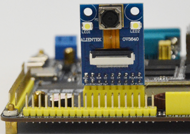
Figure 7.5.13.1 hardware connection diagram of development board
Next, we turn on the power switch and download the program. After the program is downloaded, there is no phenomenon on the development board. Next, we open the upper computer of punctual atomic UDP transmission video display, which is located on the data disk (disk A) / 6_ Software data / 1_ Software / video_ Under the transfer folder, as shown in the following figure:

Figure 7.5.13.2 opening the upper computer software
Double click video_transfer.exe to open the software. If the software cannot be opened, double-click to install VC in the figure above_ redist. x64. Exe, and then open video after installation_ transfer. exe.
The opened interface is shown in the following figure.
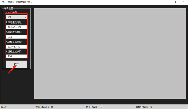
Figure 7.5.13.3 upper computer setting interface
Set according to the interface above. These settings correspond to the parameters and codes defined in the program. After setting, click the "open" button. At this time, the upper opportunity sends ASCII code "1" to the development board through the network port. After receiving the start command, the development board will start transmitting image data, as shown in the following figure:
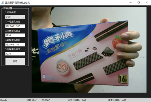
Figure 7.5.13.4 real time display screen of upper computer
It can be seen from the above figure that the image resolution transmitted by the development board is 640 * 480 and the frame rate is about 26fps. If you need to stop the display, just click the "close" button above. It should be noted that the screen displayed by the upper computer is affected by the computer performance. If the computer performance is poor, the upper computer may get stuck and crash.