Introduction to MIG IP core
In Xilinx series FPGA, in order to facilitate users to read and write DDR, the official provides an IP core MIG for accessing DDR, which is fully called Memory Interface Generator. For details, please refer to the official Xilinx document reference manual: ug586(7 Series Devices Memory Interface Solutions v4.1). The following figure shows the architecture of MIG IP core. It can be seen from the figure that MIG mainly has user oriented ports and DDR oriented ports. Users can access DDR SDRAM through the signals of user ports by using MIG, so as to simplify operation.
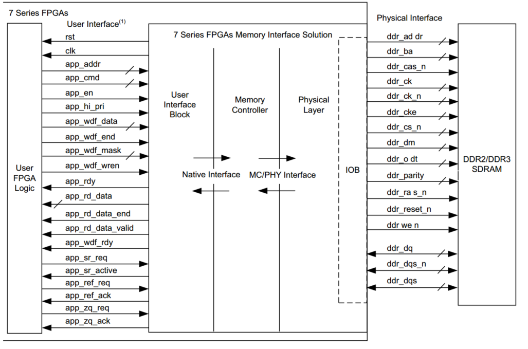
In this article, we only focus on some user oriented ports, namely the following ports:
clk,rst
app_addr,app_cmd,app_en,app_rdy
app_wdf_wren,app_wdf_end,app_wdf_rdy,app_wdf_data
app_rd_data,app_rd_data_valid
Among them, the first line signal is the global clock and reset signal, the second line signal is the command channel signal for issuing the read-write command, the third line signal is the write data channel signal, and the last line signal is the read data channel signal.
Command channel
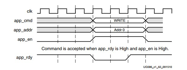
As shown in the figure above, app_cmd is used to specify the command. 3'b000 is a write command, and 3'b001 is a read command. app_addr is the corresponding read / write address, and the command will only be displayed in app_en and app_ When RDY is both high, it will be accepted.
Read data channel
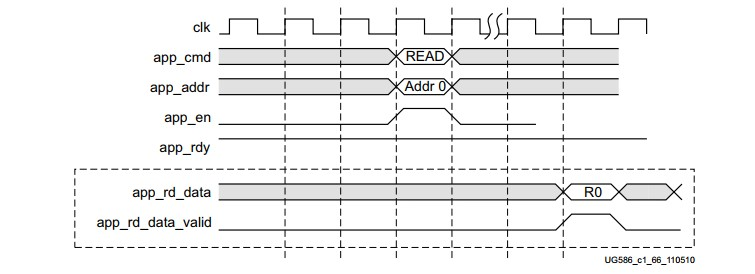
As shown in the figure above, the timing of reading data is relatively simple. After the read command is issued, after several clock cycles, app_rd_data_ The valid signal will be pulled up, and the corresponding app_rd_data is the read data.
Write data channel
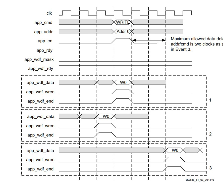
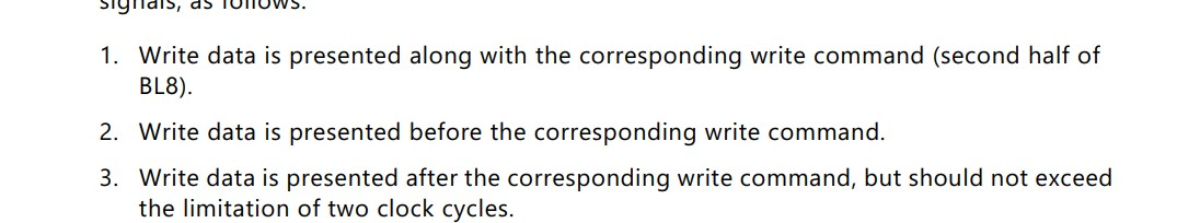
The above figure is a write sequence diagram of MIG controller and the official explanation of these write operations. Through the introduction of official documents, we can know that the written data can be given before, at or after the write command, but the written data given after the write command cannot exceed two clock cycles. There are no such restrictions if write data is given before the write command. The reason for this operation is that there is a FIFO to write data in the IP core, which can buffer the data.
In this paper, we use 1 this way of data writing.
DDR3 MIG experiment
In this experiment, we implemented an interface conversion: the app on the user side of MIG_* The interface signal is converted into AXI4 interface signal for users to call more conveniently.
The converted code is as follows:
`timescale 1ns / 1ps
//
// Company:
// Engineer:
//
// Create Date: 2022/01/03 10:38:32
// Design Name:
// Module Name: mig2axi4
// Project Name:
// Target Devices:
// Tool Versions:
// Description:
//
// Dependencies:
//
// Revision:
// Revision 0.01 - File Created
// Additional Comments:
//
//


module mig2axi4(
//AXI4 interface
//Global signal
input logic ACLK,
input logic ARESETn,
//Read address channel
input logic [31:0] ARADDR,
input logic [7:0] ARLEN,
input logic [2:0] ARSIZE,               //2^7=128
input logic [1:0] ARBURST,
input logic [2:0] ARPROT,
input logic ARVALID,
output logic ARREADY,
//Read data channel
output logic RVALID,
output logic [127:0] RDATA,
output logic [1:0] RRESP,
output logic RLAST,
input logic RREADY,
//Write address channel
input logic [31:0] AWADDR,
input logic [7:0] AWLEN,
input logic [2:0] AWSIZE,
input logic [1:0] AWBURST,
input logic [2:0] AWPROT,
input logic AWVALID,
output logic AWREADY,
//Write data channel
input logic [127:0]WDATA,
input logic [15:0] WSTRB,
input logic WLAST,
input logic WVALID,
output logic WREADY,
//Write reply channel
output logic [1:0] BRESP,
output logic BVALID,
input logic BREADY,
//MIG side interface
input  logic ui_clk,
input  logic ui_clk_sync_rst,
input  logic init_calib_complete,
input  logic app_rdy,
input  logic app_wdf_rdy,
input  logic app_rd_data_valid,
input  logic [127:0]   app_rd_data,
output logic [27:0]    app_addr,
output logic app_en,
output logic app_wdf_wren,
output logic app_wdf_end,
output logic [2:0]     app_cmd,               //3'b000 is write data and 3'b001 is read data
output logic [127:0]   app_wdf_data
    );

logic [31:0] rd_base_addr;                       //Address increment 128 / 16 = 8 each time
logic [8:0]  rd_len;
logic [31:0] wr_base_addr;
logic [8:0] wr_len;
logic [127:0] rd_buffer [0:255];                  //Read data cache
logic [31:0] rd_cnt;                              //Number of data in data cache
logic [31:0] rd_cmd_cnt;                          //Number of read commands
logic [31:0] wr_cnt;
logic [31:0] send_cnt;                            //Number of data sent
typedef enum bit [7:0] {
    IDLE,
    READ,
    WRITE
} State;
State cur_state,next_state;
//cur_state
always_ff@(posedge ACLK,negedge ARESETn)
if(!ARESETn)
    cur_state<=IDLE;
else
    cur_state<=next_state;
//next_state
always_comb
begin
    case(cur_state)
        IDLE:if(ARVALID)
                 next_state=READ;
             else if(AWVALID)
                 next_state=WRITE;
             else
                 next_state=IDLE;
        WRITE:if(BVALID&&BREADY&&BRESP==2'b00)
                  next_state=IDLE;
              else
                  next_state=WRITE;
        READ:if(RVALID&&RREADY&&RLAST)          //The last data read is complete
                 next_state=IDLE;
             else
                 next_state=READ;
        default:next_state=IDLE;
    endcase
end
/********************************************************Read data***************************************************/
//ARREADY
always_ff@(posedge ACLK,negedge ARESETn)
if(~ARESETn)
    ARREADY<=0;
else if(ARVALID&&~ARREADY)
    ARREADY<=1;
else if(ARREADY&&ARVALID)                       //Read address channel handshake completed
    ARREADY<=0;
//rd_base_addr
always_ff@(posedge ACLK,negedge ARESETn)
if(~ARESETn)
    rd_base_addr<=0;
else if(ARVALID&&ARREADY)
    rd_base_addr<=ARADDR;
//rd_len
always_ff@(posedge ACLK,negedge ARESETn)
if(~ARESETn)
    rd_len<=0;
else if(ARVALID&&ARREADY)
    rd_len<=ARLEN+1;
//app_cmd
always_comb
if(cur_state==WRITE)
    app_cmd=3'b000;
else if(cur_state==READ)
    app_cmd=3'b001;
else
    app_cmd=3'b000;
//app_en
always_comb
case(cur_state)
     IDLE:app_en=0;
     READ:if(rd_cmd_cnt<rd_len&&app_rdy)                 //app_rdy is high and the number of read commands has not reached rd_len
              app_en=1;
          else
              app_en=0;
     WRITE:if(app_rdy&&app_wdf_rdy&&WVALID)               //When DDR is ready to accept data and WDATA is valid, pull up the app_en
              app_en=1;
           else
              app_en=0;
     default:app_en=0;
endcase
//app_addr
always_ff@(posedge ACLK)
if(ARVALID&&ARREADY)
    app_addr<=ARADDR;
else if(AWVALID&&AWREADY)
    app_addr<=AWADDR;
else if(app_en&&app_rdy)                               //Write data successfully or send read command successfully
    app_addr<=app_addr+8;
//rd_cmd_cnt
always_ff@(posedge ACLK,negedge ARESETn)
if(~ARESETn)
    rd_cmd_cnt<=0;
else if(cur_state==READ&&app_en&&app_rdy)      //Issue a read command
    rd_cmd_cnt<=rd_cmd_cnt+1;
else if(cur_state==IDLE)
    rd_cmd_cnt<=0;
//rd_cnt
always_ff@(posedge ACLK,negedge ARESETn)
if(~ARESETn)
    rd_cnt<=0;
else if(app_rd_data_valid)
    rd_cnt<=rd_cnt+1;
else if(cur_state==IDLE)
    rd_cnt<=0;
//rd_buffer
always_ff@(posedge ACLK)
if(app_rd_data_valid)
    rd_buffer[rd_cnt]<=app_rd_data;                                                //Data cache
//send_cnt
always_ff@(posedge ACLK,negedge ARESETn)
if(~ARESETn)
    send_cnt<=0;
else if(ARVALID&&ARREADY)
    send_cnt<=0;
else if(rd_cnt==rd_len&&RVALID&&RREADY)                                         //Data cache completed
    send_cnt<=send_cnt+1;
else if(cur_state==IDLE)
    send_cnt<=0;
//RVALID
always_ff@(posedge ACLK,negedge ARESETn)
if(~ARESETn)
    RVALID<=0;
else if(rd_cnt==rd_len&&RVALID&&RREADY&&RLAST)                    //After send_cnt==rd_len
    RVALID<=0;
else if(rd_cnt==rd_len&&send_cnt<rd_len)
    RVALID<=1;
//RDATA
always_comb
    RDATA=rd_buffer[send_cnt];
//RLAST
always_ff@(posedge ACLK,negedge ARESETn)
if(~ARESETn)
    RLAST<=0;
else if(send_cnt==rd_len-2&&RVALID&&RREADY)                        //After the penultimate data is sent, pull up RLAST, indicating that the next data is the last data
    RLAST<=1;
else if(send_cnt==rd_len-1&&RVALID&&RREADY&&RLAST)                 //When the last data transmission is completed, pull down RLAST
    RLAST<=0;
/***************************************************************************Write data*******************************************************************/
//awready
always_ff @(posedge ACLK)
begin
    if(~ARESETn)
        AWREADY<=0;
    else if(AWVALID&&~AWREADY)
        AWREADY<=1;
    else if(AWVALID&&AWREADY)                //Write address channel handshake completed
        AWREADY<=0;
end
//wr_len
always_ff@(posedge ACLK)
if(AWVALID&&AWREADY)
    wr_len<=AWLEN+1;
//wr_base_addr
always_ff@(posedge ACLK)
if(AWVALID&&AWREADY)
    wr_base_addr<=AWADDR;
//app_wdf_wren if app_ RDY and app_ wdf_ If RDY and WVALID are both high, pull up app_wdf_wren and wready (WVALID is high description data valid, app_rdy and app_wdf_rdy are high description DDR writable data)
always_comb
if(cur_state==WRITE&&app_rdy&&app_wdf_rdy&&WVALID)
     app_wdf_wren=1;
else
     app_wdf_wren=0;
//wready
assign WREADY=app_wdf_wren;
//app_wdf_end
assign app_wdf_end=app_wdf_wren;
//app_wdf_data
assign app_wdf_data=WDATA;
//BRESP
assign BRESP=2'b00;         //OK
//BVALID
always_ff@(posedge ACLK,negedge ARESETn)
if(~ARESETn)
    BVALID<=0;
else if(WVALID&&WREADY&&WLAST)            //After the last data is written, pull up the BVALID
    BVALID<=1;
else if(BVALID&&BREADY&&BRESP==2'b00)     //Write response channel handshake completed
    BVALID<=0;
//BID
endmodule
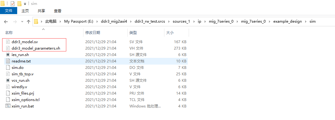
We use the DDR3 simulation model provided by MIG IP to simulate, as shown in the figure below, just add ddr3_model.sv and ddr3_model_parameters.vh file to the simulation platform.
The following code is used to generate AXI4 test signal:
axi4_master.sv
`timescale 1ns / 1ps
//
// Company:
// Engineer:
//
// Create Date: 2022/01/03 12:56:25
// Design Name:
// Module Name: axi4_master
// Project Name:
// Target Devices:
// Tool Versions:
// Description:
//
// Dependencies:
//
// Revision:
// Revision 0.01 - File Created
// Additional Comments:
//
//


module axi4_master(
input logic ACLK,
input logic ARESETn,
//Read address channel
output logic [31:0] ARADDR,
output logic [7:0] ARLEN,
output logic ARVALID,
input logic ARREADY,
//Read data channel
input logic [127:0] RDATA,
input logic [1:0] RRESP,
input logic RLAST,
input logic RVALID,
output logic RREADY,
//Write address channel
output logic [31:0] AWADDR,
output logic [7:0] AWLEN,
output logic AWVALID,
input logic AWREADY,
//Write data channel
output logic [127:0] WDATA,
output logic [15:0] WSTRB,
output logic WLAST,
output logic WVALID,
input logic WREADY,
//Write reply channel
input logic [1:0] BRESP,
input logic BVALID,
output logic BREADY,
//Initialization completion signal
input  logic init_calib_complete
    );
parameter WRITE_BASE_ADDR = 256;
parameter READ_BASE_ADDR = 256;
parameter TEST_LEN = 32-1;
logic init_calib_complete_d1;
logic start;
logic [31:0] wr_cnt;
logic [31:0] rd_cnt;
//start
assign start=init_calib_complete&(~init_calib_complete_d1);
//init_calib_complete_d1
always_ff@(posedge ACLK)
    init_calib_complete_d1<=init_calib_complete;
//Write 16 data
//AWADDR
assign AWADDR=WRITE_BASE_ADDR;
//AWLEN
assign AWLEN=TEST_LEN;
//AWVALID
always_ff@(posedge ACLK,negedge ARESETn)
if(~ARESETn)
    AWVALID<=0;
else if(start)
    AWVALID<=1;
else if(AWVALID&&AWREADY)
    AWVALID<=0;
//WDATA
always_comb
    WDATA=wr_cnt;
//WSTRB
assign WSTRB=16'hffff;
//WLAST
always_ff@(posedge ACLK,negedge ARESETn)
if(~ARESETn)
    WLAST<=0;
else if(WVALID&&WREADY&&wr_cnt==TEST_LEN+1-2)            //Penultimate data write completed
    WLAST<=1;
else if(WVALID&&WREADY&&WLAST)                         //The last data transmission is completed
    WLAST<=0;
//WVALID
always_ff@(posedge ACLK,negedge ARESETn)
if(~ARESETn)
   WVALID<=0;
else if(AWVALID&&AWREADY)
   WVALID<=1;
else if(WVALID&&WREADY&&WLAST)
   WVALID<=0;
//BREADY
always_ff@(posedge ACLK,negedge ARESETn)
if(~ARESETn)
    BREADY<=0;
else if(AWVALID&&AWREADY)
    BREADY<=1;
else if(BVALID&&BREADY&&BRESP==2'b00)
    BREADY<=0;
//wr_cnt
always_ff@(posedge ACLK,negedge ARESETn)
if(~ARESETn)
    wr_cnt<=0;
else if(start)
    wr_cnt<=0;
else if(WVALID&&WREADY)
    wr_cnt<=wr_cnt+1;
//Read 16 data
//ARADDR
assign ARADDR=READ_BASE_ADDR;
//ARLEN
assign  ARLEN=TEST_LEN;
//ARVALID
always_ff@(posedge ACLK,negedge ARESETn)
if(~ARESETn)
    ARVALID<=0;
else if(BVALID&&BREADY)
    ARVALID<=1;
else if(ARVALID&&ARREADY)
    ARVALID<=0;
//rready
always_ff@(posedge ACLK,negedge ARESETn)
if(~ARESETn)
    RREADY<=0;
else if(ARVALID&&ARREADY)
    RREADY<=1;
else if(RVALID&&RREADY&&RLAST)
    RREADY<=0;

endmodule
The top-level file of the whole project is top SV is:
`timescale 1ns / 1ps
//
// Company:
// Engineer:
//
// Create Date: 2022/01/03 14:22:32
// Design Name:
// Module Name: top
// Project Name:
// Target Devices:
// Tool Versions:
// Description:
//
// Dependencies:
//
// Revision:
// Revision 0.01 - File Created
// Additional Comments:
//
//


module top(
input              sys_clk,         //ϵͳʱ��
input              sys_rst_n,       //��λ,����Ч
// DDR3
inout [15:0]       ddr3_dq,         //DDR3 ����
inout [1:0]        ddr3_dqs_n,      //DDR3 dqs��
inout [1:0]        ddr3_dqs_p,      //DDR3 dqs��
output [13:0]      ddr3_addr,       //DDR3 ��ַ
output [2:0]       ddr3_ba,         //DDR3 banck ѡ��
output             ddr3_ras_n,      //DDR3 ��ѡ��
output             ddr3_cas_n,      //DDR3 ��ѡ��
output             ddr3_we_n,       //DDR3 ��дѡ��
output             ddr3_reset_n,    //DDR3 ��λ
output [0:0]       ddr3_ck_p,       //DDR3 ʱ����
output [0:0]       ddr3_ck_n,       //DDR3 ʱ�Ӹ�
output [0:0]       ddr3_cke,        //DDR3 ʱ��ʹ��
output [0:0]       ddr3_cs_n,       //DDR3 Ƭѡ
output [1:0]       ddr3_dm,         //DDR3_dm
output [0:0]       ddr3_odt         //DDR3_odt
    );

//axi interface
logic ACLK;
logic ARESETn;
//Read address channel
logic [31:0] ARADDR;
logic [7:0] ARLEN;
logic ARVALID;
logic ARREADY;
//Read data channel
logic [127:0] RDATA;
logic [1:0] RRESP;
logic RLAST;
logic RVALID;
logic RREADY;
//Write address channel
logic [31:0] AWADDR;
logic [7:0] AWLEN;
logic AWVALID;
logic AWREADY;
//Write data channel
logic [127:0] WDATA;
logic [15:0] WSTRB;
logic WLAST;
logic WVALID;
logic WREADY;
//Write reply channel
logic [1:0] BRESP;
logic BVALID;
logic BREADY;
//mig interface
logic app_rdy;
logic app_wdf_rdy;
logic app_rd_data_valid;
logic [127:0] app_rd_data;
logic [27:0] app_addr;
logic app_en;
logic app_wdf_wren;
logic app_wdf_end;
logic [2:0] app_cmd;               //3'b000 is write data and 3'b001 is read data
logic [127:0] app_wdf_data;
logic init_calib_complete;
//
logic clk_200;
logic ui_clk;
logic ui_clk_sync_rst;
logic locked;
//
assign ACLK=ui_clk;
assign ARESETn=~ui_clk_sync_rst;
//ddr side signal
// logic ddr3_addr                      (ddr3_addr),   // output [14:0]	ddr3_addr
// logic ddr3_ba                        (ddr3_ba),     // output [2:0]	ddr3_ba
// logic ddr3_cas_n                     (ddr3_cas_n),  // output		ddr3_cas_n
// logic ddr3_ck_n                      (ddr3_ck_n),   // output [0:0]	ddr3_ck_n
// logic ddr3_ck_p                      (ddr3_ck_p),   // output [0:0]	ddr3_ck_p
// logic ddr3_cke                       (ddr3_cke),    // output [0:0]	ddr3_cke
// logic ddr3_ras_n                     (ddr3_ras_n),  // output		ddr3_ras_n
// logic ddr3_reset_n                   (ddr3_reset_n),// output		ddr3_reset_n
// logic ddr3_we_n                      (ddr3_we_n),   // output		ddr3_we_n
// logic ddr3_dq                        (ddr3_dq),     // inout [31:0]	ddr3_dq
// logic ddr3_dqs_n                     (ddr3_dqs_n),  // inout [3:0]	ddr3_dqs_n
// logic ddr3_dqs_p                     (ddr3_dqs_p),  // inout [3:0]	ddr3_dqs_p
// logic ddr3_cs_n                      (ddr3_cs_n),   // output [0:0]	ddr3_cs_n
// logic ddr3_dm                        (ddr3_dm),     // output [3:0]	ddr3_dm
// logic ddr3_odt                       (ddr3_odt),    // output [0:0]	ddr3_odt

//Modular instantiation
axi4_master U1(
.ACLK(ACLK),
.ARESETn(ARESETn),
//Read address channel
.ARADDR(ARADDR),
.ARLEN(ARLEN),
.ARVALID(ARVALID),
.ARREADY(ARREADY),
//Read data channel
.RVALID(RVALID),
.RDATA(RDATA),
.RRESP(RRESP),
.RLAST(RLAST),
.RREADY(RREADY),
//Write address channel
.AWADDR(AWADDR),
.AWLEN(AWLEN),
.AWVALID(AWVALID),
.AWREADY(AWREADY),
//Write data channel
.WDATA(WDATA),
.WSTRB(WSTRB),
.WLAST(WLAST),
.WVALID(WVALID),
.WREADY(WREADY),
//Write reply channel
.BRESP(BRESP),
.BVALID(BVALID),
.BREADY(BREADY),
//Initialization completion signal
.init_calib_complete(init_calib_complete)
    );


mig2axi4 U2(
//AXI4 interface
//Global signal
.ACLK(ACLK),
.ARESETn(ARESETn),
//Read address channel
.ARADDR(ARADDR),
.ARLEN(ARLEN),
.ARSIZE(),               //2^7=128
.ARBURST(),
.ARPROT(),
.ARVALID(ARVALID),
.ARREADY(ARREADY),
//Read data channel
.RVALID(RVALID),
.RDATA(RDATA),
.RRESP(RRESP),
.RLAST(RLAST),
.RREADY(RREADY),
//Write address channel
.AWADDR(AWADDR),
.AWLEN(AWLEN),
.AWSIZE(),
.AWBURST(),
.AWPROT(),
.AWVALID(AWVALID),
.AWREADY(AWREADY),
//Write data channel
.WDATA(WDATA),
.WSTRB(WSTRB),
.WLAST(WLAST),
.WVALID(WVALID),
.WREADY(WREADY),
//Write reply channel
.BRESP(BRESP),
.BVALID(BVALID),
.BREADY(BREADY),
//MIG side interface
.ui_clk(ui_clk),
.ui_clk_sync_rst(ui_clk_sync_rst),
.init_calib_complete(init_calib_complete),
.app_rdy(app_rdy),
.app_wdf_rdy(app_wdf_rdy),
.app_rd_data_valid(app_rd_data_valid),
.app_rd_data(app_rd_data),
.app_addr(app_addr),
.app_en(app_en),
.app_wdf_wren(app_wdf_wren),
.app_wdf_end(app_wdf_end),
.app_cmd(app_cmd),               //3'b000 is write data and 3'b001 is read data
.app_wdf_data(app_wdf_data)
    );

mig_7series_0 u_mig_7series_0 (
    // Memory interface ports
    .ddr3_addr                      (ddr3_addr),   // output [14:0]	ddr3_addr
    .ddr3_ba                        (ddr3_ba),     // output [2:0]	ddr3_ba
    .ddr3_cas_n                     (ddr3_cas_n),  // output		ddr3_cas_n
    .ddr3_ck_n                      (ddr3_ck_n),   // output [0:0]	ddr3_ck_n
    .ddr3_ck_p                      (ddr3_ck_p),   // output [0:0]	ddr3_ck_p
    .ddr3_cke                       (ddr3_cke),    // output [0:0]	ddr3_cke
    .ddr3_ras_n                     (ddr3_ras_n),  // output		ddr3_ras_n
    .ddr3_reset_n                   (ddr3_reset_n),// output		ddr3_reset_n
    .ddr3_we_n                      (ddr3_we_n),   // output		ddr3_we_n
    .ddr3_dq                        (ddr3_dq),     // inout [31:0]	ddr3_dq
    .ddr3_dqs_n                     (ddr3_dqs_n),  // inout [3:0]	ddr3_dqs_n
    .ddr3_dqs_p                     (ddr3_dqs_p),  // inout [3:0]	ddr3_dqs_p
    .init_calib_complete            (init_calib_complete),
                                                   // init_calib_complete
	.ddr3_cs_n                      (ddr3_cs_n),   // output [0:0]	ddr3_cs_n
    .ddr3_dm                        (ddr3_dm),     // output [3:0]	ddr3_dm
    .ddr3_odt                       (ddr3_odt),    // output [0:0]	ddr3_odt
    // Application interface ports
    .app_addr                       (app_addr),    // input [28:0]	app_addr
    .app_cmd                        (app_cmd),     // input [2:0]	app_cmd
    .app_en                         (app_en),      // input			app_en
    .app_wdf_data                   (app_wdf_data),// input [255:0] app_wdf_data
    .app_wdf_end                    (app_wdf_end), // input         app_wdf_end
    .app_wdf_wren                   (app_wdf_wren),// input	        app_wdf_wren
    .app_rd_data                    (app_rd_data), // output [255:0]app_rd_data
    .app_rd_data_end                (app_rd_data_end),
                                                   // output	    app_rd_data_end
    .app_rd_data_valid              (app_rd_data_valid),
                                                   // output	    app_rd_data_valid
    .app_rdy                        (app_rdy),     // output	    app_rdy
    .app_wdf_rdy                    (app_wdf_rdy), // output	    app_wdf_rdy
    .app_sr_req                     (1'b0),            // input	        app_sr_req
    .app_ref_req                    (1'b0),            // input	        app_ref_req
    .app_zq_req                     (1'b0),            // input	        app_zq_req
    .app_sr_active                  (app_sr_active),// output	    app_sr_active
    .app_ref_ack                    (app_ref_ack),  // output	    app_ref_ack
    .app_zq_ack                     (app_zq_ack),   // output	    app_zq_ack
    .ui_clk                         (ui_clk),       // output	    ui_clk
    .ui_clk_sync_rst                (ui_clk_sync_rst),
                                                    // output       ui_clk_sync_rst
    .app_wdf_mask                   (31'b0),        // input [31:0]	app_wdf_mask
    // System Clock Ports
    .sys_clk_i                      (clk_200),
    // Reference Clock Ports
    .clk_ref_i                      (clk_200),
    .sys_rst                        (sys_rst_n)     // input         sys_rst
    );

//PLLģ��
clk_wiz_0 u_clk_wiz_0
   (
    // Clock out ports
    .clk_out1(clk_200),     // output clk_out1
    // Status and control signals
    .reset(1'b0),           // input resetn
    .locked(locked),        // output locked
   // Clock in ports
    .clk_in1(sys_clk)
    );

endmodule
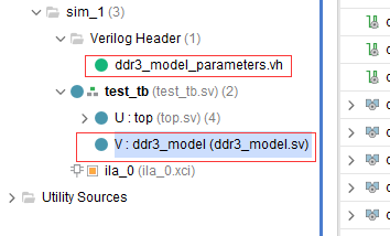
The test platform files are written as follows. Only the top module and ddr3 simulation model module can be instantiated:
test_tb.sv
`timescale 1ns / 1ps
//
// Company:
// Engineer:
//
// Create Date: 2021/12/29 20:23:18
// Design Name:
// Module Name: test_tb
// Project Name:
// Target Devices:
// Tool Versions:
// Description:
//
// Dependencies:
//
// Revision:
// Revision 0.01 - File Created
// Additional Comments:
//
//


module test_tb(

    );
parameter T=20;
    //
logic led;
logic sys_clk;
logic sys_rst_n;
//
wire   [13:0]		ddr3_addr;

wire   [2:0]		ddr3_ba;

wire  			ddr3_cas_n;

wire   [0:0]		ddr3_ck_n;

wire   [0:0]		ddr3_ck_p;

wire   [0:0]		ddr3_cke;

wire  			ddr3_ras_n;

wire  			ddr3_reset_n;

wire  			ddr3_we_n;

wire  [15:0]		ddr3_dq;

wire  [1:0]		ddr3_dqs_n;

wire  [1:0]		ddr3_dqs_p;

wire   [0:0]		ddr3_cs_n;

wire   [1:0]		ddr3_dm;

wire   [0:0]		ddr3_odt;
//sys_clk
initial begin
    sys_clk=0;
    forever begin
        #(T/2) sys_clk=~sys_clk;
    end
end
//sys_rst_n
initial begin
   sys_rst_n=0;
   #(10*T)
   sys_rst_n=1;
end

//
// ddr3_rw_top U(
//    .sys_clk(sys_clk),         //
//    .sys_rst_n(sys_rst_n),       //
//     // DDR3
//    .ddr3_dq(ddr3_dq),         //
//    .ddr3_dqs_n(ddr3_dqs_n),      //
//    .ddr3_dqs_p(ddr3_dqs_p),      //
//    .ddr3_addr(ddr3_addr),       //
//    .ddr3_ba(ddr3_ba),         //
//    .ddr3_ras_n(ddr3_ras_n),      //
//    .ddr3_cas_n(ddr3_cas_n),      //
//    .ddr3_we_n(ddr3_we_n),       //
//    .ddr3_reset_n(ddr3_reset_n),    //
//    .ddr3_ck_p(ddr3_ck_p),       //
//    .ddr3_ck_n(ddr3_ck_n),       //
//    .ddr3_cke(ddr3_cke),        //
//    .ddr3_cs_n(ddr3_cs_n),       //
//    .ddr3_dm(ddr3_dm),         //
//    .ddr3_odt(ddr3_odt),        //
//    .led(led)              //
//     );
top U(
.sys_clk(sys_clk),         //ϵͳʱ��
.sys_rst_n(sys_rst_n),       //��λ,����Ч
// DDR3
.ddr3_dq(ddr3_dq),         //DDR3 ����
.ddr3_dqs_n(ddr3_dqs_n),      //DDR3 dqs��
.ddr3_dqs_p(ddr3_dqs_p),      //DDR3 dqs��
.ddr3_addr(ddr3_addr),       //DDR3 ��ַ
.ddr3_ba(ddr3_ba),         //DDR3 banck ѡ��
.ddr3_ras_n(ddr3_ras_n),      //DDR3 ��ѡ��
.ddr3_cas_n(ddr3_cas_n),      //DDR3 ��ѡ��
.ddr3_we_n(ddr3_we_n),       //DDR3 ��дѡ��
.ddr3_reset_n(ddr3_reset_n),    //DDR3 ��λ
.ddr3_ck_p(ddr3_ck_p),       //DDR3 ʱ����
.ddr3_ck_n(ddr3_ck_n),       //DDR3 ʱ�Ӹ�
.ddr3_cke(ddr3_cke),        //DDR3 ʱ��ʹ��
.ddr3_cs_n(ddr3_cs_n),       //DDR3 Ƭѡ
.ddr3_dm(ddr3_dm),         //DDR3_dm
.ddr3_odt(ddr3_odt)         //DDR3_odt
);

ddr3_model V
(
    .rst_n   (ddr3_reset_n),
    .ck      (ddr3_ck_p),
    .ck_n    (ddr3_ck_n),
    .cke     (ddr3_cke),
    .cs_n    (ddr3_cs_n),
    .ras_n   (ddr3_ras_n),
    .cas_n   (ddr3_cas_n),
    .we_n    (ddr3_we_n),
    .dm_tdqs (ddr3_dm),
    .ba      (ddr3_ba),
    .addr    (ddr3_addr),
    .dq      (ddr3_dq),
    .dqs     (ddr3_dqs_p),
    .dqs_n   (ddr3_dqs_n),
    .tdqs_n  (),
    .odt     (ddr3_odt)
    );

endmodule
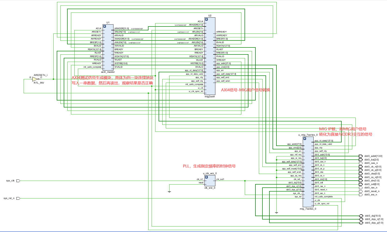
The following figure is the RTL view of the whole project, which well reveals the relationship between the above Codes:
Result analysis
AXI4 write data waveform
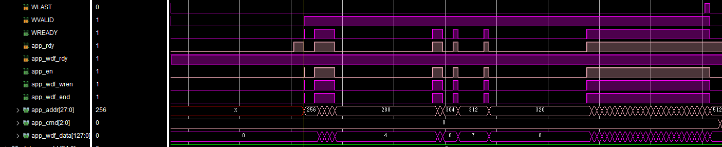
As you can see, when app_rdy,app_ wdf_ When RDY (indicating that ddr is ready to receive data) and WVALID signal (indicating that the data to be written is valid) are both high, app_en,app_wdf_wren and WREADY signals are pulled high and start writing a data.
AXI4 read data waveform
Write command

As shown in the figure, app_cmd is 3'b001, app_en,app_rdy is high, indicating that the read command has been accepted and app_addr is the address of the data to be read.
Read data
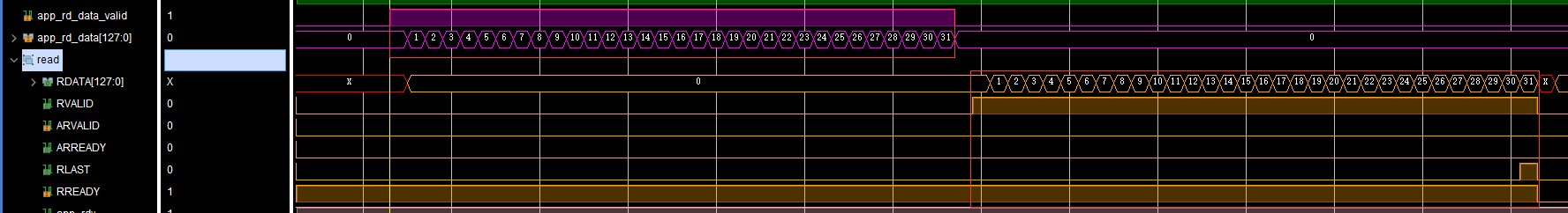
As shown in the figure, MIG stores the read data in the cache first, and then sends the data in the cache to the host through the read data channel of AXI4. (the efficiency of reading data can be further increased by using FIFO)