1 DDS principle
1.1 interpretation in the book
DDS (Direct Digital Synthesizer) technology is a new frequency synthesis method. It is a frequency synthesis technology that directly synthesizes the required waveform from the phase concept. It directly generates various signals of different frequencies and different waveforms by controlling the change speed of phase.
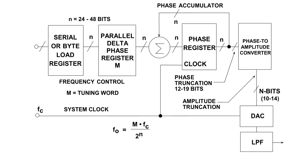
The core of the system is the phase accumulator, whose content will be updated every system clock. Each time the phase accumulator is updated, it is stored in Δ The digital word m in the phase register is accumulated to the number in the phase register. hypothesis Δ The number in the phase register is 00... 01 (i.e. M=1), and the initial content in the phase accumulator is 00... 00. The phase accumulator is updated by 00... 01 (M=1) every clock cycle. If the accumulator is 32 bits wide, 2 ^ 32 (more than 4 billion) clock cycles will be required before the phase accumulator returns to 00... 00, and the cycles will be repeated continuously.
The truncated output of the phase accumulator is used as the address of the sine (or cosine) lookup table. Each address in the lookup table corresponds to a sine
A phase point of the wave from 0 ° to 360 °. The lookup table includes the corresponding digital amplitude information for a complete sine wave period.
(in fact, only 90 ° data is required because the two MSB S contain orthogonal data). Therefore, the look-up table can change the phase
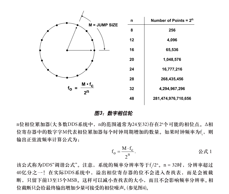
The phase information of the accumulator is mapped to the digital amplitude word to drive the DAC. Figure 3 shows this with a graphical "phase wheel"
This situation.
Consider the case of n = 32 and M = 1. The phase accumulator will step through each of the 2 ^ 32 (2^n/M) possible outputs until it overflows and starts again. The corresponding output sine wave frequency is equal to the input clock frequency 2 ^ 32. If M=2, the phase accumulator register will "scroll" at twice the speed and the output frequency will double. The above contents can be summarized as follows:
1.2 own understanding
DDS system is mainly composed of four major structures: phase accumulator, waveform memory, digital to analog (D/A) converter and low-pass filter. Its structural block diagram is shown in the figure below.
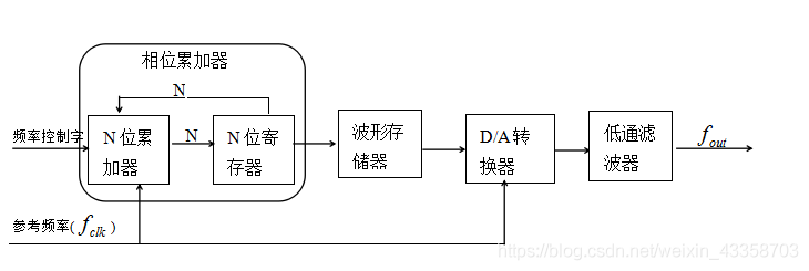
Reference clock:
In the figure, the reference frequency f_clk is a fixed value. Generally, we choose the system clock. Here, 100MHz is set.
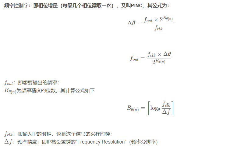
Frequency control word:
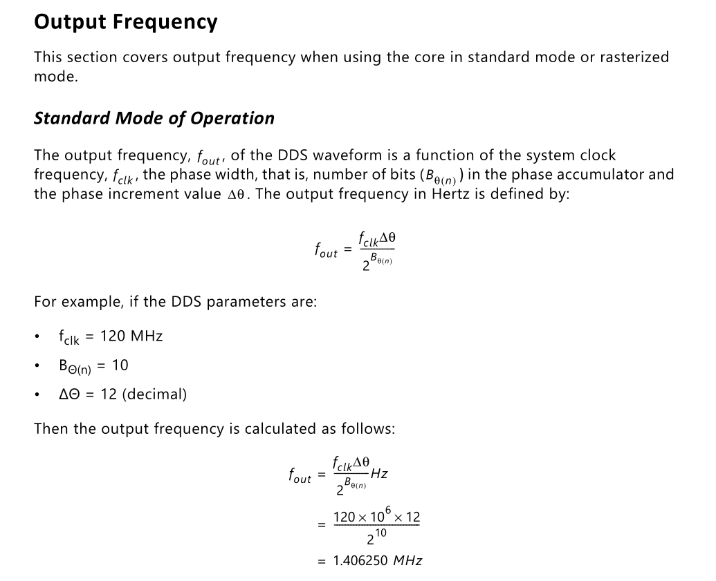
Used to adjust the frequency of the output signal. How to get the output frequency according to the reference frequency? The official document of DDS IP gives the corresponding formula.
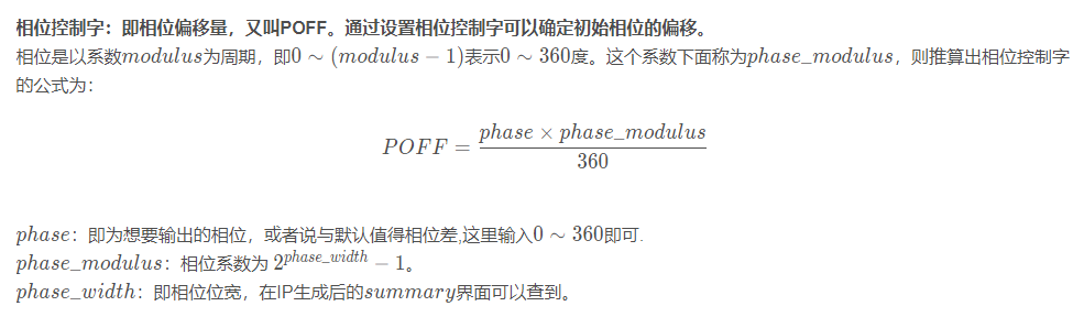
Phase control word:
Phase accumulator:
It is composed of N-bit adder and N-bit accumulation register. It completes the accumulation of phase value according to the frequency control word k, and inputs the accumulated value into the waveform memory.
Waveform memory:
Take the value of the phase accumulator as the current address, find the signal data corresponding to the phase value, and output it to the D/A converter.
D/A converter:
The digital quantity output by the waveform memory is converted into the corresponding analog quantity.
Low pass filter:
Due to the quantization error and aliasing in the output waveform of D/A converter, a low-pass filter needs to be used at the output to improve the output performance of the signal.
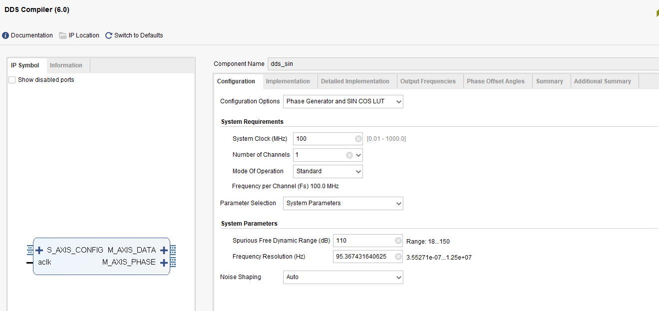
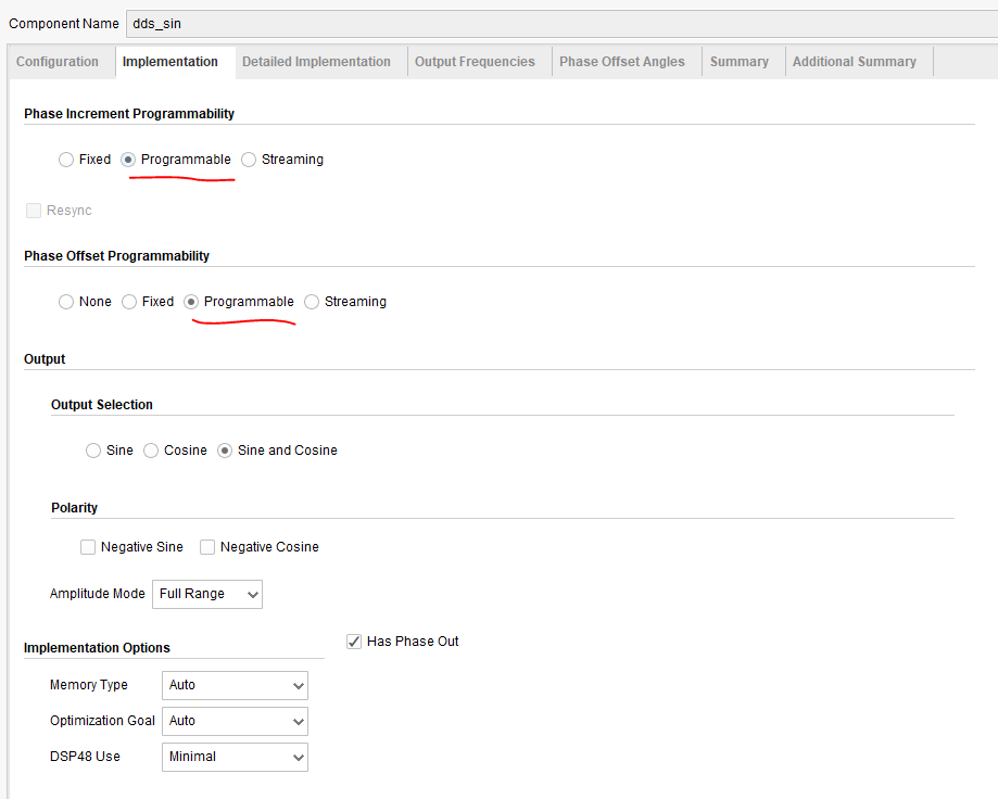
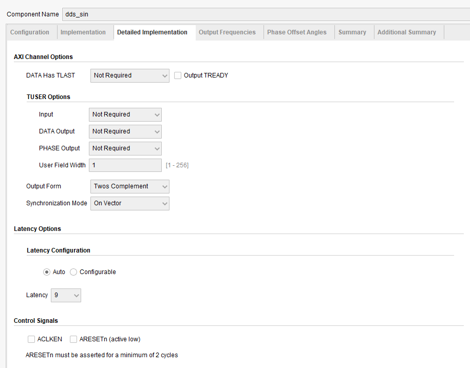
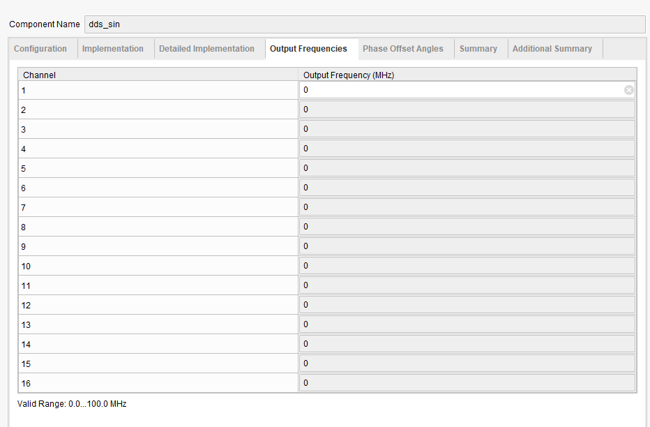
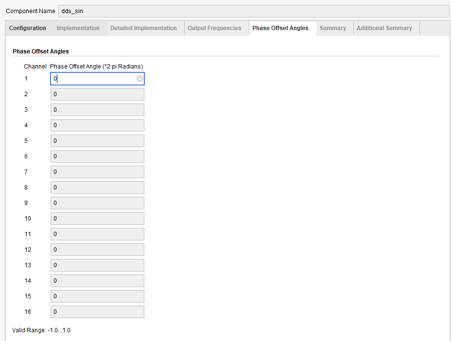
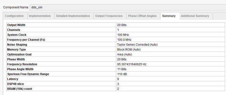
2. DDS IP parameter setting
3 source code
Program structure
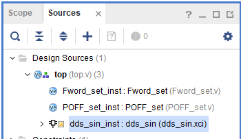
3.1 top level documents
`timescale 1ns / 1ps


module top(
    input           sys_clk         ,// System clock
    input           rst_n           ,// System reset
    input  [1:0]    key_PINC        ,// Key corresponding to frequency control word
    input  [1:0]    key_POFF         // Key corresponding to phase control word
    );


 //-----------Frequency control word module
wire  [23:0]   PINC ;  //Frequency word
Fword_set Fword_set_inst(
        //input
        .clk        (sys_clk            ),
        .rst_n      (rst_n              ),
        .key_PINC   (key_PINC           ),
        //output
        .PINC       (PINC               )
        );


 //-----------Phase control word module
 wire  [23:0]   POFF ;  //Phase word
POFF_set POFF_set_inst(
    //input
    .clk        (sys_clk   )    ,
    .rst_n      (rst_n     )    ,
    .key_POFF   (key_POFF  )    ,
    //output
    .POFF       (POFF      )
    );


 //-------------DDS module
//input
wire [0:0]   fre_ctrl_word_en  ;

//output
wire [0:0]   m_axis_data_tvalid    ;
wire [47:0]  m_axis_data_tdata     ;
wire [0:0]   m_axis_phase_tvalid   ;
wire [23:0]  m_axis_phase_tdata    ;

assign fre_ctrl_word_en=1'b1;

dds_sin dds_sin_inst (
  .aclk                 (sys_clk                ),    // input wire aclk
  .s_axis_config_tvalid (fre_ctrl_word_en       ),    // input wire s_axis_config_tvalid
  .s_axis_config_tdata  ({POFF,PINC}           ),    // input wire [47 : 0] s_axis_config_tdata

  .m_axis_data_tvalid   (m_axis_data_tvalid     ),    // output wire m_axis_data_tvalid
  .m_axis_data_tdata    (m_axis_data_tdata      ),    // output wire [47 : 0] m_axis_data_tdata
  .m_axis_phase_tvalid  (m_axis_phase_tvalid    ),    // output wire m_axis_phase_tvalid
  .m_axis_phase_tdata   (m_axis_phase_tdata     )     // output wire [23 : 0] m_axis_phase_tdata
);


endmodule
3.2 frequency control word module
`timescale 1ns / 1ps
//
// Press the key to select the corresponding frequency control word, and then select the corresponding signal frequency
//


module Fword_set(
    input               clk         ,
    input               rst_n       ,
    input  [1:0]        key_PINC    ,

    output reg [23:0]   PINC
    );


//always@(posedge clk or negedge rst_n)
//begin
//    if(!rst_n)
//        key_sel <= 4'd0;
//    else
//        key_sel <= key_sel;
//end


//  The output frequency(f_out ) , of the DDS waveform is a function of the system clock frequency(f_clk ) .
//  the phase width, that is, number of bits (B )  in the phase accumulator
//  and the phase increment value (deta_theta) .
//  The output frequency in Hertz is defined by:f_out=f_clk*deta_theta/(2^B)
//  fre_ ctrl_ How is word determined?
// According to the summery of the IP core, phase width = 20bits frequency per channel = 100MHz
// Calculation formula of output frequency f_out=f_clk*deta_theta/(2^B)=100M* 104857/(2^20 )= 10M
always@(*)
begin
    case(key_PINC)
        0:  PINC <= 'h28f5;     //1MHz 10485 value of each phase increase deta_theta
        1:  PINC <= 'h51eb;     //2Mhz  20971
        2:  PINC <= 'ha3d7;     //4Mhz  41943
        3:  PINC <= 'h19999;    //10Mhz  104857
    endcase
end


endmodule
3.3 phase control word module
`timescale 1ns / 1ps
//
// Press the key to select the corresponding phase control word, and then select the corresponding initial phase of the signal
/


module POFF_set(
    input               clk         ,
    input               rst_n       ,
    input  [1:0]        key_POFF    ,

    output [23:0]       POFF
    );


//always@(posedge clk or negedge rst_n)
//begin
//    if(!rst_n)
//        key_sel <= 4'd0;
//    else
//        key_sel <= key_sel;
//end


// According to the summery and phase of the IP core_ width=20bits   Frequency per channel=100MHz
// Calculation formula of output phase: POFF=phase*phase_modulus/360
// Phase: if you want to output the phase, enter 0 ~ 360
// phase_ Module: the phase coefficient is 2^phase_width-1=2^20-1,
// phase_width is the phase bit width, which can be viewed in the IP generation summary
reg  [8:0]   phase;    //0-360

always@(*)
begin
    case(key_POFF)
        0:  phase <= 'h0;         //0
        1:  phase <= 'h5a;        //90
        2:  phase <= 'hb4;        //180
        3:  phase <= 'h10e;       //270
    endcase
end

assign POFF=phase*1048575/360;


endmodule
3.4 testbench file
`timescale 1ns / 1ps


module sim_top;

    reg         sys_clk ;
    reg         rst_n   ;
    reg [1:0]   key_PINC;
    reg [1:0]   key_POFF;

    //Instantiate source file
    top top_inst(
       .sys_clk      (sys_clk      ),
       .rst_n        (rst_n        ),
       .key_PINC     (key_PINC     ),
       .key_POFF     (key_POFF     )
        );


    initial
        begin
            //initialization
            sys_clk=0;
            rst_n=0;
            key_PINC=2'd0;
            key_POFF=2'd0;  //30


            #100
            rst_n=1;
            key_PINC=0;  //1MHz 10485 value of each phase increase deta_theta
            #4000
            key_PINC=1;  //2Mhz  20971
            #4000
            key_PINC=2;  //4Mhz  41943
            #4000
            key_PINC=3;   //10Mhz  104857

            #4000
            key_POFF=1;  //60
            #4000
            key_POFF=2;  //90
            #4000
            key_POFF=3;   //180
        end


        // create clock;
        always #5 sys_clk=~sys_clk;// Every time the interval is 5ns, take one inverse, that is, the period is 10ns, so the frequency is 100MHz


endmodule
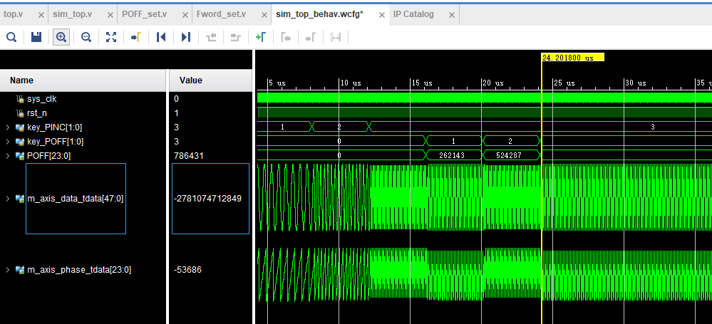
4 Results