1. Combination logic
Combinational logic refers to the logic circuit whose output is only related to the current input logic level and has nothing to do with the original state of the circuit. It belongs to memoryless circuit and is commonly used in multiplexers, adders, decoders, etc
1.1 implementation of assignment statement
The form of question mark expression
assign data_out = en ? a:b;
1.2 implementation of always block
The general application is mainly in the state transition judgment of the three segment state machine. The three segment state machine statements are: sub state transition to the present state, state transition condition judgment, sub state register output.
//Parameter declaration
parameter IDLE = 2'b00;
parameter S0 = 2'b01;
parameter S1 = 2'b10;

//Internal signal declaration
reg[1:0] current_state;
reg[1:0] next_state;

//signal output

reg data_out;

//The first section: saving the status register

always @ (posedge clk or negedge Rst_n)
begin
    if(!Rst_n)
        current_state <= IDLE;
    else
        current_state <= next_state;
end

//The combinational logic of the second segment of the secondary state
always @ (w_i or current_state)
begin
    case(current_state)
    IDLE: begin
            if(w_i) next_state = S0;
             else next_state = IDLE;
        end
    S0: begin
            if(w_i) next_state = S1;
            else next_state = IDLE;
        end
    S1: begin
            if(w_i) next_state = S1;
            else next_state = IDLE;
        end
    default : next_state = 2'bxx;
    endcase
end

//Section 3: output logic
always @ (*)
beign
    case(current)
        IDLE:   data_out = 1'b0;
        S0:     data_out = 1'b0;
        S1:     data_out = 1'b1;
        default: data_out = 1'b0;
    endcase
end
2. Sequential logic circuit
Sequential logic circuit contains memory elements (such as D flip-flop) which can store information temporarily and have memory. It is generally realized by always statement block. It can use posedge and nagedge to capture the rising or falling edge of clock to describe sequential logic circuit.
3. State machine
3.1 molar state machine
block diagram
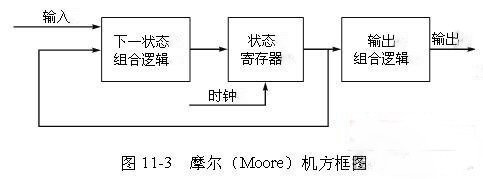
Code as section 1.2
3.2 milli state machine
[block diagram]
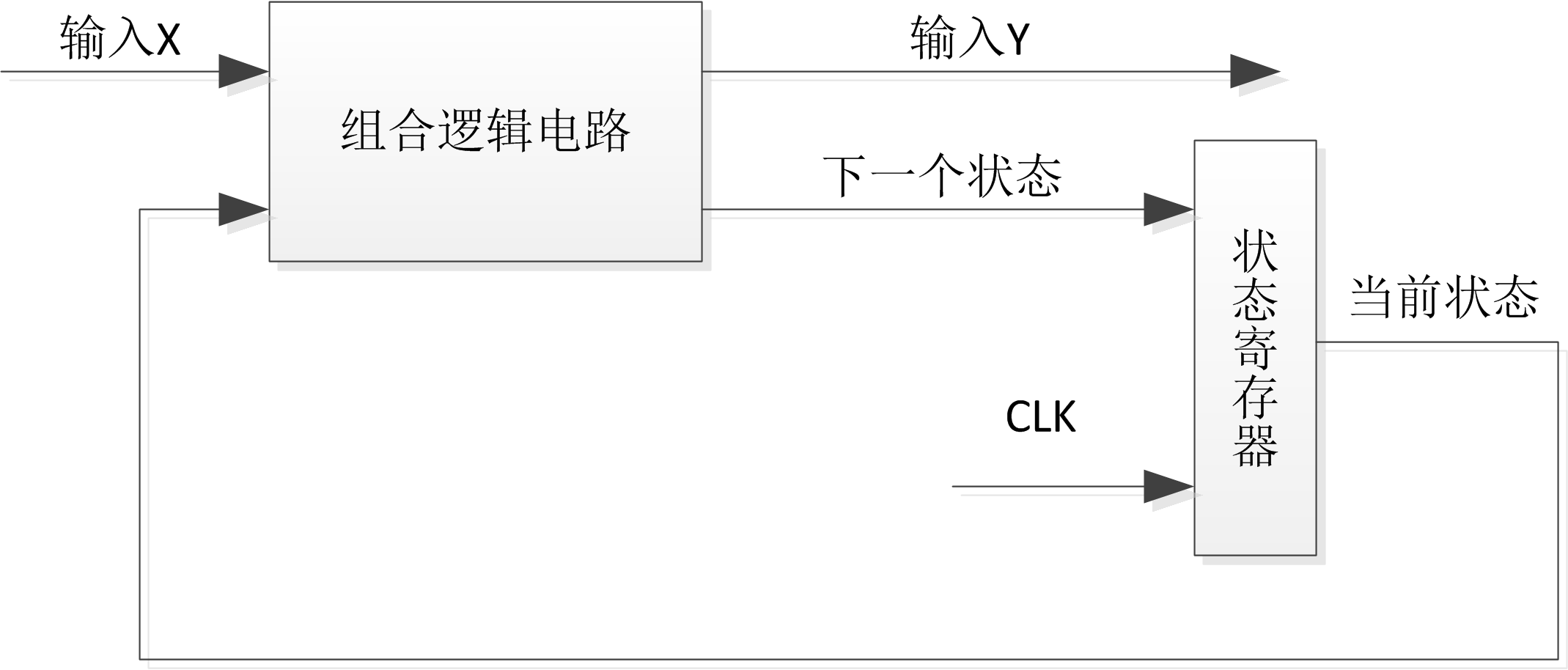
Code
//The first section: saving the status register

always @ (posedge clk )
begin
    current_state <= next_state;
end

//The second section combines logic and state output
always @ (w_i or current_state)
begin
    case(current_state)
    IDLE: begin
            data_out = 1'bz;
            if(w_i) next_state = S0;
             else next_state = IDLE;
        end
    S0: begin
            data_out = 1'b0;
            if(w_i) next_state = S1;
            else next_state = IDLE;
        end
    S1: begin
            data_out = 1'b1;
            if(w_i) next_state = S1;
            else next_state = IDLE;
        end
    default : next_state = 2'bxx;
    endcase
end
3. How to generate custom IP CORE in Quartus II software?
describe
You can use the Quartus ® II software to generate a custom IPCORE using the following steps:
1. Create a new project, add the customer verilog / VHDL code file, and set this file as the top-level entity. Then run Analysis & Elaboration.
2. Select the Quartus II software menu (Project - > export design partition...) And generate xxx.qxp file.
3. Use the generated xxx.qxp file as the IPCORE.