Topic 1. Differences between bit, byte, word, DWORD and qword
1byte = 8bit

1word = 2byte = 16bit

1dword = 2word = 4byte = 32bit

1qword = 2dword = 4word = 8byte = 64bit
Topic 2. What is the original code, inverse code, complement code, symbol value code. Taking 8bit as an example, the numerical ranges of their respective representations are given
Original code: symbol bit+True value, the highest bit represents the sign bit, expressed in 8 bit For example.
[+3]primary = 0000_0011
[-3]primary = 1000_0011
 Representation range:-127 reach+127
 0000 and 1000 in the original code represent 0.

Inverse code: the inverse code of a positive number is itself. The inverse code of a negative number reverses the original code bit by bit except for the sign bit. With 8 bit For example.
[+3]primary = [0000_0011]primary = [0000_0011]back
[-3]primary = [1000_0011]primary = [1111_1100]back
 Representation range:-127 reach+127
 0000 in inverse code_0000 And 1111_1111 All represent 0.

Complement: the complement of a positive number is itself. The complement of a negative number reverses the original code bit by bit except for the sign bit, and then adds 1. With 8 bit For example.
[+3]primary = [0000_0011]primary = [0000_0011]back = [0000_0011]repair
[-3]primary = [1000_0011]primary = [1111_1100]back = [1111_1101]repair
 Representation range:-128 reach+127

There is only one form of 0 in the complement, namely 0000_0000,1000_0000 express-128.
The above are signed numbers. For unsigned numbers, they all represent integers, and their original code, inverse code and complement are themselves.

For a more detailed explanation, please refer to Wikipedia.
https://zh.wikipedia.org/wiki/%E6%9C%89%E7%AC%A6%E8%99%9F%E6%95%B8%E8%99%95%E7
%90%86
Topic 3. Number system conversion
R Convert hexadecimal number to decimal number: expand by weight and add

Convert decimal numbers to R Hexadecimal number: integer part, divided by R The remainder method is divided until the quotient is 0. Decimal part, multiply by R Rounding method, multiply until the product is 0
 until.

Binary number into octal number: a group of three digits, with 0 on the left of integer part and 0 on the right of decimal part. vice versa.

Binary number into hexadecimal number: a group of four digits, with 0 on the left of integer part and 0 on the right of decimal part. vice versa.

127 -127 127.375 -127.375 Convert decimal numbers to R Hexadecimal number: integer part, divided by R The remainder method is divided until the quotient is 0. decimal
 Part, multiply R Rounding method, multiply until the product is 1.

127 = 0111_1111
-127 = 1111_1111
127.375 = 0111_1111.011
-127.375 = 1111_1111.011
Topic 4. Logic function and its simplification
Formula method
 Karnaugh map method
Topic 5. What are adventure and competition and how to eliminate them?
The following circuit uses two logic gates, a not gate and an and gate, which would have been ideal F The output of should be always stable
 But in fact, each gate circuit must have a time delay from input to output. This time is usually called the switch of the circuit
 Delay. Moreover, the manufacturing process, the type of door, and even the small process deviation during manufacturing will cause the change of the switching delay time.
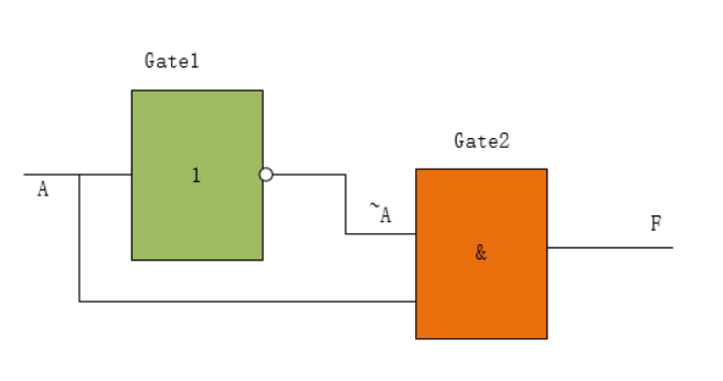
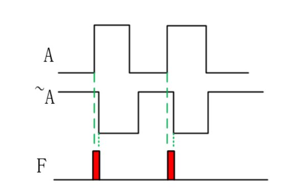
In fact, if you count the delay of the logic gate, then F Finally, burrs will occur. The phenomenon that the signal reaches a convergence point through different paths is called competition, and the phenomenon of instantaneous error in circuit output caused by competition is called adventure, FPGA The simplest way to avoid in the design is to use sequential logic to synchronize input and output as much as possible.

1,Add filter capacitor to eliminate the influence of burr
2,Add strobe signal to avoid burr, increase redundancy and eliminate logic risk.
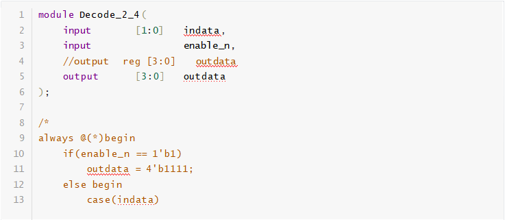
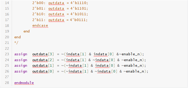
Topic 6. Design a 2-4 decoder
Title 7. Design BCD decoder and input 0 ~ 9
BCD decoder is also called 4-10 line decoder
Topic 8 MOS logic gate
NAND gate: upper parallel and lower serial (PMOS at the top and NMOS at the bottom)
NOR gate: upper series and lower parallel
Inverter
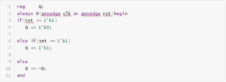
Topic 9. Draw the logic circuit with D flip-flop and the bisection circuit with synchronous high setting and asynchronous high reset terminal, which is described by Verilog
Topic 10. What are the main parts of CMOS inverter power consumption? Which factors are related?

1,P_dynamic  Is the dynamic power consumption caused by circuit Flip
2,P_short yes P Guan he N Short circuit power consumption caused by simultaneous conduction of tubes
3,P_leakage   It is the static power consumption caused by the reverse bias leakage current between the diffusion region and the substrate
 Static power consumption: CMOS When the inverter is static, P,N The tube has only one conduction. Because there is no Vdd reach GND DC Tonglu, so CMOS The static power consumption should be equal to zero. But in fact, due to the difference between the diffusion region and the substrate PN There is reverse leakage current on the junction, so it will produce static power consumption.

Short circuit power consumption: CMOS During the conversion of circuit "0" and "1", P,N The tube will conduct at the same time, producing a Vdd reach VSS Narrow pulse current, resulting in power consumption

Dynamic power consumption: C_L this CMOS The output load capacitance of the inverter is determined by NMOS and PMOS The transistor is composed of a leakage diffusion capacitor, a connecting capacitor and an input capacitor of a fan door.
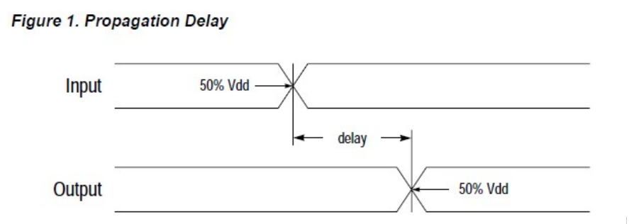
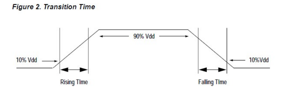
Topic 11. Definition of transition time, propagation delay and other parameters
Transition Time: input and output signals, rise time: rise time from 10%Vdd to 90%Vdd, fall time
Time L decreases from 90%Vdd to 10%Vdd. The rise time and fall time are collectively referred to as Transition Time.
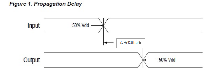
Propagation Delay: when the input signal changes to more than 50%Vdd and the output signal changes to more than 50%Vdd
Time of day.
Timing constraints include: setup time, hold time, recovery time, and minimum pulse width.
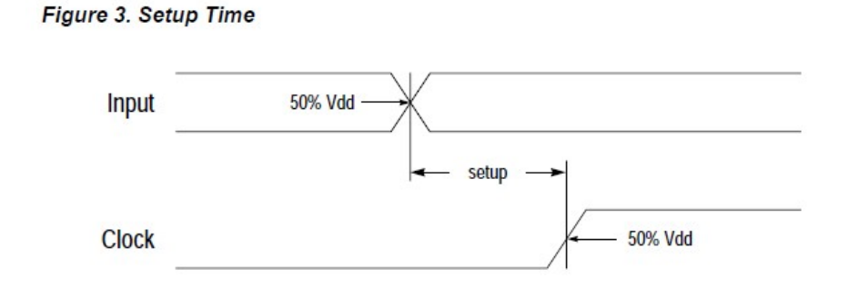
Before the arrival of the clock edge, the input signal changes by more than 50%Vdd until the clock changes by more than 50%Vdd
Minimum time of holding stability.
The minimum time for the input signal to remain stable from the time when the change of the input signal exceeds 50%Vdd after the arrival of the clock edge to the time when the change of the clock exceeds 50%Vdd.
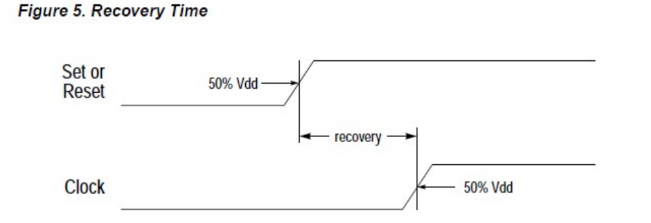
From the time when the reset or set signal changes by more than 50%Vdd to the time when the clock changes by more than 50%Vdd, the minimum time before the arrival of the clock edge ensures the completion of reset or set.
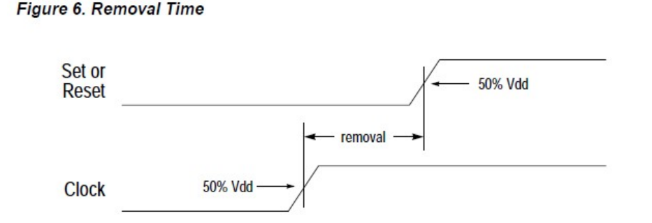
From the time when the reset or set signal changes by more than 50%Vdd to the time when the clock changes by more than 50%Vdd, the minimum time after the arrival of the clock edge ensures the completion of setting or reset.
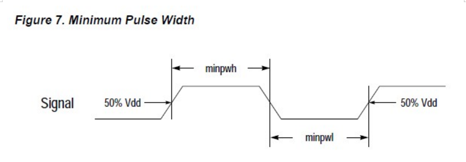
The minimum pulse width is the minimum pulse width of the high level when the rising edge of the signal changes by more than 50%Vdd to the falling edge changes by less than 50%Vdd. The same is true for the minimum width of the low level.
I personally believe that various time parameters cannot be guaranteed, which may produce metastable state.
Topic 12. Design method and idea of low power consumption in ASIC (not applicable to FPGA)
1,Reasonably plan the working mode of the chip, and control the operation of each module of the chip through the power management module Clock,Reset The purpose of controlling power consumption is achieved.
2,Gated clock( Clockgateing): Effectively reduce dynamic power consumption multi voltage power supply: reduce power consumption multi threshold voltage by controlling the voltage of the module
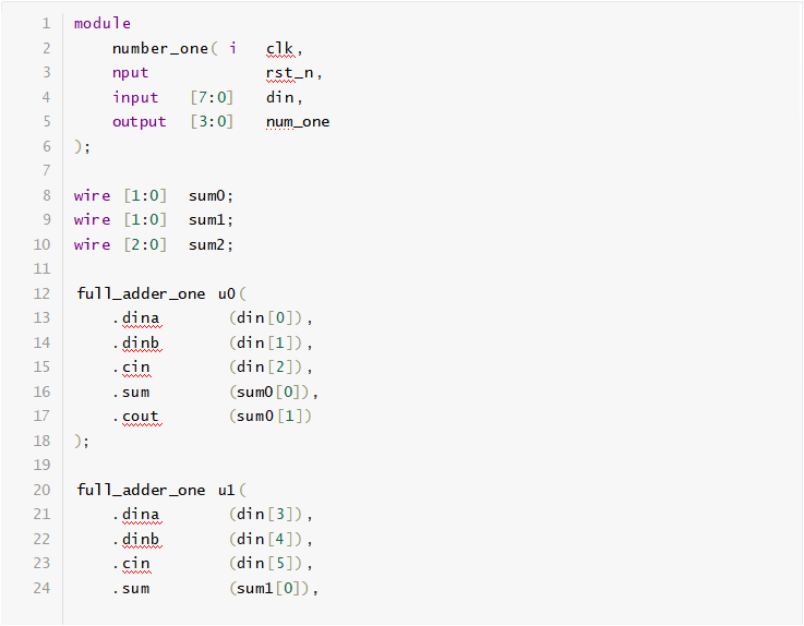
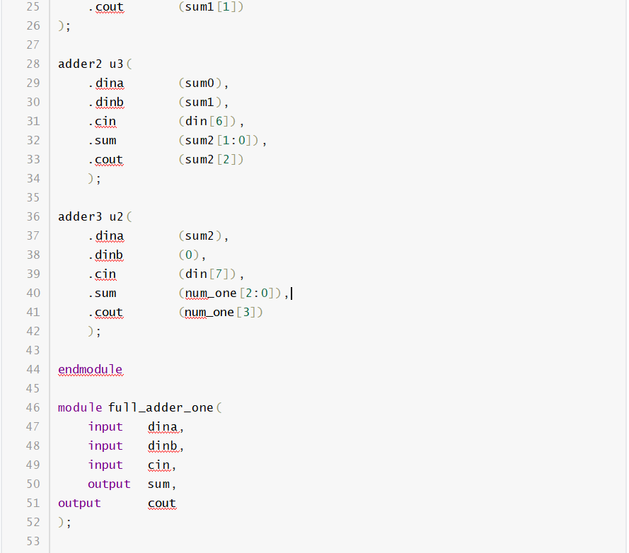
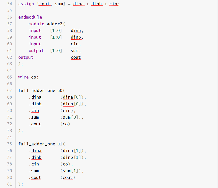
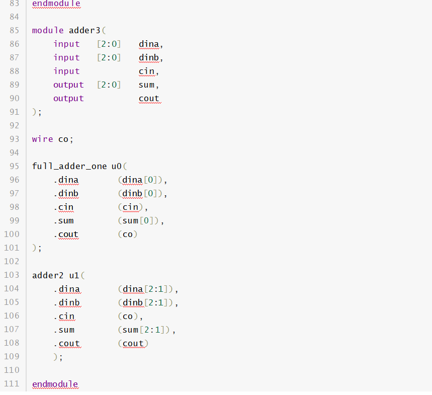
Topic 13. Input an 8-bit number and output the number of 1. If only 1 bit full adder can be used, how many are required at least?
7 1-bit full adders