I Basic characteristics of SDRAM
1. Internal memory
- bank-row-column
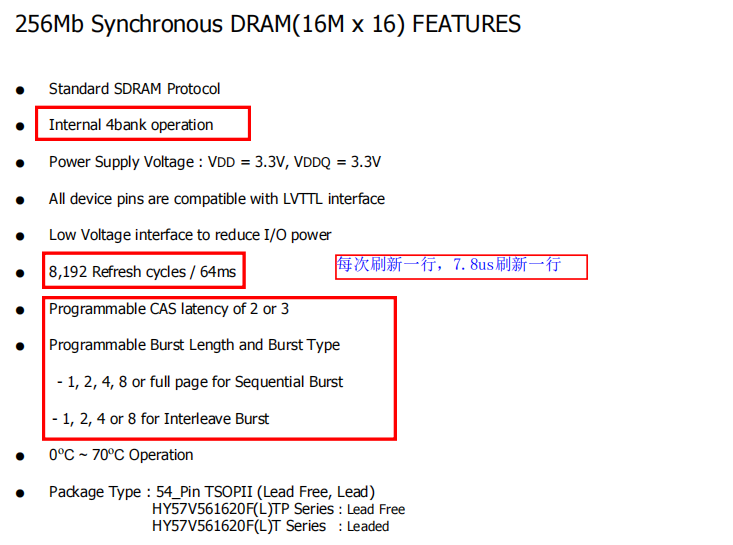
- There are four banks in total. Each bank has 213 rows and 29 columns, each of which is 16bit
2. Refresh cycle
8192refresh cycles/64ms, refresh one line every 7.8us on average
3. Introduction to data reading and writing and command sending
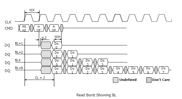
- SDRAM provides programmable read or write burst length with programmable burst length: 1, 2, 4, 8 positions or whole page. (one page represents one line)
- Data reading and writing and command sending are synchronized with the rising edge of sdram clock
- Data loss due to power failure
- Half duplex parallel communication, 16bit transmission at one time
II Pin description
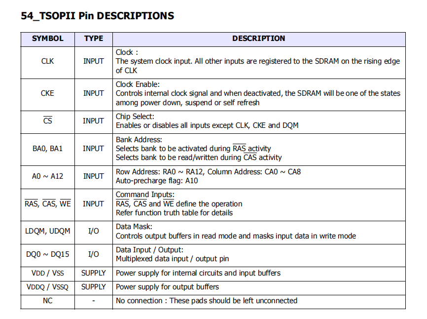
There are 13 row addresses and 9 column addresses, so each Bank=2^13 row * 2 ^ 9. One page burst represents one row burst
- CLK: the clock of SDRAM. This chip supports 133M at most, so it should be set below 133M
- CKE: clock enable signal
- CS #: SDRAM chip selection signal (# indicates that the low level is valid)
- CAS#,RAS#,WE #: these three signals constitute the command signal to SDRAM
- DQM: data input / output mask
- BA[1:0]: Bank address,
- A[12:0]: address line. When we select the row address of a Bank in SDRAM, we need to reach 13 address lines (A0 ~ A12); When col (column) is selected, only nine lines A0 ~ A8 are used; A10 this signal can be used to control auto precharge
DQ [15:0]: bidirectional data bus (three state gate)
III AC characteristic table (required delay)
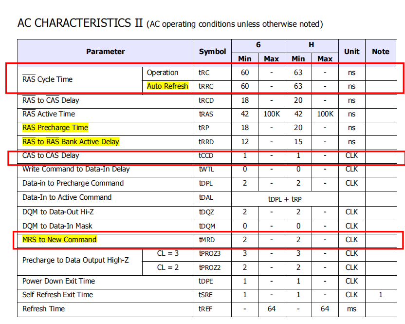
CAS:Column Address Select
RAS:Row Address Select row address
Latency: latency
Some delay time required in code
IV Mode register setting
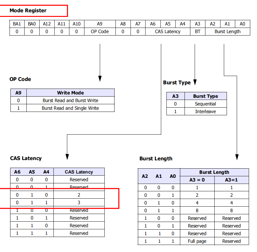
write model,burst type,CAS latency,Burst Length
- OP_MODE: burst write read / burst write single read
- CAS_LATENCY: 2 / 3 (unit: clk)
- BURST_TYPE (burst type): cannot read or write full page at 1
- BURST_LENTH (burst length): 1 / 2 / 4 / 8 / 512 (each data: 16bit)
V Command truth table, mask
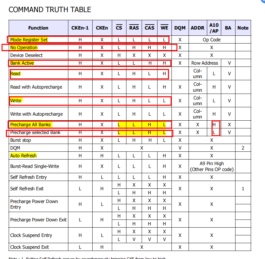
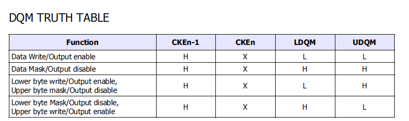
H: High level, L: low level, X: don't care
Commands needed in the code
- PRE_ALL_BANK (precharge all banks)
- AUTO_REFRSH (automatic refresh)
- MODE_ REGISTER_ Set (mode register setting)
- ROW_ Active (line activation)
- READ
- WRITE
- BURST_ Stop (both reading and writing can be terminated)
- NO_ Opration (no operation): this command will not affect the operation executed by the previous command. This command is mainly to protect the current operation from being affected
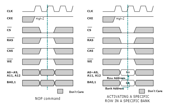
Vi Sequence diagram required
1. Write No_ OPERATION,ROW_ Sequence diagram of active command
2. Sequence diagram of reading data
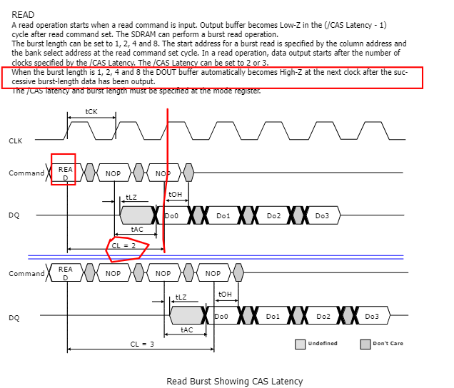
- After reading the operation command, according to the CAS set_ Latency (2 / 3clk) determines the sampling time
- After sending the read command, send the NOP command after the next rising edge
- Read data at the rising edge of each clock
3. Write data sequence diagram
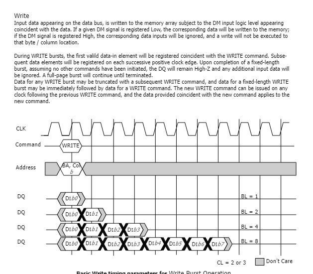
- After sending the write command, send the NOP command after the next rising edge
- Write data at the rising edge of each clock
4. Write the sequence diagram of precharge
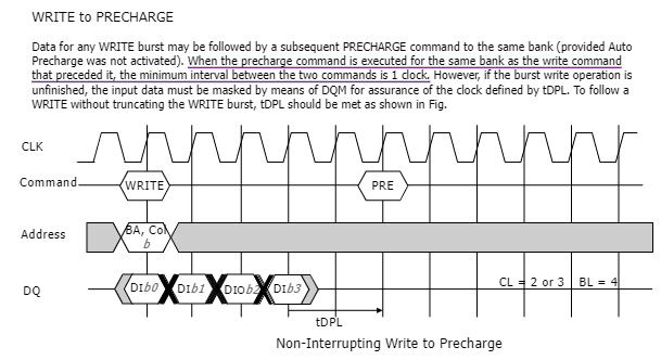
After writing the data, there is a T_ Delay of DPL
VII Code, state diagram, overall framework
1. Overall framework
2. State transition diagram
3 . code
(1) sdram_interface(sdram interface code)
module sdram_interface (
input clk ,//100sdram clock
input rst_n ,
input [15:0] write_data ,//Data written
input [1:0] req ,//Read / write request
input [14:0] mode_set ,//Select mode: a0-a10 + bank
input [23:0] addr ,//bank + row address + column address (2 + 13 + 9)
output [15:0] read_data ,//Read data
output write_data_vld,
output read_data_vld,
output cke ,//Clock enable
output cs_n ,//Chip selection, active at low level
output [1:0] bank ,//Block address
output [12:0] rc_addr ,//Row and column address setting
output ras_n ,//Line location, low level active
output cas_n ,//Column location, low level active
output we_n ,//Low level active
output [1:0] dqm ,//Mask
inout [15:0] dq //Data input and output
);
/* Parameter definition */
//State parameters
localparam POWER_ON = 10'b00000_00001,
PRE_ALL1 = 10'b00000_00010,
AUTO_REF1 = 10'b00000_00100,
MODE_SET = 10'b00000_01000,
IDLE = 10'b00000_10000,
AUTO_REF2 = 10'b00001_00000,
ROW_ACTIVE = 10'b00010_00000,
READ = 10'b00100_00000,
WRITE = 10'b01000_00000,
PRE_ALL2 = 10'b10000_00000;
//Delay parameters
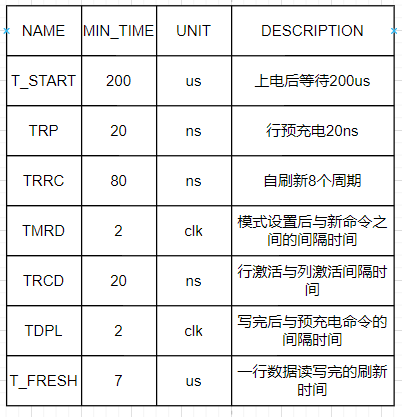
localparam T_START = 20000 ,// Wait for 200us after power on
TRP = 2 ,// Line precharge 30ns
TRRC = 8 ,// Self refresh 80ns
TMRD = 2 ,// Interval between mode setting and new command
TRCD = 2 ,// Interval between row activation and column activation
T_FRESH = 700 ,// Refresh time after reading and writing a row of data
TDPL = 2 ;// Interval between writing and precharge command
//Command parameters
localparam PRE_ALL_CMD = 4'b0010,
AUTO_REF_CMD = 4'b0001,
MODE_SET_CMD = 4'b0000,
ROW_ACTIVE_CMD = 4'b0011,
READ_CMD = 4'b0101,
WRITE_CMD = 4'b0100,
BURST_STOP_CMD = 4'b0110,
NOP_CMD = 4'b0111;
//Burst parameters
localparam BURST_LENTH_1 = 1 ,
BURST_LENTH_2 = 2 ,
BURST_LENTH_4 = 4 ,
BURST_LENTH_8 = 8 ,
BURST_LENTH_FULL = 512;//Full page burst mode, customized number of read and write sections (< = 512)
/* Signal definition */
wire [15:0] dq_in;
wire [15:0] dq_out;
wire dq_out_enable;
reg [3:0] command ; //cs_n+cas_n+ras_n+we_n
reg cke_r ;
reg [1:0] bank_r ;
reg [12:0] rc_addr_r ;
reg [1:0] dqm_r ;
reg read_req ;
reg write_req ;
reg [11:0] burst_num;//Burst length
//Counter
reg [9:0] fresh_cnt; //Row refresh counter
wire add_fresh_cnt;
wire end_fresh_cnt;
reg fresh_flag; //Meta Refresh
reg fresh_cnt_flag;//Refresh timing start flag
reg [14:0] delay_cnt; //Delay counter
wire add_delay_cnt;
wire end_delay_cnt;
reg [14:0] delay_cnt_sel;//Delay selection
reg delay_cnt_falg;//Delay start flag
reg [11:0] byte_cnt; //Byte counter
wire add_byte_cnt;
wire end_byte_cnt;
reg read_end_flag;//A flag indicating that a delay is required from the end of reading and writing
reg write_end_flag;//A flag indicating that a delay is required from the end of reading and writing
//State jump condition
wire power_preall1 ;
wire preall1_atref1;
wire atref1_modeset;
wire modeset_idle ;
wire idle_atref2 ;
wire idle_rowact ;
wire atref2_idle ;
wire rowact_read ;
wire rowact_write ;
wire read_preall2 ;
wire write_preall2 ;
wire preall2_idle ;
reg [9:0] state_c;
reg [9:0] state_n;
/* Code writing */
//state transition
always @(posedge clk or negedge rst_n)begin
if(!rst_n)begin
state_c <= POWER_ON;
end
else begin
state_c <= state_n;
end
end
//Transformation law
always @(*) begin
case(state_c)
POWER_ON :
if (power_preall1) begin
state_n = PRE_ALL1;
end
else begin
state_n = state_c;
end
PRE_ALL1 :
if (preall1_atref1) begin
state_n = AUTO_REF1;
end
else begin
state_n = state_c;
end
AUTO_REF1 :
if (atref1_modeset) begin
state_n = MODE_SET;
end
else begin
state_n = state_c;
end
MODE_SET :
if (modeset_idle) begin
state_n = IDLE;
end
else begin
state_n = state_c;
end
IDLE :
if (idle_atref2) begin
state_n = AUTO_REF2;
end
else if (idle_rowact) begin
state_n = ROW_ACTIVE;
end
else begin
state_n = state_c;
end
AUTO_REF2 :
if (atref2_idle) begin
state_n = IDLE;
end
else begin
state_n = state_c;
end
ROW_ACTIVE :
if (rowact_read) begin
state_n = READ;
end
else if (rowact_write) begin
state_n = WRITE;
end
else begin
state_n = state_c;
end
READ :
if (read_preall2) begin
state_n = PRE_ALL2;
end
else begin
state_n = state_c;
end
WRITE :
if (write_preall2) begin
state_n = PRE_ALL2;
end
else begin
state_n = state_c;
end
PRE_ALL2 :
if (preall2_idle) begin
state_n = IDLE;
end
else begin
state_n = state_c;
end
default : state_n <= state_c ;
endcase
end
//Conversion conditions
assign power_preall1 = state_c == POWER_ON && end_delay_cnt;
assign preall1_atref1 = state_c == PRE_ALL1 && end_delay_cnt;
assign atref1_modeset = state_c == AUTO_REF1 && end_delay_cnt;
assign modeset_idle = state_c == MODE_SET && end_delay_cnt;
assign idle_atref2 = state_c == IDLE && fresh_flag;
assign idle_rowact = state_c == IDLE && (read_req || write_req);
assign atref2_idle = state_c == AUTO_REF2 && end_delay_cnt;
assign rowact_read = state_c == ROW_ACTIVE && end_delay_cnt && read_req;
assign rowact_write = state_c == ROW_ACTIVE && end_delay_cnt && write_req;
assign read_preall2 = state_c == READ && end_delay_cnt;
assign write_preall2 = state_c == WRITE && end_delay_cnt;
assign preall2_idle = state_c == PRE_ALL2 && end_delay_cnt;
//fresh counter
always @(posedge clk or negedge rst_n)begin
if(!rst_n)begin
fresh_cnt <= 0;
end
else if (atref2_idle) begin
fresh_cnt <= 0;//Row refresh count regression 0
end
else if(add_fresh_cnt)begin
if(end_fresh_cnt)begin
fresh_cnt <= 0;
end
else begin
fresh_cnt <= fresh_cnt + 1;
end
end
else begin
fresh_cnt <= fresh_cnt;
end
end
assign add_fresh_cnt = fresh_cnt_flag;
assign end_fresh_cnt = add_fresh_cnt && fresh_cnt == T_FRESH - 1;
//fresh_flag
always @(posedge clk or negedge rst_n)begin
if(!rst_n)begin
fresh_flag <= 0;
end
else if(end_fresh_cnt)begin
fresh_flag <= 1'b1;
end
else if (idle_atref2) begin
fresh_flag <= 1'b0;
end
end
//fresh_cnt_flag
always @(posedge clk or negedge rst_n)begin
if(!rst_n)begin
fresh_cnt_flag <= 0;
end
else if(modeset_idle)begin
fresh_cnt_flag <= 1'b1;
end
end
//delay counter
always @(posedge clk or negedge rst_n)begin
if(!rst_n)begin
delay_cnt <= 0;
end
else if(add_delay_cnt)begin
if(end_delay_cnt)begin
delay_cnt <= 0;
end
else begin
delay_cnt <= delay_cnt + 1;
end
end
else begin
delay_cnt <= delay_cnt;
end
end
assign add_delay_cnt = delay_cnt_falg;
assign end_delay_cnt = add_delay_cnt && delay_cnt ==delay_cnt_sel - 1 ;
//delay_cnt_sel delay time selection
always @(posedge clk or negedge rst_n)begin
if(!rst_n)begin
delay_cnt_sel <= 0;
end
else if(state_c == POWER_ON )begin
delay_cnt_sel <= T_START;
end
else begin
case(state_c)
PRE_ALL1 : delay_cnt_sel <= TRP ;
AUTO_REF1 : delay_cnt_sel <= TRRC ;
MODE_SET : delay_cnt_sel <= TMRD ;
AUTO_REF2 : delay_cnt_sel <= TRRC ;
ROW_ACTIVE : delay_cnt_sel <= TRCD ;
READ : delay_cnt_sel <= TRP ;
WRITE : delay_cnt_sel <= TDPL ;
PRE_ALL2 : delay_cnt_sel <= TRP ;
default : delay_cnt_sel <= TRP ;
endcase
end
end
//delay_cnt_falg delay start flag
always @(posedge clk or negedge rst_n)begin
if(!rst_n)begin
delay_cnt_falg <= 0;
end
else if(state_n == POWER_ON || state_n == PRE_ALL1 || state_n ==AUTO_REF1 || state_n == MODE_SET)begin
delay_cnt_falg <= 1'b1;
end
else if (state_n == ROW_ACTIVE) begin
delay_cnt_falg <= 1'b1;
end
else if(state_n == PRE_ALL2 )begin
delay_cnt_falg <= 1'b1;
end
else if (state_n == READ && read_end_flag) begin
delay_cnt_falg <= 1'b1;
end
else if (state_n == WRITE && write_end_flag) begin
delay_cnt_falg <= 1'b1;
end
else if (state_n ==AUTO_REF2 ) begin
delay_cnt_falg <= 1'b1;
end
else begin
delay_cnt_falg <= 1'b0;
end
end
//cas_latency,byte_cnt, number of bytes = number of read and write sections + cas_lastency
always @(posedge clk or negedge rst_n)begin
if(!rst_n)begin
byte_cnt <= 0;
end
else if (preall2_idle) begin
byte_cnt <= 0;
end
else if(add_byte_cnt)begin
if(end_byte_cnt)begin
byte_cnt <= 0;
end
else begin
byte_cnt <= byte_cnt + 1;
end
end
else begin
byte_cnt <= byte_cnt;
end
end
assign add_byte_cnt = state_c == READ || state_c == WRITE;
assign end_byte_cnt = add_byte_cnt && byte_cnt == 525;
//read_end_flag.write_end_flag
always @(posedge clk or negedge rst_n)begin
if(!rst_n)begin
read_end_flag <= 0;
write_end_flag <= 0;
end
else if(state_c == READ && byte_cnt == burst_num - 1+2 )begin
read_end_flag <= 1'b1;
end
else if(state_c == WRITE && byte_cnt == burst_num - 1)begin
write_end_flag <= 1'b1;
end
else if (write_preall2) begin
write_end_flag <= 1'b0;
end
else if(read_preall2 )begin
read_end_flag <= 1'b0;
end
end
//burst_num
always @(posedge clk or negedge rst_n)begin
if(!rst_n)begin
burst_num <= 1;
end
else begin
case (mode_set[2:0])
3'b000 : burst_num = BURST_LENTH_1 ;
3'b001 : burst_num = BURST_LENTH_2 ;
3'b010 : burst_num = BURST_LENTH_4 ;
3'b011 : burst_num = BURST_LENTH_8 ;
3'b111 : burst_num = BURST_LENTH_FULL;
default : burst_num = 1;
endcase
end
end
//command
always @(posedge clk or negedge rst_n)begin
if(!rst_n)begin
command <= NOP_CMD;
end
else if (atref1_modeset) begin
command <= MODE_SET_CMD;
end
else if(power_preall1 || read_preall2 || write_preall2)begin
command <= PRE_ALL_CMD;
end
else if((state_c == WRITE && byte_cnt == burst_num - 1))begin
command <= BURST_STOP_CMD;
end
else if(idle_atref2 ||preall1_atref1)begin
command <= AUTO_REF_CMD;
end
else if (idle_rowact) begin
command <= ROW_ACTIVE_CMD;
end
else if (rowact_read ) begin
command <= READ_CMD;
end
else if (rowact_write ) begin
command <= WRITE_CMD;
end
else begin
command <= NOP_CMD;
end
end
//read_data, data read from sdram
assign read_data = (state_c == READ && byte_cnt >= 2 && byte_cnt <= burst_num - 1 +2)?dq_in:1'b0;
assign read_data_vld = (state_c == READ && byte_cnt >= 2 && byte_cnt <= burst_num - 1+2 )?1'b1:1'b0;
assign write_data_vld = (state_c == WRITE && byte_cnt <= burst_num - 1)?1'b1:1'b0;
assign dq_out = (state_c == WRITE && byte_cnt <= burst_num - 1)?write_data:1'b0;
assign dq_out_enable = (state_c == WRITE && byte_cnt <= burst_num - 1)?1'b1:1'b0;
//read_req,write_req
always @(posedge clk or negedge rst_n)begin
if(!rst_n)begin
read_req <= 0;
write_req <= 0;
end
else if(req[1])begin
read_req<=1'b1;
end
else if(req[0])begin
write_req<=1'b1;
end
else if (read_preall2 || write_preall2)begin
read_req <= 0;
write_req <= 0;
end
end
//bank_r,rc_addr_r
always @(posedge clk or negedge rst_n)begin
if(!rst_n)begin
bank_r <= 0;
rc_addr_r <=0;
end
else if (atref1_modeset) begin
bank_r <= mode_set[14:13];
rc_addr_r <= mode_set[12:0];
end
else if(idle_rowact)begin
bank_r <= addr[23:22];
rc_addr_r <= addr[21:9];
end
else if (rowact_read || rowact_write) begin
rc_addr_r <= {4'b0,addr[8:0]};
end
end
//dq
assign dq_in = dq;
assign dq = dq_out_enable?dq_out:1'bz;
//Interface with sdram
assign cke = 1'b1;
assign cs_n = command[3] ;
assign bank = bank_r ;
assign rc_addr = rc_addr_r ;
assign ras_n = command[2] ;
assign cas_n = command[1] ;
assign we_n = command[0] ;
assign dqm = 2'b00;//No need to hide data
endmodule //sdram_interface
(2). sdram_ctrl(sdram control module code)
module sdram_ctrl (
    input              clk         ,
    input              rst_n       ,
    input  [1:0]       key_down    ,//Key

    output     [15:0]  write_data  ,//Output: signal of interface module
    output reg [1:0]   req         ,
    output reg [14:0]  mode_set    ,
    output reg [23:0]  addr        ,
    output             clk_100m    ,

    input   [15:0]     read_data   ,//Input: signal of interface module
    input              write_data_vld,
    input              read_data_vld,

//UART_TX signal
    input              busy        ,
    output    [7:0]    tx_data     ,//Incoming uart_tx data
    output             tx_data_vld ,
//UART_RX signal
    input   [7:0]      rx_data     ,//input data
    input              rx_data_vld

);


/* Parameter definition */
//MODE_SET mode setting parameters
localparam    OP_MODE     =  1'b0  ,//Write mode control
              CAS_LATENCY =  3'b010,//Column location delay
              BURST_TYPE  =  1'b0  ,//Burst type
              BURST_LENTH =  3'b111;//Burst length

//Read write address
localparam    RW_ADDR     = 16'h0;


pll_100m	pll_100m_inst (
	.areset ( ~rst_n ),
	.inclk0 ( clk),
	.c0 ( clk_100m )
);

//req
always @(posedge clk or negedge rst_n)begin
    if(!rst_n)begin
        req <= 2'b0;
    end
    else if(key_down[1])begin
        req[1] =1'b1;
    end
    else if(key_down[0])begin
        req[0] =1'b1;
    end
    else begin
        req <= 2'b0;
    end
end


//mode_set
always @(posedge clk or negedge rst_n)begin
    if(!rst_n)begin
        mode_set <= 0;
    end
    else begin
        mode_set <= {5'b0,OP_MODE,2'b0,CAS_LATENCY,BURST_TYPE,BURST_LENTH};
    end
end

//addr
always @(posedge clk or negedge rst_n)begin
    if(!rst_n)begin
        addr <= 16'h0;
    end
    else begin
        addr <= RW_ADDR;
    end
end


/* fifo */
//write_fifo from UART_RX receives data written to sdram
write_fifo	write_fifo_inst (
	.aclr                   ( ~rst_n        ),
	.data                   ( wfifo_data_in ),
	.rdclk                  ( clk_100m      ),
	.rdreq                  ( wfifo_rdreq   ),
	.wrclk                  ( clk           ),
	.wrreq                  ( wfifo_wrreq   ),
	.q                      ( wfifo_data_out),
	.rdempty                ( wfifo_rdempty ),
	.rdfull                 ( wfifo_rdfull  ),
	.rdusedw                ( wfifo_rdusedw ),
	.wrempty                ( wfifo_wrempty ),
	.wrfull                 ( wfifo_wrfull  ),
	.wrusedw                ( wfifo_wrusedw )
	);
//wfifo read signal
wire        wfifo_rdreq     ;
wire [15:0] wfifo_data_out  ;
wire        wfifo_rdempty   ;
wire        wfifo_rdfull    ;
wire [11:0]  wfifo_rdusedw   ;
//Signal written by wfifo
wire [15:0] wfifo_data_in   ;
wire        wfifo_wrreq     ;
wire        wfifo_wrempty   ;
wire        wfifo_wrfull    ;
wire [11:0]  wfifo_wrusedw   ;

//Write wfifo
assign      wfifo_wrreq = rx_data_vld && ~wfifo_wrfull;
assign      wfifo_data_in = rx_data;

//Read fifo data to sdram
assign      wfifo_rdreq =  ~wfifo_rdempty && write_data_vld;
assign      write_data  = wfifo_data_out ;


//read_fifo reads data from sdram and transfers it to UART_TX
read_fifo	read_fifo_inst (
	.aclr                   ( ~rst_n        ),
	.data                   ( rfifo_data_in ),
	.rdclk                  ( clk           ),
	.rdreq                  ( rfifo_rdreq   ),
	.wrclk                  ( clk_100m      ),
	.wrreq                  ( rfifo_wrreq   ),
	.q                      ( rfifo_data_out),
	.rdempty                ( rfifo_rdempty ),
	.rdfull                 ( rfifo_rdfull  ),
	.rdusedw                ( rfifo_rdusedw ),
	.wrempty                ( rfifo_wrempty ),
	.wrfull                 ( rfifo_wrfull  ),
	.wrusedw                ( rfifo_wrusedw )
	);


//rfifo read signal
wire        rfifo_rdreq     ;
wire [15:0] rfifo_data_out  ;
wire        rfifo_rdempty   ;
wire        rfifo_rdfull    ;
wire [11:0]  rfifo_rdusedw   ;
//Signal written by rfifo
wire [15:0] rfifo_data_in   ;
wire        rfifo_wrreq     ;
wire        rfifo_wrempty   ;
wire        rfifo_wrfull    ;
wire [11:0]  rfifo_wrusedw   ;


//Write fifo
assign   rfifo_wrreq = read_data_vld && ~wfifo_wrfull ;
assign   rfifo_data_in =read_data;

//Read rfifo data to uart_tx
assign rfifo_rdreq =  ~busy && ~rfifo_rdempty;
assign tx_data_vld = rfifo_rdreq;
assign tx_data     = rfifo_data_out;
endmodule //sdram_ctrl
(3). Top (top level code)
module top (
    input              clk      ,
    input              rst_n    ,

    input     [1:0]    key_in   ,
//Serial port interface
    input              uart_rxd ,
    output             uart_txd ,
//sdram interface
    output             clk_100m ,
    output             cke      ,
    output             cs_n     ,
    output    [1:0]    bank     ,
    output    [12:0]   rc_addr  ,
    output             ras_n    ,
    output             cas_n    ,
    output             we_n     ,
    output    [1:0]    dqm      ,
    inout     [15:0]   dq

);
//sdram_ctrl and sdram_interface connected signal
wire [15:0]     write_data;//Data written to sdram
wire [1:0]      req       ;//Read / write request
wire [14:0]     mode_set  ;//sdram mode setting
wire [23:0]     addr      ;//bank + row + column address


//sdram_interface and sdram_ctrl connected signal
wire [15:0]     read_data ;//Data read from sdram
wire [1:0]      key_down  ;//Key detection
(* keep *) wire            write_data_vld;
(* keep *) wire            read_data_vld ;

//Signal of serial port and sdram connection
wire                 busy       ;//Serial port is transmitting data
wire      [7:0]      rx_data    ;//Data received by serial port
wire                 rx_data_vld;//Received data valid
wire      [7:0]      tx_data    ;//Serial data transmission
wire                 tx_data_vld;//Serial port transmission data is valid

uart_rx u_uart_rx(
    /* input           */     .clk        (clk        ) ,
    /* input           */     .rst_n      (rst_n      ) ,
    /* input           */     .uart_rxd   (uart_rxd   ) ,
    /*     */
    /* output   [7:0]  */     .rx_data    (rx_data    ) ,
    /* output          */     .rx_data_vld(rx_data_vld)

);

uart_tx u_uart_tx(
    /* input          */      .clk        (clk        ) ,
    /* input          */      .rst_n      (rst_n      ) ,
    /* input    [7:0] */      .tx_data    (tx_data    ) ,
    /* input          */      .tx_data_vld(tx_data_vld) ,

    /* output         */      .busy       (busy       ) ,
                              .uart_txd   (uart_txd   )

);

//sdram_ctrl
sdram_ctrl u_sdram_ctrl(
    /* input             */  .clk       (clk       )            ,
    /* input             */  .rst_n     (rst_n     )            ,
    /* input  [1:0]      */  .key_down  (key_down  )            ,//Key

    /* output reg [15:0] */  .write_data(write_data)            ,//Output: signal of interface module
    /* output reg [1:0]  */  .req       (req       )            ,
    /* output reg [14:0] */  .mode_set  (mode_set )             ,
    /* output reg [23:0] */  .addr      (addr      )            ,
    /* output            */  .clk_100m  (clk_100m  )            ,

    /* input   [15:0]    */  .read_data (read_data )            ,//Input: signal of interface module
                            .write_data_vld(write_data_vld)     ,
                            .read_data_vld(read_data_vld)       ,
    /*  */
    /*  */
    /* //UART_TX signal */
    /*     input         */ .busy       (busy       ) ,
    /*     output  [7:0] */ .tx_data    (tx_data    ) ,//Incoming uart_tx data
    /*     output        */ .tx_data_vld(tx_data_vld) ,
    /* //UART_RX signal */
    /*     input   [7:0] */ .rx_data    (rx_data    ) ,//input data
    /*     input         */ .rx_data_vld(rx_data_vld)


);


//sdram_interface
sdram_interface u_sdram_interface(
    /* input             */  .clk       (clk_100m  )        ,//100sdram clock
    /* input             */  .rst_n     (rst_n     )        ,
    /* input     [15:0]  */  .write_data(write_data)        ,//Data written
    /* input     [1:0]   */  .req       (req       )        ,//Read / write request
    /* input     [14:0]  */  .mode_set (mode_set )          ,//Mode selection: bank+A0-A10
    /* input     [23:0]  */  .addr      (addr      )        ,//bank + row address + column address (2 + 13 + 9)
    /* output    [15:0]  */  .read_data (read_data )        ,//Read data
                             .write_data_vld(write_data_vld),
                             .read_data_vld(read_data_vld)  ,

    /* output            */  .cke       (cke       )        ,//Clock enable
    /* output            */  .cs_n      (cs_n      )        ,//Chip selection, active at low level
    /* output    [1:0]   */  .bank      (bank      )        ,//Block address
    /* output    [12:0]  */  .rc_addr   (rc_addr   )        ,//Row and column address setting
    /* output            */  .ras_n     (ras_n     )        ,//Line location, low level active
    /* output            */  .cas_n     (cas_n     )        ,//Column location, low level active
    /* output            */  .we_n      (we_n      )        ,//Low level active
    /* output    [1:0]   */  .dqm       (dqm       )        ,//Mask
    /* inout     [15:0]  */  .dq        (dq        )        //Data input and output


);


key_debounce u_key_debounce (
        /* 	input					 */.clk		(clk	),
        /* 	input					 */.rst_n	(rst_n	),
        /* 	input		[KEY_W-1:0] */ .key_in  (key_in ),
        /* 	 */
        /* 	output	reg	[KEY_W-1:0] */ .key_out (key_down)	 //When pressing is detected, a cycle of high pulse is output, and other times are 0
);
endmodule //top