Target Reflected Echo Detection Algorithms and Their Implementation on FPGA Part 3:
Top-level Implementation of Square and Integral Circuits and Algorithms
Some time ago, I came into contact with a project of sonar target echo detection. The core function of sonar receiver is to recognize the echo of the excitation signal emitted by the transmitter in the reflected echo which contains a lot of noise. I will share the development process and code of this echo recognition algorithm based on FPGA in several articles. Welcome your comments. The following original content is welcomed to be reproduced by netizens, but please indicate the source: https://www.cnblogs.com/helesheng.
In the first part of this series of blogs, based on the simulation results, I believe that the method of calculating target distance by using the results of "cross correlation of reflected echo and excitation signal" has high performance and computational efficiency. In the second blog post in this series, I implemented data cross-correlation/convolution/FIR filter calculation using a semi-parallel "dual-memory convolution section" structure in the low-cost FPGA of Cyclone series. As the third blog article in this series, I will implement the square sum integral calculation of cross-correlation signals, and combine all the algorithms in the top-level file as a whole.

By looking for  The location of the extreme point of the target reflector is used to determine the time point when the target reflects the echo.
In Formula (1) It is the part of cross-correlation algorithm, and its implementation on FPGA has been introduced in the previous paper. According to the symbols defined above, the discretized cross-correlation signal is recorded as R[k]. After further discretization, (1) can be rewritten to the following form that can be implemented by FPGA:

1. Realization of Square Circuit
Using MegaWizard in Quartus-II to configure the square computing circuit, the structure is shown in the following figure.
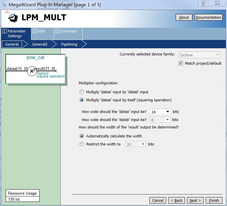
Figure 1 Square Circuit Configuration
II. Design of Integral Circuit
According to formula (2), in order to calculate the value of objective function P[n], it is necessary to sum (integrate) the historical values. Of course, we can use buffers to store historical k0 values and sum the k0 values in the buffers before each output. If k0 is equal to the length of the excitation signal N, then N-1 addition must be calculated before each output P[n]. When N is 64 (as mentioned earlier), this is almost an impossible task. I designed the circuit structure shown in the following figure to achieve the summation of 64 historical data.
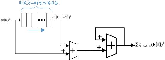
Figure 2 Integrator Circuit Structure
One of the 64-depth shift registers serves to provide "historical data" before 64 samples. First, the current data And the oldest historical data
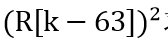 Find the difference (complement), and then sum the difference continuously. In this way, according to the law of addition and exchange, the final summation result is equivalent to adding the current data, subtracting the oldest historical data. As long as the initial value of the shift register is all 0, after 64 operations, the sum (integral) of 64 historical data is obtained from the output. The shift register configuration with MegaWizard is shown in the following figure.
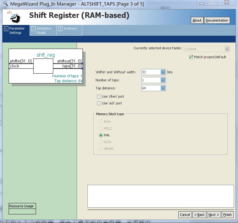
Figure 3 Structure of shift register
The structure of the former subtractor is shown in the following figure.
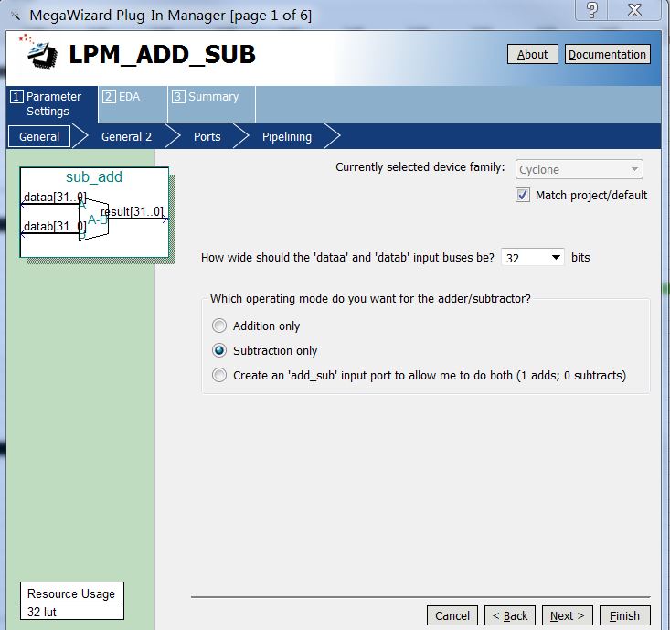
Figure 4 Structure of subtractor
The accumulator is implemented in hardware description language with the following code.
1 always @ (posedge start or negedge rst_n)
2 begin
3     if(!rst_n)
4         acc_out[39:0] <= 40'd0;
5     else begin
6         acc_out[39:0] = $signed(acc_out[39:0]) + $signed(acc_in[31:0]);
7     end
8 end
The keyword $signed denotes an adder with signed numbers.
3. Top-level design of algorithm
In order to connect the aforementioned A/D and D/A control circuit, cross-correlation/convolution/FIR filter circuit and square-sum integral circuit into one system, it is necessary to exemplify and connect the above module circuits in the top-level design documents. In addition, the top-level design document will also control the overall working schedule of the system. The top-level file I designed is shown below.
  1 module CONV_POW_AD_DA(
  2 ///////////Top-level module, responsible for calling ADC to collect data, convolute, and then output the results of convolution/FIR with DAC/////////
  3     input rst_n,//Low level reset signal
  4     input iclk20,//External crystal input 20 MHz
  5     output sck_da,//D/A Converter SPI Clock
  6     output mosi_da,//D/A Converter SPI data signal
  7     output cs_da,//D/A Chip Selection Signal of Converter
  8     output ld_da,//D/A Dual Channel Data Loading Signal of Converter
  9     output sck_ad,//A/D Converter SPI Clock
 10     output mosi_ad,//A/D Converter SPI data output
 11     input miso_ad,////A/D Converter SPI data input
 12     output cs_ad//A/D Converter SPI Mouth Selection Signal
 13     );
 14      wire clk;
 15   reg start;
 16   reg[15:0] cnt;//A timer used to generate the overall cycle
 17      reg[11:0] tst_data;//Counter for generating test data
 18   parameter CNT_NUM = 16'd2000;//At 100M clock, 2000 frequency division means 50KHz overflow rate
 19   wire[11:0] ad_data;//AD Internal connection of conversion results
 20   wire[11:0] data_cha;//A Channel data
 21   wire[11:0] data_chb;//B Channel data
 22      wire[15:0] shft_data1;//Data passed between two sections of convolution
 23      wire[15:0] shft_data2;//Data passed between two sections of convolution
 24      wire[15:0] shft_data3;//Data passed between two sections of convolution
 25      wire[15:0] shft_data4;//Data passed between two sections of convolution
 26      wire[39:0] conv_res1;//The results of convolution in Section I
 27      wire[39:0] conv_res2;//CONVOLUTION RESULTS IN SECTION 2
 28      wire[39:0] conv_res3;//CONVOLUTION RESULTS IN SECTION 3
 29      wire[39:0] conv_res4;//CONVOLUTION RESULTS IN SECTION 4
 30      wire[39:0] conv_res;//The result of total convolution
 31      wire[33:0] acc_sum;//Finally, the cumulative sum of each section is calculated.
 32      wire[31:0] shiftout;//Removal data from shift registers
 33      wire[15:0] ac_sig;//AC signal after removal of DC bias
 34      wire[31:0] pow_sig;//Energy of signal
 35      wire signed[31:0] acc_in;//The input of a summation accumulator is also an addition./Output of subtractor
 36      reg signed[39:0] acc_out;//The output of the accumulator
 37      wire signed[19:0] data_out;//Output of Cumulative Results after Cumulative Formulation
 38
 39      //assign data_cha[11:0] = acc_out[25:14];//passageway a Output 64 Point Energy Accumulation Results
 40      //assign data_cha[11:0] = shiftout[18:7];//passageway a Output data
 41      assign data_cha[11:0] = pow_sig[19:8];//passageway a Square of output AC signal
 42      //assign data_cha[11:0] = ad_data[11:0];//passageway a Output data
 43      //assign data_cha[11:0] = shft_data2[11:0];//passageway a Output data
 44      //assign data_chb[11:0] = conv_res[26:15];//passageway b Output data
 45      //The coefficient itself is 16. bit Symbolic, as FIR If the sum of the coefficients of the filter is 1, then 16 bits The sum of all the signed coefficients is 32768.
 46      //Therefore, it is necessary to shift the filtering result to the right by 15. bit,So take 26 of the results.:15. But because of DA Reference voltage 2.048V,less than AD 3.3V So the filtering result is still slightly smaller.
 47      //assign data_chb[11:0] = data_out[14:3];//passageway b Output cumulative result prescription
 48      assign data_chb[11:0] = acc_out[28:17];//passageway b Output 64 Point Energy Accumulation Results
 49      //assign data_chb[11:0] = pow_sig[20:9];//passageway b Square of output AC signal
 50      //assign data_chb[11:0] = acc_sum[26:15];//passageway b Output filtering/Convolution results
 51      //assign data_chb[11:0] = conv_res1[26:15];//passageway b Output data
 52
 53      /////Connections used in the following coefficient configurations/////
 54      wire rdy_work;//Configuration Completion Signal, High Level Indicates Configuration Completion
 55      wire[7:0] wr_blk_addr;//Backward Coefficient blk Configured address
 56      wire[15:0] data_bank;//Directional coefficients blk Configured data
 57      wire csh0,csh1,csh2,csh3;//Coefficient allocated for each section blk Gating line
 58      PLL20_100 i_pll20_100(//Instantiation PLL Clock generation
 59         .inclk0(iclk20),
 60         .c0(clk)//pll Output 100 M Working clock
 61         );
 62
 63    always @ (posedge clk or negedge rdy_work)
 64     begin
 65         if(!rdy_work)
 66         begin
 67             start <= 1'd0;
 68             cnt[15:0] <= 16'd0;
 69                 tst_data[11:0] <= 12'd0;        //Counters for testing
 70         end
 71         else begin
 72             //////////Maintenance Period Counter///////////
 73             if(cnt < CNT_NUM-1) begin
 74                 cnt[15:0] <= cnt[15:0] + 16'd1;
 75                      tst_data[11:0] <= tst_data[11:0];
 76                 end
 77             else begin
 78                 cnt[15:0] <= 16'd0;
 79                      tst_data[11:0] <= tst_data[11:0] + 12'd1;        //Counters for testing
 80                 end
 81
 82             ////////Generate startup signal/////
 83             if((cnt > 102)&(cnt <= 105))//In 105th clk Generate startup signal
 84                 start <= 1'D1;//Start MCP4822 Output State Machine
 85             else
 86                 start <= 1'D0;
 87         end
 88     end
 89
 90      init_coe_blk i_init_coe_blk(//The instantiation coefficient configuration module reads the coefficients from the coefficient pool and directs them to the coefficients. blk The function of configuring data is only valid at the beginning of reset. ready Signal Control Subsequent Module
 91                     .clk(clk),
 92                     .rst_n(rst_n),//Overall reset signal
 93                     .ready(rdy_work),//Configuration Completion Signal, High Level Indicates Configuration Completion
 94                     .wr_blk_addr(wr_blk_addr),//Backward Coefficient blk Configured address
 95                     .data_bank(data_bank),//Directional coefficients blk Configured data
 96                     .csh0(csh0),//Section I Coefficient of Allocation blk Gating line
 97                     .csh1(csh1),//Section II Coefficient of Allocation blk Gating line
 98                     .csh2(csh2),//Section 3 Coefficient of Allocation blk Gating line
 99                     .csh3(csh3)//Section IV Coefficient of Allocation blk Gating line
100                     );
101
102     CONV_SER16 i_conv_ser16_I(//Instantiate the first 16-order convolution/fir Circuit
103                     .clk(clk),
104                     .a({4'd0,ad_data}),//AD conversion results as data input
105                     //.a({4'd0,tst_data[11:0]}),//AD Transform results as data input
106                     .en(rdy_work),//Coefficient configuration is completed before enabling
107                     .coe_data_in16(data_bank),//Initialization Coefficient Data Input
108                     .wr_coe_addr(~wr_blk_addr[3:0]),//Address Input of Initialization Coefficient
109                     ////!!!Particular attention is paid here to the fact that the multiply-add data enters the multiply-add operation from the large address, so the address requires a complement to flip the coefficients. Amount to: fliplr();!!!!!//
110                     .wr_coe_clk(clk),//Initialization Coefficient Writing Clock
111                     .wr_coe_en(csh0),//The enabler of coefficient configuration is generated by address decoding of initialization module, which facilitates different coefficients. blk Gating
112                     .start(start),//Input Start Convolution Sum fir Control end
113                     //.shft_out_dp_data(),
114                     .shft_out_dp_data(shft_data1[15:0]),
115                     //.s_latch(conv_res)
116                     .s_latch(conv_res1[39:0])
117                     );
118     CONV_SER16 i_conv_ser16_II(//Instantiate the second 16-order convolution/fir Circuit
119                     .clk(clk),
120                     .a(shft_data1[15:0]),//Data removed from the first section of the cascade
121                     .en(rdy_work),//Coefficient configuration is completed before enabling
122                     .coe_data_in16(data_bank),//Initialization Coefficient Data Input
123                     .wr_coe_addr(~wr_blk_addr[3:0]),//Address Input of Initialization Coefficient
124                     ////!!!Particular attention is paid here to the fact that the multiply-add data enters the multiply-add operation from the large address, so the address requires a complement to flip the coefficients. Amount to: fliplr();!!!!!//
125                     .wr_coe_clk(clk),//Initialization Coefficient Writing Clock
126                     .wr_coe_en(csh1),//The enabler of coefficient configuration is generated by address decoding of initialization module, which facilitates different coefficients. blk Gating
127                     .start(start),//Input Start Convolution Sum fir Control end
128                     .shft_out_dp_data(shft_data2[15:0]),
129                     .s_latch(conv_res2[39:0])
130                     );
131     CONV_SER16 i_conv_ser16_III(//Instantiate the third 16-order convolution/fir Circuit
132                     .clk(clk),
133                     .a(shft_data2[15:0]),//Data removed from the first section of the cascade
134                     .en(rdy_work),//Coefficient configuration is completed before enabling
135                     .coe_data_in16(data_bank),//Initialization Coefficient Data Input
136                     .wr_coe_addr(~wr_blk_addr[3:0]),//Address Input of Initialization Coefficient
137                     ////!!!Particular attention is paid here to the fact that the multiply-add data enters the multiply-add operation from the large address, so the address requires a complement to flip the coefficients. Amount to: fliplr();!!!!!//
138                     .wr_coe_clk(clk),//Initialization Coefficient Writing Clock
139                     .wr_coe_en(csh2),//The enabler of coefficient configuration is generated by address decoding of initialization module, which facilitates different coefficients. blk Gating
140                     .start(start),//Input Start Convolution Sum fir Control end
141                     .shft_out_dp_data(shft_data3[15:0]),
142                     .s_latch(conv_res3[39:0])
143                     );
144     CONV_SER16 i_conv_ser16_IV(//Instantiate the fourth 16-order convolution/fir Circuit
145                     .clk(clk),
146                     .a(shft_data3[15:0]),//Data removed from the first section of the cascade
147                     .en(rdy_work),//Coefficient configuration is completed before enabling
148                     .coe_data_in16(data_bank),//Initialization Coefficient Data Input
149                     .wr_coe_addr(~wr_blk_addr[3:0]),//Address Input of Initialization Coefficient
150                     ////!!!Particular attention is paid here to the fact that the multiply-add data enters the multiply-add operation from the large address, so the address requires a complement to flip the coefficients. Amount to: fliplr();!!!!!//
151                     .wr_coe_clk(clk),//Initialization Coefficient Writing Clock
152                     .wr_coe_en(csh3),//The enabler of coefficient configuration is generated by address decoding of initialization module, which facilitates different coefficients. blk Gating
153                     .start(start),//Input Start Convolution Sum fir Control end
154                     .shft_out_dp_data(shft_data4[15:0]),
155                     .s_latch(conv_res4[39:0])
156                     );
157     PADD    i_PADD (//For convenience DA Output biases all outputs to positive numbers
158                     .clock ( start ),
159                     .data0x ( conv_res1[31:0] ),
160                     .data1x ( conv_res2[31:0] ),
161                     .data2x ( conv_res3[31:0] ),
162                     .data3x ( conv_res4[31:0] ),
163                     .result ( acc_sum[33:0] )
164                     );
165
166     MCP4822 i_mcp4822(.clk100m(clk),
167                       .rst_n(rdy_work),
168                       .start(start),
169                       .dac_data_a(data_cha),//passageway a Output data
170                       //.dac_data_b(dds_data12),//passageway b Connect DDS content
171                       //.dac_data_b(product12),//passageway b High 12-bit join multiplication
172                       //.dac_data_b(conv_data12),//passageway b The result of join convolution
173                            .dac_data_b(data_chb),//passageway b Output data
174                       .cs(cs_da),
175                       .mosi(mosi_da),
176                       .sck(sck_da),
177                       .ld(ld_da)
178                       );
179     MCP3202 i_mcp3202(
180                      .clk100m(clk),
181                      .rst_n(rdy_work),
182                      .start(start),
183                      .adc_data_a(ad_data),
184                      .cs(cs_ad),
185                      .mosi(mosi_ad),
186                      .miso(miso_ad),
187                      .sck(sck_ad)
188                      );
189
190     sub_offset    i_sub_offset (//This subtractor is used from AD The result is a 16-bit complement when the DC bias is removed.
191     .dataa ( {4'd0,acc_sum[26:15]} ),//Convolution results for calculation
192     //.dataa ( {4'd0,ad_data[11:0]} ),//AD It turns out to be a positive integer, with a 16-bit complement to zero.
193     .datab ( 16'h0000 ),//DC bias is considered to be 1/2 full range 16'h0800,No DC bias is 16'h0000
194     .result ( ac_sig[15:0] )//After removing DC bias, the result is 16. bit Complement code
195     );
196
197     pow_cal    i_pow_cal (//Square operation to calculate signal energy
198     .dataa ( ac_sig[15:0] ),
199     .result ( pow_sig[31:0] )
200     );
201
202     shft_reg    i_shft_reg (//Instantiated shift register
203         .clock ( start ),
204         .shiftin ( pow_sig[31:0] ),
205         .shiftout ( shiftout[31:0] ),
206         .taps (  )
207         );
208     sub_add    sub_add_inst (//A subtractor that subtracts the number to be taken from the cumulative result by the number fed into the cumulative result. The result may be negative.
209                 //After subtraction, it is fed into the accumulator to maintain the contents of the accumulator: the sum of the latest 64
210     .dataa ( pow_sig[31:0] ),
211     .datab ( shiftout[31:0]),
212     .result ( acc_in[31:0] )
213     );
214 ////////Calculate the sum of the nearest 64 numbers/////////
215 always @ (posedge start or negedge rst_n)
216 begin
217     if(!rst_n)
218         acc_out[39:0] <= 40'd0;
219     else begin
220         acc_out[39:0] = $signed(acc_out[39:0]) + $signed(acc_in[31:0]);
221     end
222 end
223 ///////Increasing the Resolution of Small Signals by Accumulating and Reciprocating
224     ip_sqrt    ip_sqrt_inst (
225         .radical ( acc_out[39:0] ),
226         .q ( data_out[19:0] ),
227         .remainder (  )
228         );
229 endmodule
Most of the above top-level design documents are examples and connection statements of each functional module circuit. Because the code annotations are very detailed, the details will not be repeated here. I mainly introduce the following points:
1. There is only one always procedure assignment statement, which maintains the work of the counter cnt[15:0]. The total synchronous start signal is generated when cnt[15:0] is a specific value, so the period of cnt[15:0] technology also determines the period of start signal, that is, the period of signal.
2. As I prepared for this series“ Control Hardware Interface with Verilog-HDL State Machine ” The advantage of using A/D and D/A to debug the algorithm of FPGA is that the signal of each intermediate node in the algorithm can be presented through D/A converter. The assignment of data_cha[11:0] and data_chb[11:0] in the code has a large number of optional annotations, which are reserved for this reason.
3. In the instantiation code of CONV_SER16 for each convolution section, the interface wr_coe_addr is the initial write address of the coefficient memory (for the content of the initialization part of the coefficient memory, see the description in the second blog article of this series, "Implementing the cross-correlation/convolution/FIR circuit". But when connecting, wr_coe_addr reverses the address wr_blk_addr of the output of the coefficient initializer, because each convolution section multiplies the input first by the content of the coefficient memory with a larger address, so the address should be flipped. Otherwise, the complete sequence of coefficients stored in the coefficient initialization pool will be reversed in each convolution section, which will not produce the correct results.
IV. Test results
The results of FPGA synthesis for Cyclone-I in Quartus-II are shown in the following figure.
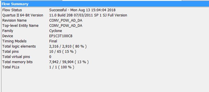
Figure 5 Results of synthesis, layout and wiring
Using matlab to generate 6 sinusoidal cycles of signals with 60 sampling points in length, two zeros are added before and after the signals, thus the sinusoidal signals with 64 sampling points in length are obtained. The reason why 60 sampling points contain 6 sinusoidal cycles is to simulate the sampling rate of 5KHz sinusoidal signal @50KSPS. Finally, the blackman window is added to 64 sampling points to reduce the impact of leakage.
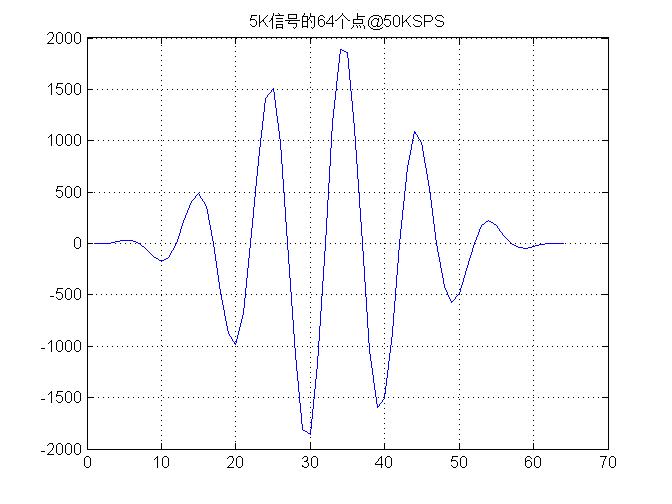
Figure 6 Ideal target reflection echo signal
I downloaded the signal to SideTech arbitrary signal generator 33521 and manually triggered 33521 to generate the waveform shown above to simulate the theoretical echo signal. Connect it to the A/D input of the FPGA platform, and output the processing results from the D/A of the FPGA platform. Observing input and processing results with an oscilloscope is shown in the following figure.
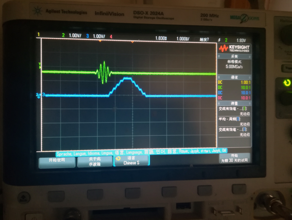
Figure 7 Processing results of field measurements
The above figure shows that the algorithm in the FPGA realizes the output waveform simulated by matlab theory in the first part of this series of blog posts, which can meet the requirements of the target echo detection algorithm. The delay of blue convolution results is due to the latency of the FPGA algorithm, which does not affect the real-time performance of the system.
Of course, what we have accomplished here is only a validation experiment of the algorithm. If we want to really use it, we need to further improve the speed of A/D and D/A conversion.
For the principle and implementation of target echo detection algorithm, please start with the beginning of this series of blog posts.[ Target Reflected Echo Detection Algorithms and Their Implementation on FPGA: An Overview of Algorithms].