Title:
According to the basic principles of classroom teaching, I try to write an IIC control logic and FPGA output
The input clock is 10MHz and the communication frequency of IIC is 400KHz. FPGA is required to write control to AD chip
System instruction, the address of AD chip is 0000123 (changed to decimal 123, i.e. 01111111), AD chip
There are three registers with consecutive addresses, the address is 0x48, the configuration data is 0x55 and the address is 0x49,
The configuration data is 0xAA, the address is 0x50, and the configuration data is 0xCC. Try to draw the circuit connection block diagram and state
State transition diagram, complete code writing and simulation.
analysis:
According to the requirements, the IIC communication module should establish a connection between FPGA and AD chip. The most important thing is that SCL clock line is output to AD chip to establish communication clock, and SDA line is used to realize bidirectional data
Data transmission.
The block diagram of circuit module is as follows:
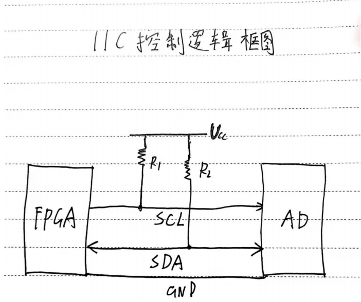
Two pull-up resistors R1 and R2 ensure that both SCL line and SDA line are protected in idle state
Hold high.
According to the communication method of IIC, we
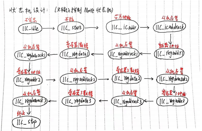
Moore state machine
The reason for timing writing is that the state transition in the whole communication process is not affected by the input conditions, and only depends on the change of timing in the process, so as to change the state. The design idea is as follows:
1. According to the meaning of the topic, 17 states are required to represent the whole communication process, namely:
Unsteady state + start state + sending chip address + Slave response + sending register 1 address + Slave response + sending
Output register 1 data + Slave response + send register 2 address + Slave response + send register 2 data+
Slave response + sending register 3 address + Slave response + sending register 3 data + Slave response + termination state
Therefore, the above 17 states should be defined when writing Verilog language. A state transition occurs when the trigger condition is met.
2. It is written by three terminal state machine. In addition to the normal three parts, we should also
There is a number
According to the register transfer part, this part provides the power and conditions of state transfer.
3. The counter is designed to generate the clock SCL of the required frequency and the corresponding transformation node, that is, in this design, the midpoint of SCL high level is regarded as a stable state to judge the start and end conditions; Set SCL low level to the midpoint
It is regarded as the data transformation point, that is, the data change occurs only at this time.
4. Bidirectional transmission characteristics of SDA
Tristate gate
To achieve.
The design state transition diagram is as follows:
The specific codes are as follows:
module IIC_control(clk,rst,SCL,SDA,en);
input clk,rst,en;
output reg SCL;
inout SDA;
reg sdareg; //SDA data register
reg sdalink; //Bidirectional port control
assign SDA=sdalink?sdareg:1'bz;//Three state gate control two-way port
parameter IIC_idle=5'D0, //Initial state
 IIC_start=5'D1, //start
 IIC_icaddr=5'D2, //Send chip address
 IIC_icaddrask=5'D3, //Slave response
 IIC_regaddr1=5'D4, //Send register 1 address
 IIC_regaddrask1=5'D5, //Slave response
 IIC_regdata1=5'D6, //Register 1 data
 IIC_regdataask1=5'D7, //Slave response
 IIC_regaddr2=5'D8, //Send register 2 address
 IIC_regaddrask2=5'D9, //Slave response
 IIC_regdata2=5'D10, //Register 2 data
 IIC_regdataask2=5'D11, //Slave response
 IIC_regaddr3=5'D12, //Send register 3 address
 IIC_regaddrask3=5'D13, //Slave response
 IIC_regdata3=5'D14, //Register 3 data
 IIC_regdataask3=5'D15, //Slave response
 IIC_stop=5'D16, //Termination status
 icaddr=8'b0111_1011, //Chip address
 icaddrout={icaddr[6:0],1'b0}, //Sending address
 regaddr1=8'h48, //Register 1 address
 regdata1=8'h55, //Register 1 data
 regaddr2=8'h49, //Register 2 address
 regdata2=8'hAA, //Register 2 data
 regaddr3=8'h50, //Register 3 address
 regdata3=8'hCC, //Register 3 data
 freqcnt=(10000000/400000); //Periodic relationship between SCL and clk

reg [7:0] cnt; //The counter generates SCL
reg [3:0] bytecnt; //Bit count of data or address transmission
reg [4:0] state,nstate;
assign SCL_h=(cnt==(freqcnt>>2));//SCL clock quarter cycle, high level midpoint
assign SCL_l=(cnt==(freqcnt>>2)*3);//Three quarters of SCL clock cycle, low level
 midpoint
//cnt count, from 0 to (freqcnt-1)
always @(posedge clk or negedge rst)
begin
if(!rst)
cnt<=1'b0;
else if(cnt==freqcnt-1'b1)//Count to maximum
cnt<=1'b0;
else
cnt<=cnt+1'b1;
end
//Clock signal generating SCL
always @(posedge clk or negedge rst)//SCL clock jump
begin
if(!rst)
SCL<=1'b0;
else begin
if(cnt>=1'b0&&cnt<=(freqcnt>>1)-1'b1)
 SCL<=1'b1;//The first half cycle of SCL is high
else
 SCL<=1'b0;//The second half cycle of SCL is low
end
end
//IIC three-stage state machine:
//Part I:
always @(posedge clk or negedge rst)
begin
if(!rst)
state<=IIC_idle;
else
state<=nstate;
end
//Part II state transition:
always @(*)
begin
nstate<=state;
case(state)
IIC_idle: if(en)
 nstate<=IIC_start;
IIC_start: if(SCL_h)//When SCL is high, SDA jumps to start
nstate<=IIC_icaddr;
IIC_icaddr: if(SCL_l==1'b1&&bytecnt==3'b0)//Address sending completed
nstate<=IIC_icaddrask;
IIC_icaddrask: if(SCL_l)//Data changes when SCL is low
nstate<=IIC_regaddr1;
IIC_regaddr1:if(SCL_l==1'b1&&bytecnt==3'b0)
nstate<=IIC_regaddrask1;
IIC_regaddrask1:if(SCL_l)
nstate<=IIC_regdata1;
IIC_regdata1:if(SCL_l==1'b1&&bytecnt==3'b0)
nstate<=IIC_regdataask1;
IIC_regdataask1:if(SCL_l)
nstate<=IIC_regaddr2;
IIC_regaddr2:if(SCL_l==1'b1&&bytecnt==3'b0)
nstate<=IIC_regaddrask2;
IIC_regaddrask2:if(SCL_l)
nstate<=IIC_regdata2;
IIC_regdata2: if(SCL_l==1'b1&&bytecnt==3'b0)
nstate<=IIC_regdataask2;
IIC_regdataask2: if(SCL_l)
nstate<=IIC_regaddr3;
IIC_regaddr3:if(SCL_l==1'b1&&bytecnt==3'b0)
nstate<=IIC_regaddrask3;
IIC_regaddrask3:if(SCL_l)
nstate<=IIC_regdata3;
IIC_regdata3:if(SCL_l==1'b1&&bytecnt==3'b0)
nstate<=IIC_regdataask3;
IIC_regdataask3:if(SCL_l)
nstate<=IIC_stop;
IIC_stop: if(SCL_h)
nstate<=IIC_stop;
default: nstate<=state;
endcase
end
//Part III data output control:
always @(posedge clk or negedge rst)
begin
 if(!rst) begin
 sdareg<=1;
 sdalink<=1;
 end
 else begin
 case(state)
 IIC_idle: begin
 sdareg<=1;
 sdalink<=1;
 end
 IIC_start:begin
 if(SCL_h) begin
 sdareg<=0;
 sdalink<=1;
 end
 end
 IIC_icaddr:begin //Output chip address
 if(SCL_l) begin
 sdareg<=icaddr[bytecnt];
 sdalink<=1;
 end
 end
 IIC_icaddrask,IIC_regaddrask1,IIC_regaddrask2,
 IIC_regaddrask3,IIC_regdataask1,IIC_regdataask2,
 IIC_regdataask3:begin //Input response signal
 if(SCL_l)begin
 sdareg<=0;
 sdalink<=0;
 end
 end
 IIC_regaddr1:begin
 if(SCL_l) begin
 sdareg<=regaddr1[bytecnt];
 sdalink<=1;
 end
 end
 IIC_regaddr2:begin
 if(SCL_l) begin
 sdareg<=regaddr2[bytecnt];
 sdalink<=1;
 end
 end
 IIC_regaddr3:begin
 if(SCL_l) begin
 sdareg<=regaddr3[bytecnt];
 sdalink<=1;
 end
 end
 IIC_regdata1:begin
 if(SCL_l) begin
 sdareg<=regdata1[bytecnt];
 sdalink<=1;
 end
 end
 IIC_regdata2:begin
 if(SCL_l) begin
 sdareg<=regdata2[bytecnt];
 sdalink<=1;
 end
 end
 IIC_regdata3:begin
 if(SCL_l) begin
 sdareg<=regdata3[bytecnt];
 sdalink<=1;
 end
 end
 IIC_stop:begin
 if(SCL_h) begin
 sdareg<=1;
 sdalink<=1;
 end
 end
 endcase
 end
end
//Data register control:
always @(posedge clk or negedge rst)
begin
if(!rst)
bytecnt<=3'b0;
else
case(state)
IIC_icaddr,IIC_regaddr1,IIC_regaddr2,
IIC_regaddr3,IIC_regdata1,IIC_regdata2,
IIC_regdata3://Transfer 8-bit data or address
 if(SCL_l)
 bytecnt<=bytecnt-1;
 default: bytecnt<=3'd7;
endcase
end
Finally, the simulation file is designed, the following waveform is obtained, and the results are analyzed:
1. Start state and chip address transmission
:
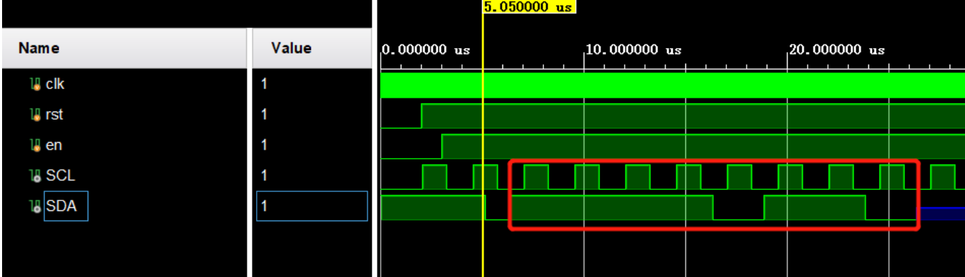
In the figure, when enable en is 1 and reset rst is on, transmission can be started. As can be seen from the yellow line in the figure, when SCL is high, SDA changes from high to low, and transmission starts.
Next, transmit the chip address and SDA output. It can be seen from the red box in the figure, 11110110
, it is our sending address (chip address seven bits + 0). Then there is the input state of SDA. At this time, it is high resistance. Manually input 0 as an answer signal.
2. Register 1 address and register 1 data:
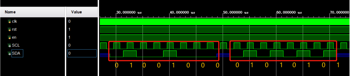
Connect to the above figure. After the chip address transmission is completed, the address of register 1 is transmitted. At red box 1 in the figure, it is 01001000, i.e. 0x48, and then the high resistance response
, continue to transmit the data of register 1. At red box 2 in the figure, it is 01010101, i.e. 0x55, and then respond with high resistance
. It can be seen that, like the data designed before, the simulation design is successful.
3. Register 2 address and register 2 data:
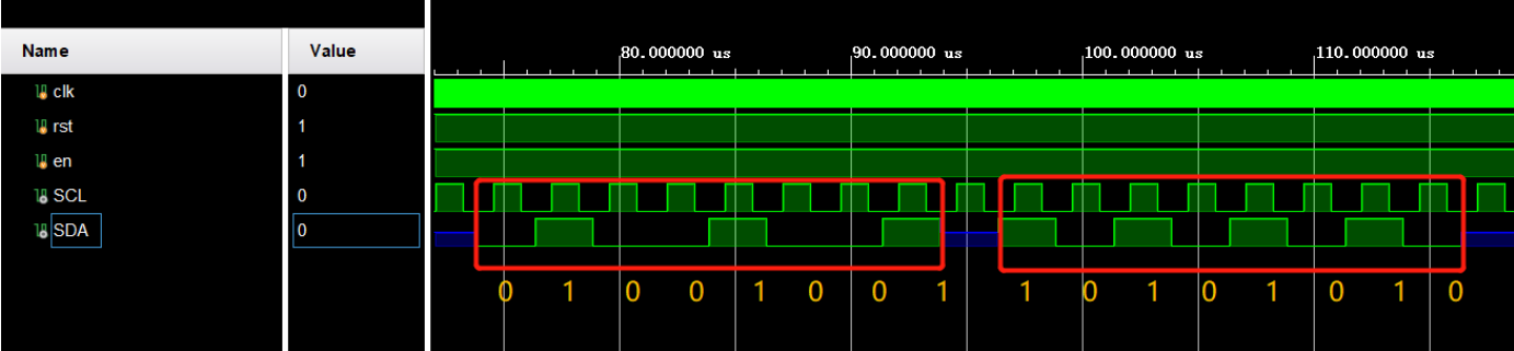
Connected to the above figure, similarly, the address and data of transmission register 2: address 01001001, i.e
0x49
, data 10101010, i.e. 0xAA
. Consistent with the design.
4. Register 3 address, register 3 data and termination status:
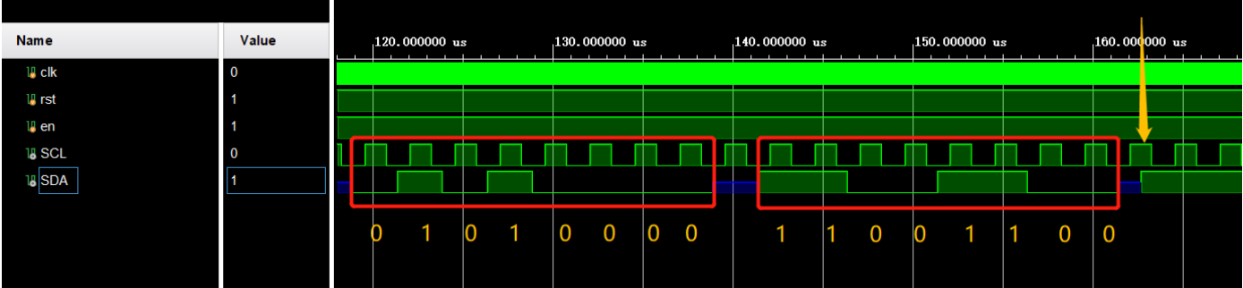
Connected to the above figure, similarly, the address and data of transmission register 3: address 01010000, i.e
0x50
, data 11001100, i.e. 0xCC
. Consistent with the design. Then when the next SCL is high,
SDA restore high power
Ping, terminate the transmission.
After the simulation, the result is consistent with the expectation and the simulation is successful. The following is testbench:
`timescale 1ns / 1ps
module IIC_control_tb( );
reg clk,rst,en;
wire SCL,SDA;
always #50 clk=~clk; // Generate 10MHz clock
initial begin
 rst<=0;
 clk<=0;
 en<=0;
 #2000 rst<=1;
 #1000 en<=1;

end
IIC_control iic(
 .clk(clk),
 .rst(rst),
 .SCL(SCL),
 .SDA(SDA),
 .en(en)
);
endmodule